

Motorola MGSF1N02ELT3, MGSF1N02ELT1 Datasheet
SEMICONDUCTOR TECHNICAL DATA
$ !
"
Order this document
by MGSF1N02ELT1/D
Motorola Preferred Device
# !""# !
Part of the GreenLine Portfolio of devices with energy–
conserving traits.
These miniature surface mount MOSFETs utilize Motorola’s
High Cell Density, HDTMOS process. Low r
minimal power loss and conserves energy, making this device
ideal for use in space sensitive power management circuitry.
Typical applications are dc–dc converters and power management in portable and battery–powered products such as
computers, printers, PCMCIA cards, cellular and cordless
telephones.
• Low r
Life
• Miniature SOT–23 Surface Mount Package Saves Board Space
MAXIMUM RATINGS
Drain–to–Source Voltage V
Gate–to–Source Voltage — Continuous V
Drain Current — Continuous @ TA = 25°C
Drain Current — Pulsed Drain Current (tp ≤ 10 µs)
Total Power Dissipation @ TA = 25°C P
Operating and Storage Temperature Range TJ, T
Thermal Resistance — Junction–to–Ambient R
Maximum Lead Temperature for Soldering Purposes, 1/8″ from case for 10 seconds T
Provides Higher Efficiency and Extends Battery
DS(on)
(TJ = 25°C unless otherwise noted)
Rating Symbol Value Unit
DS(on)
assures
1
GATE
3 DRAIN
2 SOURCE
N–CHANNEL
LOGIC LEVEL
ENHANCEMENT–MODE
TMOS MOSFET
3
1
2
CASE 318–08, Style 21
SOT–23 (TO–236AB)
DSS
GS
I
D
I
DM
θJA
D
stg
L
20 Vdc
± 8.0 Vdc
750
2000
400 mW
– 55 to 150 °C
300 °C/W
260 °C
mA
ORDERING INFORMATION
Device Reel Size Tape Width Quantity
MGSF1N02EL T1 7″ 8mm embossed tape 3000
MGSF1N02EL T3 13″ 8mm embossed tape 10,000
GreenLine is a trademark of Motorola, Inc.
HDTMOS is a trademark of Motorola, Inc. TMOS is a registered trademark of Motorola, Inc.
Thermal Clad is a trademark of the Bergquist Company.
Preferred devices are Motorola recommended choices for future use and best overall value.
Motorola Small–Signal Transistors, FETs and Diodes Device Data
Motorola, Inc. 1998
1
MGSF1N02ELT1
(
DD
,
D
,
ELECTRICAL CHARACTERISTICS
Characteristic Symbol Min Typ Max Unit
OFF CHARACTERISTICS
Drain–to–Source Breakdown Voltage
(VGS = 0 Vdc, ID = 10 µA)
Zero Gate Voltage Drain Current
(VDS = 20 Vdc, VGS = 0 Vdc)
(VDS = 20 Vdc, VGS = 0 Vdc, TJ = 125°C)
Gate–Source Leakage Current (VGS = ± 8.0 Vdc, VDS = 0 Vdc) I
ON CHARACTERISTICS
Gate–Source Threshold Voltage
(VDS = VGS, ID = 250 µAdc)
Static Drain–to–Source On–Resistance
(VGS = 4.5 Vdc, ID = 1.0 A)
(VGS = 2.5 Vdc, ID = 0.75 A)
DYNAMIC CHARACTERISTICS
Input Capacitance (VDS = 5.0 Vdc, VGS = 0 V, f = 1.0 Mhz) C
Output Capacitance (VDS = 5.0 Vdc, VGS = 0 V, f = 1.0 Mhz) C
Transfer Capacitance (VDG = 5.0 Vdc, VGS = 0 V, f = 1.0 Mhz) C
SWITCHING CHARACTERISTICS
Turn–On Delay Time
Rise Time
Turn–Off Delay Time
Fall Time t
Total Gate Charge (VDS = 16 Vdc, ID = 1.2 Adc,
SOURCE–DRAIN DIODE CHARACTERISTICS
Continuous Current I
Pulsed Current I
Forward Voltage
(1) Pulse Test: Pulse Width ≤ 300 µs, Duty Cycle ≤ 2%.
(2) Switching characteristics are independent of operating junction temperature.
(1)
(2)
(VGS = 0 Vdc, IS = 0.6 Adc) V
(TA = 25°C unless otherwise noted)
(2)
(VDD = 5 Vdc, ID = 1.0 Adc,
RL = 5 Ω, RG = 6 Ω)
VGS = 4.0 Vdc)
V
(BR)DSS
I
DSS
GSS
V
GS(th)
r
DS(on)
iss
oss
rss
t
d(on)
t
r
t
d(off)
f
Q
S
SM
SD
20 — — Vdc
—
—
— — ±0.1 µAdc
0.5 — 1.0 Vdc
—
—
— 160 — pF
— 130 —
— 60 —
— 6.0 —
— 26 —
— 117 —
— 105 —
T
— 6500 — pC
— — 0.6 A
— — 0.75
— — 1.2 V
—
—
—
—
1.0
10
0.085
0.115
µAdc
Ohms
ns
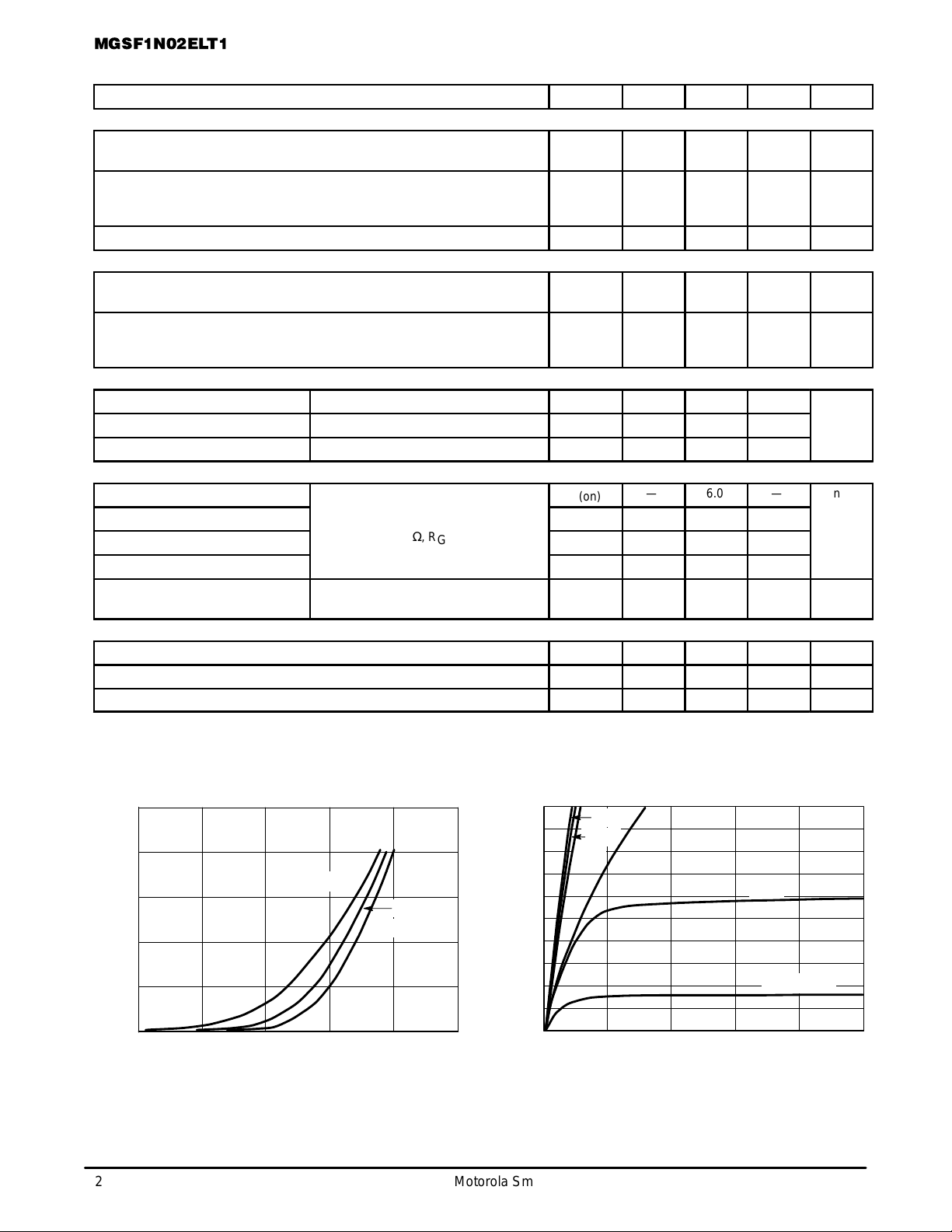
TYPICAL ELECTRICAL CHARACTERISTICS
2.5
2
TJ = 150°C
1.5
1
, DRAIN CURRENT (AMPS)
D
I
0.5
0
0.5 1.4 1.7
0.8 1.1
VGS, GATE–T O–SOURCE VOLTAGE (VOLTS)
25°C
–55°C
2.0
Figure 1. Transfer Characteristics
2
Motorola Small–Signal Transistors, FETs and Diodes Device Data
2
1.8
1.6
1.4
1.2
1
0.8
0.6
, DRAIN CURRENT (AMPS)
D
I
0.4
0.2
0
0 0.5 1 2.5
2.5 V
2.25 V
1.75 V
2.0 V
1.5 V
VGS = 1.25 V
1.5
VDS, DRAIN–TO–SOURCE VOL TAGE (VOLTS)
Figure 2. On–Region Characteristics
2
 Loading...