

Motorola MCM69Q618TQ6, MCM69Q618TQ6R, MCM69Q618TQ8, MCM69Q618TQ10, MCM69Q618TQ10R Datasheet
MOTOROLA
SEMICONDUCTOR TECHNICAL DATA
Advance Information
64K x 18 Bit Synchronous
Separate I/O Fast SRAM
The Motorola MCM69Q618 is a 1 Megabit static random access memory , organized
as 64K words of 18 bits. It features separate data input and data output buffers and
incorporates input and output registers on board with high speed SRAM.
The MCM69Q618 allows the user to perform transparent write and data pass
through. Two data bus ports are provided – a data input (D) and a data output (Q) port.
The synchronous design allows for precise cycle control with the use of an external
single clock (K). Address port, data input (D0 – D17), data output (Q0 – Q17), write enable (W
rising edge of clock (K).
writes can be intermixed. Thus, one can perform a read, a write, or a combination read/
write during any one cycle. For a combination read/write, the contents of the array are
read before the new data is written.
the contents of the array or the data presented to the input port D. For read/write or a
read cycle with G
is asserted, the Q port will instead output the data presented at the D input port.
• Single 3.3 V ± 5% Power Supply
• Fast Access Times: 6/8/10 ns Max
• Sustained Throughput of 1.49 Gigabits/Second
• Single Clock Operation
• Address, Data Input, E1
• 83 MHz Maximum Clock Cycle Time
• Self Timed Write
• Separate Data Input and Data Output Pins
• Pass–Through Feature
• Asynchronous Output Enable (G
• L VTTL Compatible I/O
• No Dead Cycles Required for Reads after Writes or for Writes after Reads
• 100 Pin TQFP Package
• Simultaneous Reads and Writes
Suggested Applications
), chip enables (E1, E2), and pass–through enable (PT) are registered on the
Any given cycle operates on only one address. However, for any cycle, reads and
By using the pass–through function, the output port Q can be made to reflect either
low, the Q port will output the contents of the array. However, if PT
, E2, PT, W, and Data Output Registers on Chip
)
— A TM — Ethernet Switches — Routers
— Cell/Frame Buffers — SNA Switches — Shared Memory
Order this document
by MCM69Q618/D
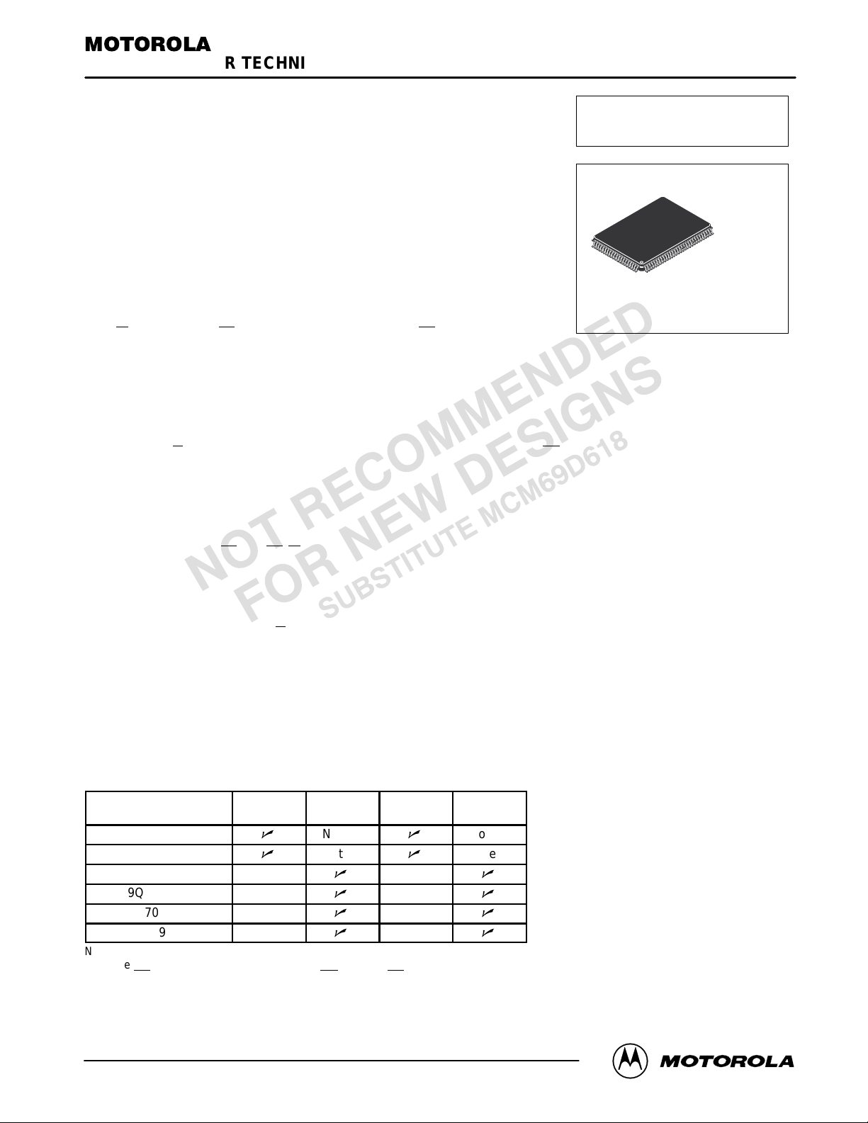
MCM69Q618
TQ PACKAGE
100 PIN TQFP
CASE 983A–01
Product Family Configurations
Part
Number
MCM69D536
MCM69D618
MCM69Q536
MCM69Q618
MCM67Q709
MCM67Q909
NOTES:
1. Tie AX and AY address ports together for the part to function as a single address part.
2. Tie GX
This document contains information on a new product. Specifications and information herein are subject to change without notice.
REV 5
11/24/97
Motorola, Inc. 1997
MOTOROLA FAST SRAM
high for DQX to be inputs and tie WY high and GY low for DQY to be outputs.
Dual
Address
n
n
Single
Address
Note 1
Note 1
n n
n n
n n
n n
Dual
I/O
n
n
Separate
I/O
Note 2
Note 2
MCM69Q618
1
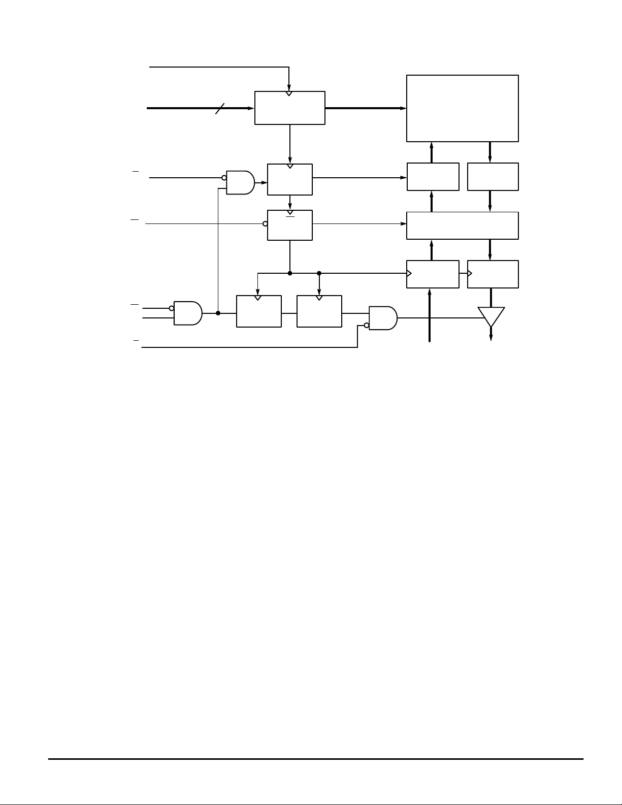
BLOCK DIAGRAM
K
A0 – A15
W
PT
E1
E2
G
16
ADDRESS
REGISTER
REGISTER
REGISTER
ENABLE
REGISTER 1
WRITE
PT
ENABLE
REGISTER 2
64K x 18 ARRAY
WRITE
DRIVER
PASS–THROUGH
DATA INPUT
REGISTER
D0 – D17 Q0 – Q17
SENSE
AMP
DATA OUTPUT
REGISTER
MCM69Q618
2
MOTOROLA FAST SRAM
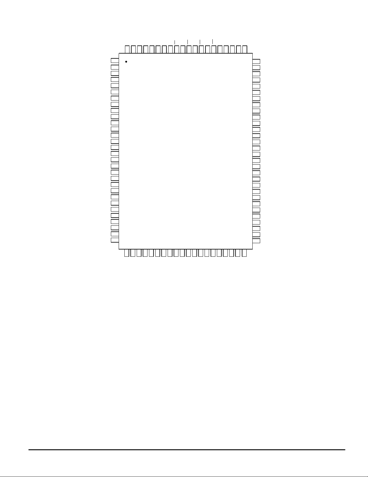
PIN ASSIGNMENT
V
DD
V
SS
D9
Q9
D10
Q10
V
DD
V
SS
D11
Q11
D12
Q12
V
DD
V
SS
Q13
D13
Q14
D14
V
DD
V
SS
Q15
D15
Q16
D16
V
DD
V
SS
Q17
D17
NC
A5
1
2
3
4
5
6
7
8
9
10
11
12
13
14
15
16
17
18
19
20
21
22
23
24
25
26
27
28
29
30
31 32 33
A6NCA7
DD
NC
VSSV
K
NC
94 9397 96 95 89 8892 91 90 86 8587100 99 98 81828384
37 3834 35 36 42 4339 40 41 45 4644
E1
G
E2
NC
PT
A8
NC
A9
NC
50494847
80
79
78
77
76
75
74
73
72
71
70
69
68
67
66
65
64
63
62
61
60
59
58
57
56
55
54
53
52
51
A15
NC
V
V
D8
Q8
D7
Q7
V
V
D6
Q6
D5
Q5
V
V
Q4
D4
Q3
D3
V
V
Q2
D2
Q1
D1
V
V
Q0
D0
NC
SS
DD
SS
DD
SS
DD
SS
DD
SS
DD
NC
W
A4NCA3
NC
NC
A2
NC
A1
NC
A0
V
DD
A10
NC
A11
NC
A12NCA13
NC
A14
MOTOROLA FAST SRAM
MCM69Q618
3
PIN DESCRIPTIONS
Pin Locations Symbol Type Description
30, 32, 34, 36, 38, 40, 42, 44, 46, 48, 50,
81, 83, 85, 98, 100
3, 5, 9, 11, 16, 18, 22, 24, 28, 52, 56, 58,
62, 64, 69, 71, 75, 77
90 E1 Input Synchronous Chip Enable: Active low for depth expansion.
91 E2 Input Synchronous Chip Enable: Active high for depth expansion.
92 G Input Asynchronous Output Enable Input:
96 K Input Clock: This signal registers the address, data in, and all control signals
86 PT Input Pass–through enable: Synchronous.
4, 6, 10, 12, 15, 17, 21, 23, 27, 53, 57,
59, 63, 65, 68, 70, 74, 76
88 W Input Synchronous Write.
1, 7, 13, 19, 25, 41, 54, 60, 66, 72, 78, 95 V
2, 8, 14, 20, 26, 55, 61, 67, 73, 79, 94 V
29, 31, 33, 35, 37, 39, 43, 45, 47, 49, 51,
80, 82, 84, 87, 89, 93, 97, 99
A0 – A15 Input Synchronous Address Inputs: These inputs are registered and must
D0 – D17 Input Synchronous Data Input.
Q0 – Q17 Output Synchronous Data Output.
DD
SS
NC — No Connection: There is no connection to the chip.
Supply + 3.3 V Power Supply.
Supply Ground.
meet setup and hold times.
Low — enables output buffers (Qx pins).
High — Qx pins are high impedance.
except G
.
TRUTH TABLE
Input at tn Clock Result from tn + 1 Clock Notes
Operation
Write and Pass–Through L H L L D written to A D data appears 1
Write/Read L H L H D written to A Q out from A 2
Pass–Through L H H L D data D data appears 3
Read L H H H Don’t Care Q out from A 4
Deselected X L X X Don’t Care Q is high–Z 5
Deselected H X X X Don’t Care Q is high–Z 6
NOTES:
1. W rite D to array and output D at Q.
2. Output contents of array to Q then write D to array.
3. Output D at Q. Do not write.
4. Output contents of array to Q. Do not write.
5. No operation.
6. No operation.
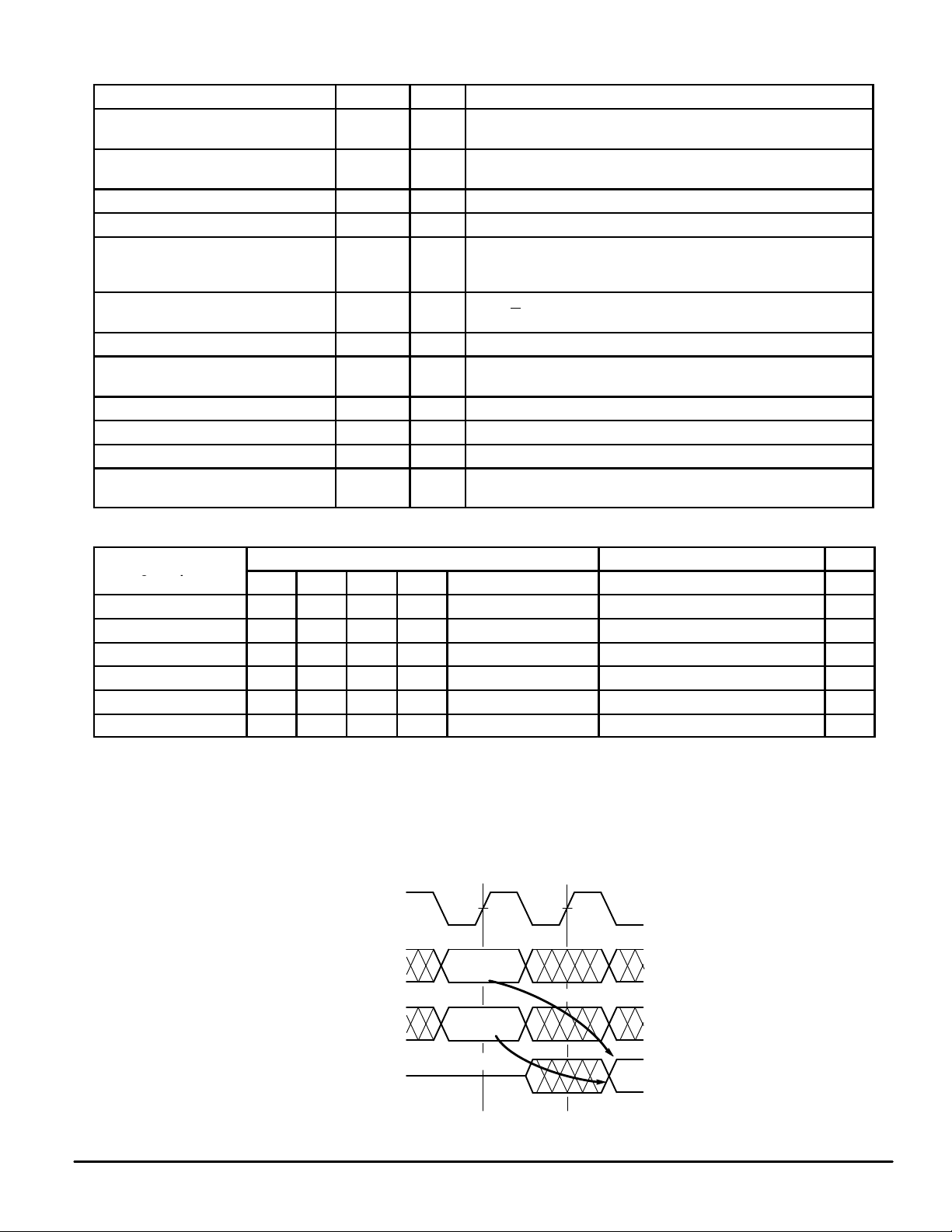
E1 E2 W PT Data Input D Data Output Q
K
ADDRESS & CONTROL
t
n
VALID
tn +
1
MCM69Q618
4
DATA INPUT D
DATA OUTPUT Q
PIPELINED READ ACCESS
VALID
PASS–THROUGH
VALID
MOTOROLA FAST SRAM
 Loading...