

Motorola MCM69P737TQ4R, MCM69P737TQ3.8R, MCM69P737TQ3.5R, MCM69P737TQ3.5, MCM69P737ZP3.5 Datasheet
...
MOTOROLA
SEMICONDUCTOR TECHNICAL DATA
128K x 36 Bit Pipelined
Bu rs t R AM Synchronous
Fast Static RAM
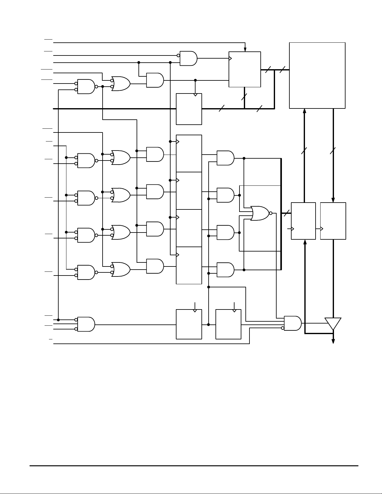
The MCM69P737 is a 4M bit synchronous fast static RAM designed to provide
a burstable, high performance, secondary cache for the PowerPC and other
high performance microprocessors. It is organized as 128K words of 36 bits
each. This device integrates input registers, an output register, a 2–bit address
counter, and high speed SRAM onto a single monolithic circuit for reduced parts
count in cache data RAM applications. Synchronous design allows precise cycle
control with the use of an external clock (K).
Addresses (SA), data inputs (DQx), and all control signals except output
enable (G
edge–triggered noninverting registers.
addresses can be generated internally by the MCM69P737 (burst sequence
operates in linear or interleaved mode dependent upon the state of LBO
controlled by the burst address advance (ADV
clock (K) input. This feature eliminates complex off–chip write pulse generation
and provides increased timing flexibility for incoming signals.
nous write enable (SW
to all bytes. The four bytes are designated as “a”, “b”, “c”, and “d”. SBa controls
DQa, SBb
writes SBx
or if all SBx
edge–triggered output register and then released to the output buffers at the next
rising edge of clock (K).
operate on a 2.5 V or 3.3 V power supply . All inputs and outputs are JEDEC standard JESD8–5 compatible.
• MCM69P737–3.5: 3.5 ns Access/6 ns Cycle (166 MHz)
• 3.3 V + 10%, – 5% Core Power Supply , 2.5 V or 3.3 V I/O Supply
• ADSP
• Selectable Burst Sequencing Order (Linear/Interleaved)
• Single–Cycle Deselect Timing
• Internally Self–Timed Write Cycle
• Byte Write and Global Write Control
• PB1 Version 2.0 Compatible
• JEDEC Standard 119–Pin PBGA and 100–Pin TQFP Packages
) and linear burst order (LBO) are clock (K) controlled through positive–
Bursts can be initiated with either ADSP
Write cycles are internally self–timed and are initiated by the rising edge of the
Synchronous byte write (SBx
) are provided to allow writes to either individual bytes or
controls DQb, etc. Individual bytes are written if the selected byte
are asserted with SW. All bytes are written if either SGW is asserted
and SW are asserted.
For read cycles, pipelined SRAMs output data is temporarily stored by an
The MCM69P737 operates from a 3.3 V core power supply and all outputs
MCM69P737–3.8: 3.8 ns Access/6.7 ns Cycle (150 MHz)
MCM69P737–4: 4 ns Access/7.5 ns Cycle (133 MHz)
, ADSC, and ADV Burst Control Pins
), synchronous global write (SGW), and synchro-
or ADSC input pins. Subsequent burst
) and
) input pin.
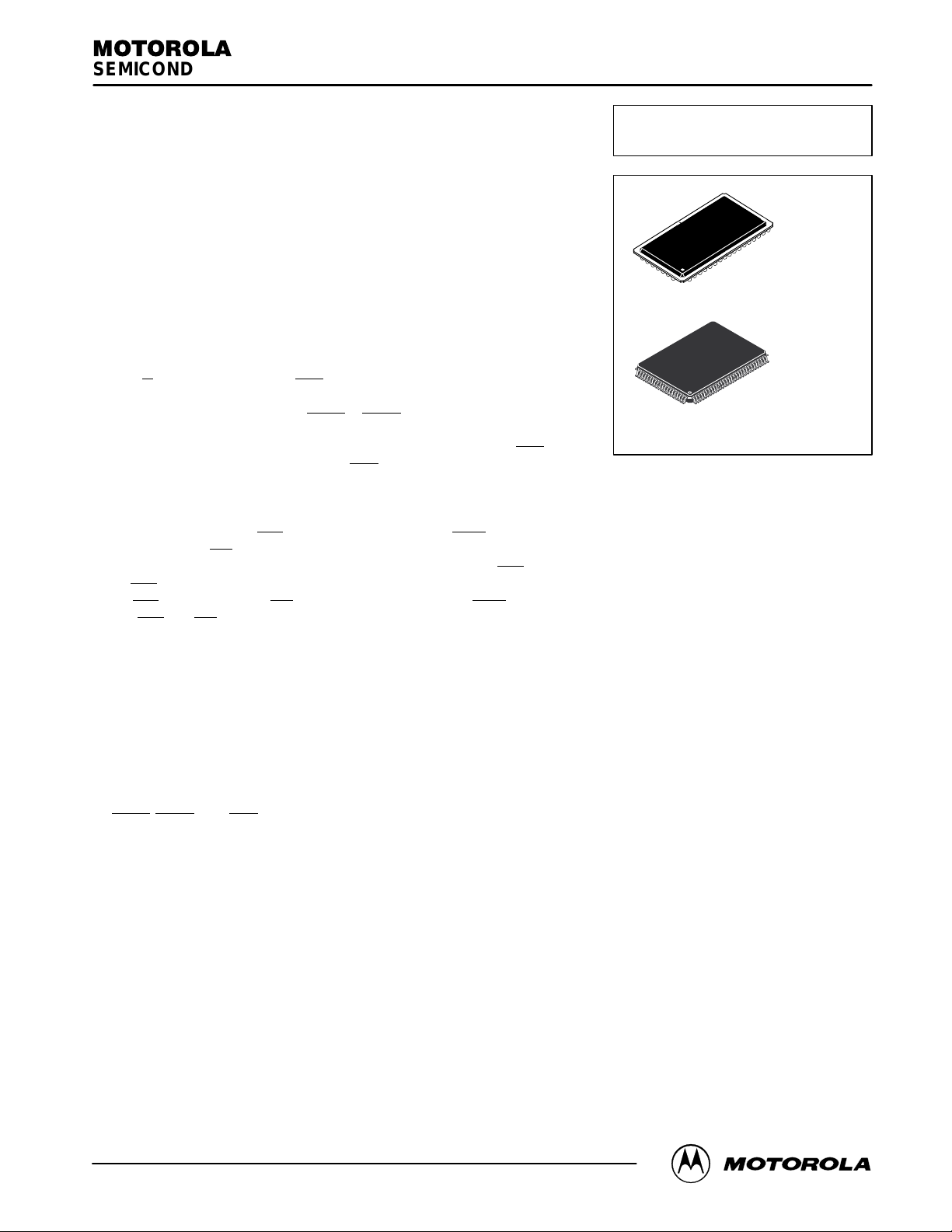
Order this document
by MCM69P737/D
MCM69P737
ZP PACKAGE
PBGA
CASE 999–02
TQ PACKAGE
TQFP
CASE 983A–01
The PowerPC name is a trademark of IBM Corp., used under license therefrom.
REV 6
1/20/98
Motorola, Inc. 1998
MOTOROLA FAST SRAM
MCM69P737
1
LBO
ADV
K
ADSC
ADSP
SA
SA1
SA0
SGW
FUNCTIONAL BLOCK DIAGRAM
K2
ADDRESS
REGISTER
17
BURST
COUNTER
CLR
2
15
2
17
128K x 36
ARRAY
SW
SBa
SBb
SBc
SBd
SE1
SE2
SE3
WRITE
REGISTER
a
WRITE
REGISTER
b
WRITE
REGISTER
c
WRITE
REGISTER
d
K2 K
ENABLE
REGISTER
ENABLE
REGISTER
4
DATA–IN
REGISTER
K
36
36
DATA–OUT
REGISTER
G
MCM69P737
2
DQa – DQd
MOTOROLA FAST SRAM
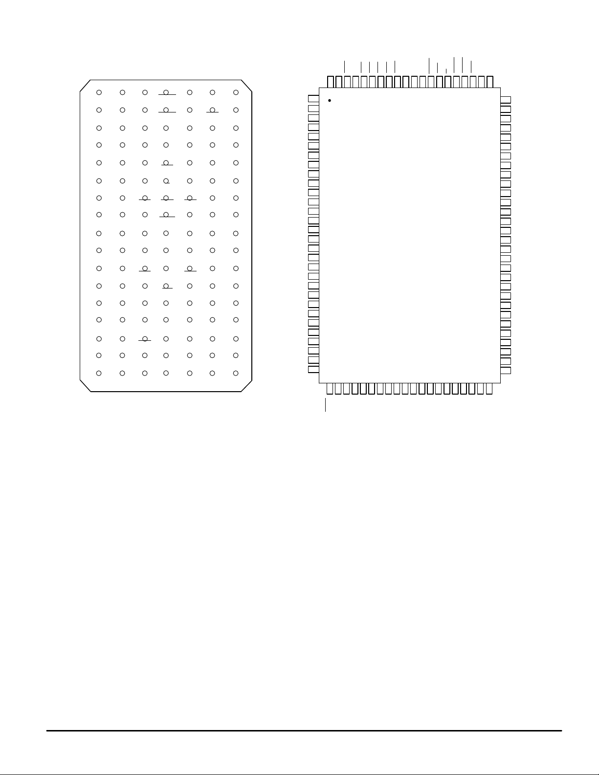
PIN ASSIGNMENTS
6543217
A
V
SA SA SA SA
DDQ
B
NC SE2 SA ADSC
C
D
E
F
G
H
J
K
L
M
N
P
R
T
U
SA SA SA SA
NC
DQc DQc VSSNC DQb
DQcDQc
V
DQc V
DDQ
DQc
DQc VSSSGW
V
V
V
DD
DDQ
DQd DQd V
DQd V
DDQ
DQdDQd
DQd DQd VSSSA0
SA SA
NC
NC SA SA NC
NC
DDQ
SS
SS
SBcDQcDQc
NCV
SS
SBdDQdDQd
SS
SS
LBO
NCNC
ADSP
SA
V
DD
V
SS
V
SS
V
G
SS
SBb
V
SS
NCV
DD
KV
SS
NC
SW
V
SS
V
SS
V
SS
NCV
DD
SA
NC
NC
SE3
DQbSE1V
DQb
DQbADV
DQb
V
DD
DQa
DQaSBa
DQa
DQaSA1V
DQa
NC
V
V
V
V
V
DDQ
NC
NC
DQb
DQb
DDQ
DQb
DQb
DDQ
DQa
DQa
DDQ
DQa
DQa
NC
NC
DDQ
V
V
V
V
DQc
DQc
DQc
DDQ
V
SS
DQc
DQc
DQc
DQc
V
SS
DDQ
DQc
DQc
NC
V
DD
NC
V
SS
DQd
DQd
DDQ
V
SS
DQd
DQd
DQd
DQd
V
SS
DDQ
DQd
DQd
DQd
1
2
3
4
5
6
7
8
9
10
11
12
13
14
15
16
17
18
19
20
21
22
23
24
25
26
27
28
29
30
31 3233
SASASE1
DD
SE2
SBc
SBa
SBb
SBd
94 93979695 89889291 90 86858710099 98 81828384
3738343536 42433940 41 454644
SE3
K
VSSV
SW
SGW
G
ADSP
ADSC
ADV
SA
50494847
80
79
78
77
76
75
74
73
72
71
70
69
68
67
66
65
64
63
62
61
60
59
58
57
56
55
54
53
52
51
SA
DQb
DQb
DQb
V
DDQ
V
SS
DQb
DQb
DQb
DQb
V
SS
V
DDQ
DQb
DQb
V
SS
NC
V
DD
NC
DQa
DQa
V
DDQ
V
SS
DQa
DQa
DQa
DQa
V
SS
V
DDQ
DQa
DQa
DQa
TOP VIEW 119 BUMP PBGA
SASASA
LBO
SA
SA1
TOP VIEW 100 PIN TQFP
SA0
NC
NC
V
SS
DD
V
NC
NC
SA
SASASA
SA
SA
SA
Not to Scale
MOTOROLA FAST SRAM
MCM69P737
3
PBGA PIN DESCRIPTIONS
Pin Locations Symbol Type Description
4B ADSC Input Synchronous Address Status Controller: Active low, interrupts any
4A ADSP Input Synchronous Address Status Processor: Active low, interrupts any
4G ADV Input Synchronous Address Advance: Increments address count in
(a) 6K, 7K, 6L, 7L, 6M, 6N, 7N, 6P, 7P
(b) 6D, 7D, 6E, 7E, 6F, 6G, 7G, 6H, 7H
(c) 1D, 2D, 1E, 2E, 2F, 1G, 2G, 1H, 2H
(d) 1K, 2K, 1L, 2L, 2M, 1N, 2N, 1P, 2P
4F G Input Asynchronous Output Enable Input:
4K K Input Clock: This signal registers the address, data in, and all control signals
3R LBO Input Linear Burst Order Input: This pin must remain in steady state (this
2A, 3A, 5A, 6A, 3B, 5B, 2C, 3C,
5C, 6C, 2R, 6R, 3T, 4T, 5T
4N, 4P SA1, SA0 Input Synchronous Address Inputs: These pins must be wired to the two
5L, 5G, 3G, 3L
(a) (b) (c) (d)
4E SE1 Input Synchronous Chip Enable: Active low to enable chip.
2B SE2 Input Synchronous Chip Enable: Active high for depth expansion.
6B SE3 Input Synchronous Chip Enable: Active low for depth expansion.
4H SGW Input Synchronous Global Write: This signal writes all bytes regardless of the
4M SW Input Synchronous Write: This signal writes only those bytes that have been
4C, 2J, 4J, 6J, 4R V
1A, 7A, 1F, 7F, 1J, 7J, 1M, 7M, 1U, 7U V
3D, 5D, 3E, 5E, 3F, 5F, 3H, 5H,
3K, 5K, 3M, 5M, 3N, 5N, 3P, 5P
1B, 7B, 1C, 7C, 4D, 3J, 5J, 4L, 1R, 5R,
7R, 1T, 2T, 6T, 7T, 2U, 3U, 4U, 5U, 6U
ongoing burst and latches a new external address. Used to initiate a
READ, WRITE, or chip deselect.
ongoing burst and latches a new external address. Used to initiate a
new READ, WRITE, or chip deselect (exception — chip deselect does
not occur when ADSP
accordance with counter type selected (linear/interleaved).
DQx I/O Synchronous Data I/O: “x” refers to the byte being read or written
SA Input Synchronous Address Inputs: These inputs are registered and must
SBx Input Synchronous Byte Write Inputs: “x” refers to the byte being written (byte
DD
DDQ
V
SS
NC — No Connection: There is no connection to the chip.
Supply Core Power Supply.
Supply I/O Power Supply.
Supply Ground.
(byte a, b, c, d).
Low — enables output buffers (DQx pins).
High — DQx pins are high impedance.
except G
signal not registered or latched). It must be tied high or low.
Low — linear burst counter (68K/PowerPC).
High — interleaved burst counter (486/i960/Pentium).
meet setup and hold times.
LSBs of the address bus for proper burst operation. These inputs are
registered and must meet setup and hold times.
a, b, c, d). SGW
Negated high — blocks ADSP
asserted.
status of the SBx
being used, tie this pin high.
selected using the byte write SBx
are being used, tie this pin low.
and LBO.
is asserted and SE1 is high).
overrides SBx.
or deselects chip when ADSC is
and SW signals. If only byte write signals SBx are
pins. If only byte write signals SBx
MCM69P737
4
MOTOROLA FAST SRAM
TQFP PIN DESCRIPTIONS
Pin Locations Symbol
85 ADSC Input Synchronous Address Status Controller: Active low, interrupts any
84 ADSP Input Synchronous Address Status Processor: Active low, interrupts any
83 ADV Input Synchronous Address Advance: Increments address count in
(a) 51, 52, 53, 56, 57, 58, 59, 62, 63
(b) 68, 69, 72, 73, 74, 75, 78, 79, 80
(c) 1, 2, 3, 6, 7, 8, 9, 12, 13
(d) 18, 19, 22, 23, 24, 25, 28, 29, 30
86 G Input Asynchronous Output Enable Input:
89 K Input Clock: This signal registers the address, data in, and all control signals
31 LBO Input Linear Burst Order Input: This pin must remain in steady state (this
32, 33, 34, 35, 44, 45, 46,
47, 48, 49, 50, 81, 82, 99, 100
36, 37 SA1, SA0 Input Synchronous Address Inputs: these pins must be wired to the two LSBs
93, 94, 95, 96
(a) (b) (c) (d)
98 SE1 Input Synchronous Chip Enable: Active low to enable chip.
97 SE2 Input Synchronous Chip Enable: Active high for depth expansion.
92 SE3 Input Synchronous Chip Enable: Active low for depth expansion.
88 SGW Input Synchronous Global Write: This signal writes all bytes regardless of the
87 SW Input Synchronous Write: This signal writes only those bytes that have been
15, 41, 65, 91 V
4, 11, 20, 27, 54, 61, 70, 77 V
5, 10, 17, 21, 26, 40,
55, 60, 67, 71, 76, 90
14, 16, 38, 39, 42, 43, 64, 66 NC — No Connection: There is no connection to the chip.
DQx I/O Synchronous Data I/O: “x” refers to the byte being read or written
SA Input Synchronous Address Inputs: These inputs are registered and must
SBx Input Synchronous Byte Write Inputs: “x” refers to the byte being written (byte
DD
DDQ
V
SS
Type Description
ongoing burst and latches a new external address. Used to initiate a
READ, WRITE, or chip deselect.
ongoing burst and latches a new external address. Used to initiate a
new READ, WRITE, or chip deselect (exception — chip deselect does
not occur when ADSP
accordance with counter type selected (linear/interleaved).
(byte a, b, c, d).
Low — enables output buffers (DQx pins).
High — DQx pins are high impedance.
except G
signal not registered or latched). It must be tied high or low.
Low — linear burst counter (68K/PowerPC).
High — interleaved burst counter (486/i960/Pentium).
meet setup and hold times.
of the address bus for proper burst operation. These inputs are
registered and must meet setup and hold times.
a, b, c, d). SGW
Negated high — blocks ADSP
asserted.
status of the SBx
being used, tie this pin high.
selected using the byte write SBx
are being used, tie this pin low.
Supply Core Power Supply.
Supply I/O Power Supply.
Supply Ground.
and LBO.
is asserted and SE1 is high).
overrides SBx.
or deselects chip when ADSC is
and SW signals. If only byte write signals SBx are
pins. If only byte write signals SBx
MOTOROLA FAST SRAM
MCM69P737
5
TRUTH TABLE (See Notes 1 Through 5)
Address
Next Cycle
Deselect None 1 X X X 0 X X High–Z X
Deselect None 0 X 1 0 X X X High–Z X
Deselect None 0 0 X 0 X X X High–Z X
Deselect None X X 1 1 0 X X High–Z X
Deselect None X 0 X 1 0 X X High–Z X
Begin Read External 0 1 0 0 X X X High–Z X
Begin Read External 0 1 0 1 0 X X High–Z READ
Continue Read Next X X X 1 1 0 1 High–Z READ
Continue Read Next X X X 1 1 0 0 DQ READ
Continue Read Next 1 X X X 1 0 1 High–Z READ
Continue Read Next 1 X X X 1 0 0 DQ READ
Suspend Read Current X X X 1 1 1 1 High–Z READ
Suspend Read Current X X X 1 1 1 0 DQ READ
Suspend Read Current 1 X X X 1 1 1 High–Z READ
Suspend Read Current 1 X X X 1 1 0 DQ READ
Begin Write External 0 1 0 1 0 X X High–Z WRITE
Continue Write Next X X X 1 1 0 X High–Z WRITE
Continue Write Next 1 X X X 1 0 X High–Z WRITE
Suspend Write Current X X X 1 1 1 X High–Z WRITE
Suspend Write Current 1 X X X 1 1 X High–Z WRITE
NOTES:
1. X = Don’t Care. 1 = logic high. 0 = logic low.
2. Write is defined as either 1) any SBx
3. G
is an asynchronous signal and is not sampled by the clock K. G drives the bus immediately (t
4. On write cycles that follow read cycles, G
also remain negated at the completion of the write cycle to ensure proper write data hold times.
5. This read assumes the RAM was previously deselected.
Used
SE1 SE2 SE3 ADSP ADSC ADV G
and SW low or 2) SGW is low.
must be negated prior to the start of the write cycle to ensure proper write data setup times. G must
3
DQx Write 2,
) following G going low.
GLQX
4
5
5
LINEAR BURST ADDRESS TABLE (LBO = V
1st Address (External) 2nd Address (Internal) 3rd Address (Internal) 4th Address (Internal)
X . . . X00 X . . . X01 X . . . X10 X . . . X11
X . . . X01 X . . . X10 X . . . X11 X . . . X00
X . . . X10 X . . . X11 X . . . X00 X . . . X01
X . . . X11 X . . . X00 X . . . X01 X . . . X10
INTERLEAVED BURST ADDRESS TABLE (LBO = V
1st Address (External) 2nd Address (Internal) 3rd Address (Internal) 4th Address (Internal)
X . . . X00 X . . . X01 X . . . X10 X . . . X11
X . . . X01 X . . . X00 X . . . X11 X . . . X10
X . . . X10 X . . . X11 X . . . X00 X . . . X01
X . . . X11 X . . . X10 X . . . X01 X . . . X00
SS
)
)
DD
WRITE TRUTH TABLE
Cycle Type SGW SW SBa SBb SBc SBd
Read H H X X X X
Read H L H H H H
Write Byte a H L L H H H
Write Byte b H L H L H H
Write Byte c H L H H L H
Write Byte d H L H H H L
Write All Bytes H L L L L L
Write All Bytes L X X X X X
MCM69P737
6
MOTOROLA FAST SRAM
 Loading...