

Motorola MCM69C232TQ20, MCM69C232TQ20R Datasheet
MOTOROLA
SEMICONDUCTOR TECHNICAL DATA
Advance Information
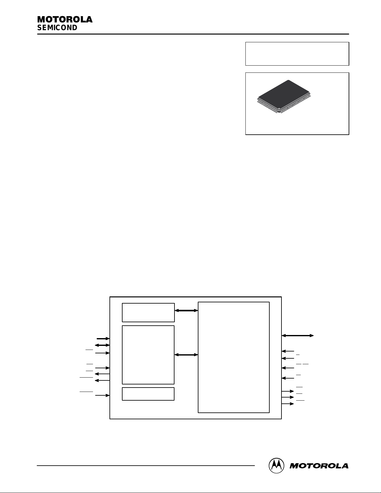
4K x 64 CAM
The MCM69C232 is a flexible content–addressable memory (CAM) that can
contain 4096 entries of 64 bits each. The widths of the match field and the output
field are programmable, and the match time is designed to be 160 ns. As a result,
the MCM69C232 is well suited for datacom applications such as Virtual Path
Identifier/Virtual Circuit Identifier (VPI/VCI) translation in ATM switches up to
OC12 (622 Mbps) data rates and Media Access Control (MAC) address lookup
in Ethernet/Fast Ethernet bridges. The match duty cycle of the MCM69C232 is
user defined, with a trade–off between the time between matches and the number of new entries added to the CAM per second.
• 4096 Entries
• 160 ns Match Time
• Mask Register to “Don’t Care” Selected Bits
• Depth Expansion by Cascading Multiple Devices
• 50 MHz Maximum Clock Rate
• Programmable Match and Output Field Widths
• Concurrent Matching of Virtual Path Circuits and Virtual Connection
Circuits in ATM Mode
• Separate Ports for Control and Match Operations
• 200 ns Insertion Time if One of Twelve Entry Queue Locations is Empty
• 12 ms Initialization Time After Fast Insertion (at Power–Up Only)
• Single 3.3 V ± 5% Supply
• 100 Pin TQFP Package
• IEEE Standard 1 149.1 Test Port (JTAG)
Order this document
by MCM69C232/D
MCM69C232
TQ PACKAGE
TQFP
CASE 983A–01
Related Products
— MCM69D536, MCM69D618 (Dual I/O, Dual Address RAMs)
— MCM67Q709A, MCM67Q909 (Separate I/O RAMs)
— MCM69C432 (CAM)
CONTROL PORT
12 x 64
ENTRY QUEUE
A2 – A0
DQ15 – DQ0
SEL
WE
IRQ
DTACK
RESET
This document contains information on a new product. Specifications and information herein are subject to change without notice.
STATUS/
CONTROL
LOGIC
INPUT REG
4K x 64
CAM
TABLE
MATCH PORT
MQ31 – MQ0
K
G
LH/SM
LL
MC
MS
VPC
REV 3
1/15/98
Motorola, Inc. 1998
MOTOROLA FAST SRAM
MCM69C232
1
PIN ASSIGNMENT
MQ9
MQ8
V
SS
V
DD
MQ7
MQ6
MQ5
MQ4
V
SS
V
DD
MQ3
MQ2
MQ1
MQ0
V
SS
V
DD
DQ15
DQ14
DQ13
DQ12
V
SS
V
DD
DQ11
DQ10
DQ9
DQ8
V
DD
V
SS
DQ7
DQ6
MQ10
1
2
3
4
5
6
7
8
9
10
11
12
13
14
15
16
17
18
19
20
21
22
23
24
25
26
27
28
29
30
31 32 33
DD
MQ11
VSSV
MQ14
MQ12
MQ15
MQ13
94 9397 96 95 89 8892 91 90 86 8587100 99 98 81828384
37 3834 35 36 42 4339 40 41 45 4644
LL
V
DD
V
SS
LH/SM
MQ16
MQ17
MQ19
MQ18
V
DD
V
SS
MQ20
MQ21
80
79
78
77
76
75
74
73
72
71
70
69
68
67
66
65
64
63
62
61
60
59
58
57
56
55
54
53
52
51
50494847
MQ22
MQ23
V
SS
V
DD
MQ24
MQ25
MQ26
MQ27
V
SS
V
DD
MQ28
MQ29
MQ30
MQ31
V
SS
V
DD
MC
VPC
MS
G
V
SS
V
DD
DTACK
IRQ
RESET
TDO
V
DD
V
SS
TCK
TMS
DQ5
DQ4
V
DD
SS
V
DQ3
DQ2
DQ1
DQ0
K
V
SS
V
DD
A2
A1
A0
WE
SEL
VDDV
DD
TDI
TRST
MCM69C232
2
MOTOROLA FAST SRAM
PIN DESCRIPTIONS
Pin Locations Symbol Type Description
42 – 44 A2 – A0 Input 3–bit control port address bus.
58 DTACK Output Control port data transfer acknowledge (Open Drain).
17 – 20, 23 – 26,
29 – 32, 35 – 38
61 G Input Asynchronous Output Enable control of MQ31 – MQ0.
57 IRQ Output Control port interrupt (Open Drain).
39 K Input Interface Clock, max frequency of 50 MHz.
89 LH/SM Input Latch High/Start Match. Initiates match sequence on match data present on
92 LL Input Latch Low. Latches low order bits if match width is > 32 bits.
64 MC Output Match Complete (Open Drain).
62 MS Output Match Successful (Open Drain).
67 – 70, 73 – 76,
79 – 82, 85 – 88,
93 – 96, 99, 100,
1, 2, 5 – 8, 11 – 14
56 RESET Input Resets chip to a known state.
46 SEL Input Control port chip select, active low.
52 TCK Input Test Clock, part of JTAG interface.
50 TDI Input Test Data In, part of JTAG interface.
55 TDO Output Test Data Out, part of JTAG interface.
51 TMS Input Test Mode Select, part of JTAG interface.
49 TRST Input TAP Reset part of JTAG interface.
63 VPC Output Virtual Path Circuit. Used in ATM mode to indicate a virtual path circuit match has
45 WE Input Control port Write Enable.
4, 10, 16, 22, 27, 33,
41, 47, 48, 54, 59, 65,
71, 77, 84, 91, 97
3, 9, 15, 21, 28, 34,
40, 53, 60, 66, 72,
78, 83, 90, 98
DQ15 – DQ0 I/O 16–bit bidirectional control port data bus.
MQ31 – MQ0.
MQ31 – MQ0 I/O 32–bit common I/O CAM data. Used for input of match RAM and data RAM
V
DD
V
SS
Supply Power Supply: 3.3 V ± 5%.
Supply Ground.
values.
occurred (Open Drain).
MOTOROLA FAST SRAM
MCM69C232
3
ABSOLUTE MAXIMUM RATINGS (See Note 1)
Rating Symbol Value Unit
Supply Voltage (see Note 2) V
Voltage Relative to VSS (see Note 2) V
Output Current per Pin I
Package Power Dissipation (see Note 3) P
Temperature Under Bias (see Note 3) T
Operating Temperature (see Note 4) T
Storage Temperature T
NOTES:
1. Permanent device damage may occur if ABSOLUTE MAXIMUM RATINGS are
exceeded. Functional operation should be restricted to RECOMMENDED OPERATING CONDITIONS. Exposure to higher than recommended voltages for extended
periods of time could affect device reliability.
2. All voltages are referenced to VSS.
3. Power dissipation capability will be dependent upon package characteristics and use
environment. See Package Thermal Characteristics.
4. Consult Junction to Ambient Thermal Characteristics table for details and conditions.
DD
in
out
D
bias
A
stg
– 0.5 to VDD + 0.5 V V
4.6 V
± 20 mA
— W
– 10 to 85 °C
0 to 70 °C
– 55 to 125 °C
DC OPERA TING CONDITIONS AND CHARACTERISTICS
(VDD = 3.3 V ± 5%, TJ = 20 to 120°C, Unless Otherwise Noted)
This device contains circuitry to protect the
inputs against damage due to high static voltages or electric fields; however, it is advised
that normal precautions be taken to avoid
application of any voltage higher than maximum rated voltages to this high–impedance
circuit.
RECOMMENDED OPERATING CONDITIONS
Parameter Symbol Min Typ Max Unit
Power Supply Voltage V
Operating Temperature (Junction) T
Input Low Voltage V
Input High Voltage V
*VIL (min) = – 3.0 V ac (pulse width v 20 ns).
(Voltages Referenced to VSS = 0 V)
DD
J
IL
IH
3.1 3.3 3.5 V
20 — 120 °C
– 0.5* 0 0.8 V
2.0 3 5.5 V
DC CHARACTERISTICS AND SUPPLY CURRENTS
Parameter Symbol Min Max Unit
Active Power Supply Current @ 20°C T
Active Power Supply Current @ 120°C T
Input Leakage Current (0 V v Vin v VDD) I
Output Leakage Current (0 V v Vin v VDD) I
Output Low Voltage (IOL = 8 mA) V
Output High Voltage (IOH = – 4 mA) V
J
J
I
DD1
I
DD2
(I) — TBD µA
lkg
(O) — TBD µA
lkg
OL
OH
— 575 mA
— 460 mA
— 0.4 V
2.4 — V
PACKAGE THERMAL CHARACTERISTICS
Rating Symbol Max Unit
Thermal Resistance Junction to Ambient (200 lfpm, 4 Layer Board) (Note 2) R
Thermal Resistance Junction to Board (Bottom) (Note 3) R
Thermal Resistance Junction to Case (Top) (Note 4) R
NOTES:
1. RAM junction temperature is a function of on–chip power dissipation, package thermal impedance, mounting site temperature, and
mounting site thermal impedance.
2. Per SEMI G38–87.
3. Indicates the average thermal impedance between the die and the mounting surface.
4. Indicates the average thermal impedance between the die and the case top surface. Measured via the cold plate method (MIL SPEC–883
Method 1012.1).
θJA
θJB
θJC
27.1 °C/W
17 °C/W
9 °C/W
MCM69C232
4
MOTOROLA FAST SRAM
CAPACITANCE (Periodically Sampled Rather Than 100% Tested)
Parameter Symbol Min Max Unit
Input Capacitance C
I/O Capacitance C
JUNCTION TO AMBIENT THERMAL CHARACTERISTICS
Board Air (LFPM) θJA (°C/W) Maximum Ambient Temperature (°C)
1 Layer 0 40.1 55.8
1 Layer 200 34.7 64.4
1 Layer 400 32.1 68.7
4 Layer 0 30.5 71.1
4 Layer 200 27.1 76.6
4 Layer 400 25.6 79.0
AC OPERA TING CONDITIONS AND CHARACTERISTICS
(VDD = 3.3 V ± 5%, TJ = 20 to 120°C, Unless Otherwise Noted)
I/O
in
— 5 pF
— 8 pF
Input Timing Measurement Reference Level 1.5 V. . . . . . . . . . . . . . .
Input Pulse Levels 0 to 3.0 V. . . . . . . . . . . . . . . . . . . . . . . . . . . . . . . . .
Input Rise/Fall Time 3 ns. . . . . . . . . . . . . . . . . . . . . . . . . . . . . . . . . . . .
Output Timing Reference Level 1.5 V. . . . . . . . . . . . . . . . . . . . . . . . . .
Output Load Figure 1 Unless Otherwise Noted. . . . . . . . . . . . . . . . . .
CONTROL PORT AND MATCH PORT TIMINGS
(Voltages Referenced to VSS = 0 V, Max’s are t
Parameter
CONTROL PORT TIMING
Address Valid to SEL Low t
DTACK Low to Address Invalid t
Data Valid to Select Low t
DTACK Low to Data Invalid t
Output Valid to DTACK Low t
WE Valid to Select Low t
DTACK Low to WE High t
WE High to Output Active t
Select Low to DTACK Low* t
Select High to DTACK High t
DTACK Low to IRQ Low t
IRQ Low to IRQ High t
DTACK Low to Select High t
DTACK High to Select Low t
Address Valid to Output Valid t
Select High to Output Three–State t
*DTACK is delayed when a write is attempted during certain operations. See Functional Description.
Dependent and Listed Values are for t
KHKH
KHKH
Symbol Min Max Unit
AVSL
DTLAX
DVSL
DTLDX
QVDTL
WVSL
DTLWH
WHQX
SLDTL
SHDTH
DTLIL
ILIH
DTLSH
DTHSL
AVQV
SHQZ
= 20 ns)
0 — ns
0 — ns
0 — ns
0 — ns
2 — ns
0 — ns
0 — ns
TBD — ns
10 — ns
10 30 ns
TBD — ns
20 — ns
0 — ns
0 — ns
— 8 ns
— 8 ns
MOTOROLA FAST SRAM
MCM69C232
5
CONTROL PORT AND MATCH PORT TIMINGS
(Voltages Referenced to VSS = 0 V, Max’s are t
Parameter
MATCH PORT TIMING
Clock Cycle Time t
Clock High Time t
Clock Low Time t
Clock High to LHSM or LL Low t
Clock High to LHSM or LL High t
MQ Input Data Setup Time to Clock High t
Clock High to Match Data Hold Time t
Clock High to MQ Valid t
Clock High to MC High t
Clock High to MC Low t
Clock High to MS Low t
Clock High to MS High t
Clock High to VPC Low t
Clock High to VPC High t
G Low to MQ Active t
G High to MQ High–Z t
LH/SM Low to LH/SM Low t
Dependent and Listed Values are for t
KHKH
= 20 ns)
KHKH
Symbol Min Max Unit
KHKH
KHKL
KLKH
KHLL
KHLH
MQVKH
KHMQX
KHMQV
KHMCH
KHMCL
KHMSL
KHMSH
KHVPL
KHVPH
GLMQX
GHMQZ
SMSM
20 250 ns
8 242 ns
8 242 ns
— 7 ns
— 7 ns
8 — ns
2 — ns
— 12 ns
— 5 ns
— 5 ns
— 12 ns
— 5 ns
— 12 ns
— 5 ns
3.8 — ns
— 4 ns
10 — cycles
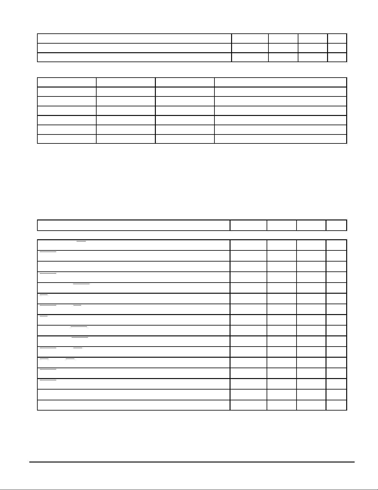
OUTPUT
Z0 = 50
RL = 50
Ω
VL = 1.5 V
Figure 1. AC Test Loads
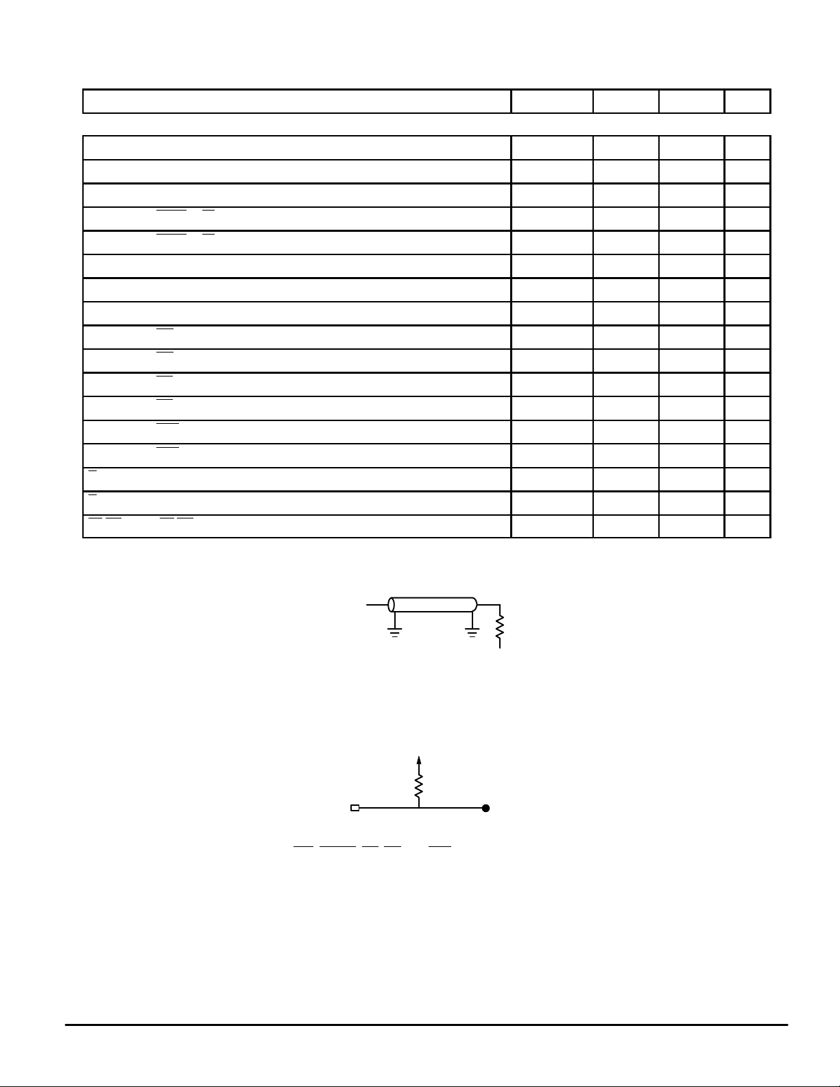
3.3 V
R
H
MCM69C232 OUTPUT PIN
NOTES:
1. For IRQ
2. If multiple MCM69C232s are used, RH should be placed as
, DTACK, MS, MC, and VPC, RH = 200 Ω.
close to the load devices as possible.
FANOUT TO LOAD DEVICES
Figure 2. Pullup for Open Drain Outputs
Ω
MCM69C232
6
MOTOROLA FAST SRAM
 Loading...