

Motorola MCM6926AWJ8R, MCM6926AWJ12R, MCM6926AWJ8, MCM6926AWJ10R, MCM6926AWJ12 Datasheet
...
MCM6926A
1
MOTOROLA FAST SRAM
Advance Information
128K x 8 Bit Fast Static Random
Access Memory
The MCM6926A is a 1,048,576 bit static random access memory organized
as 131,072 words of 8 bits. Static design eliminates the need for external clocks
or timing strobes.
Output enable (G
) is a special control feature that provides increased system
flexibility and eliminates bus contention problems.
This device meets JEDEC standards for functionality and revolutionary pinout,
and is available in a 400 mil plastic small–outline J–leaded package.
• Single 3.3 V Power Supply
• Fully Static — No Clock or Timing Strobes Necessary
• All Inputs and Outputs Are TTL Compatible
• Three State Outputs
• Fast Access Times: 8, 10, 12, 15 ns
• Center Power and I/O Pins for Reduced Noise
• Fully 3.3 V BiCMOS
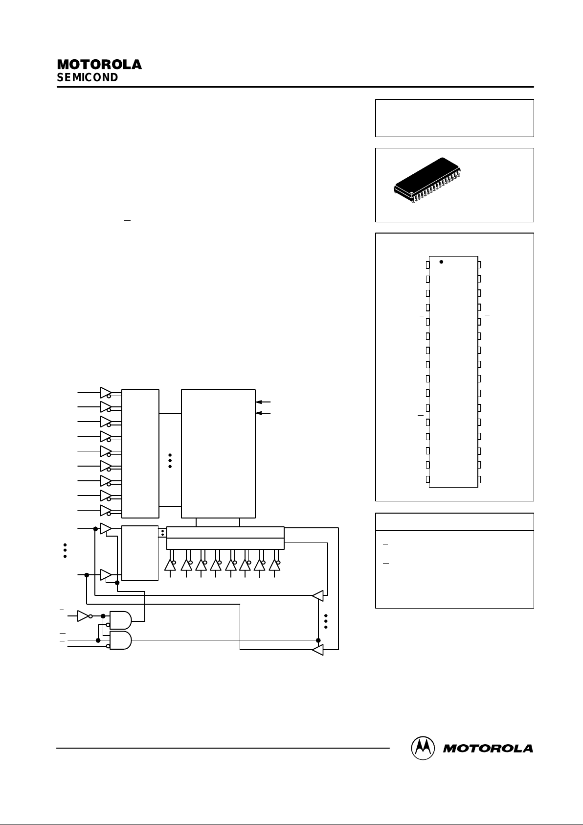
BLOCK DIAGRAM
ROW
DECODER
MEMORY
MATRIX
512 ROWS x 256 x 8
COLUMNS
INPUT
DATA
CONTROL
COLUMN I/O
COLUMN DECODER
A
A
A
A
A
A
A
A
DQ
AA A A
E
W
V
DD
V
SS
A
A A A A
DQ
G
This document contains information on a new product. Motorola reserves the right to change or discontinue this product without notice.
Order this document
by MCM6926A/D
MOTOROLA
SEMICONDUCTOR TECHNICAL DATA
PIN ASSIGNMENT
MCM6926A
WJ PACKAGE
400 MIL SOJ
CASE 857A–02
32
31
30
29
28
27
26
25
24
23
22
21
2
3
1
5
6
4
7
9
10
8
12
13
11
14
20
15
16
19
18
17
A
A
A
E
A
W
A
A
A
V
DD
A
A
A
A
DQ
DQ
A
G
A
A
V
SS
DQ
DQ
AA
A
DQ
DQ
DQ
DQ
A Address Input. . . . . . . . . . . . . . . . . . . . . . .
E
Chip Enable. . . . . . . . . . . . . . . . . . . . . . . .
W
Write Enable. . . . . . . . . . . . . . . . . . . . . . .
G
Output Enable. . . . . . . . . . . . . . . . . . . . .
DQ Data Input/Output. . . . . . . . . . . . . . . . .
V
DD
+ 3.3 V Power Supply. . . . . . . . . . . . .
V
SS
Ground. . . . . . . . . . . . . . . . . . . . . . . . .
PIN NAMES
V
SS
V
DD
REV 1
2/25/97
Motorola, Inc. 1997
MCM6926A
2
MOTOROLA FAST SRAM
TRUTH TABLE (X = Don’t Care)
E G W Mode VDD Current Output Cycle
H X X Not Selected I
SB1
, I
SB2
High–Z —
L H H Output Disabled I
DDA
High–Z —
L L H Read I
DDA
D
out
Read Cycle
L X L Write I
DDA
High–Z Write Cycle
ABSOLUTE MAXIMUM RATINGS (See Note)
Rating
Symbol Value Unit
Power Supply Voltage V
DD
– 0.5 to + 4.6 V
Voltage Relative to VSS for Any Pin
Except V
DD
Vin, V
out
– 0.5 to VDD + 0.5 V
Output Current I
out
± 30 mA
Power Dissipation P
D
0.6 W
Temperature Under Bias T
bias
– 10 to + 85 °C
Operating Temperature T
A
0 to + 70 °C
Storage Temperature — Plastic T
stg
– 55 to + 125 °C
NOTE: Permanent device damage may occur if ABSOLUTE MAXIMUM RATINGS are
exceeded. Functional operation should be restricted to RECOMMENDED OPERATING CONDITIONS. Exposure to higher than recommended voltages for
extended periods of time could affect device reliability.
DC OPERA TING CONDITIONS AND CHARACTERISTICS
(VDD = 3.3 V + 10%, – 5%, TA = 0 to 70°C, Unless Otherwise Noted)
RECOMMENDED OPERATING CONDITIONS
Parameter Symbol Min Typ Max Unit
Supply Voltage (Operating Voltage Range) V
DD
3.135 3.3 3.6 V
Input High Voltage V
IH
2.2 —
VDD + 0.3**
V
Input Low Voltage V
IL
– 0.5*
— 0.8 V
*VIL (min) = – 0.5 V dc; VIL (min) = – 2.0 V ac (pulse width ≤ 2.0 ns) for I ≤ 20.0 mA.
**VIH (max) = VDD + 0.3 V dc; VIH (max) = VDD + 2 V ac (pulse width ≤ 2.0 ns) for I ≤ 20.0 mA.
DC CHARACTERISTICS
Parameter Symbol Min Max Unit
Input Leakage Current (All Inputs, Vin = 0 to VDD) I
lkg(I)
— ± 1.0 µA
Output Leakage Current (E = VIH, V
out
= 0 to VDD) I
lkg(O)
— ± 1.0 µA
Output Low Voltage (IOL = + 8.0 mA) V
OL
— 0.4 V
Output High Voltage (IOH = – 4.0 mA) V
OH
2.4 — V
This device contains circuitry to protect the
inputs against damage due to high static voltages or electric fields; however, it is advised
that normal precautions be taken to avoid
application of any voltage higher than maximum rated voltages to these high–impedance
circuits.
This BiCMOS memory circuit has been designed to meet the dc and ac specifications
shown in the tables, after thermal equilibrium
has been established. The circuit is in a test
socket or mounted on a printed circuit board
and transverse air flow of at least 500 linear feet
per minute is maintained.
MCM6926A
3
MOTOROLA FAST SRAM
POWER SUPPLY CURRENTS (See Note 1)
6926A–8 6926A–10 6926A–12 6926A–15
Parameter Symbol
Typ Max Typ Max Typ Max Typ Max
Unit Notes
AC Active Supply Current
(I
out
= 0 mA) (VDD = max, f = f
max
)
I
DDA
— 150 — 130 — 120 — 110 mA 2, 3, 4
Active Quiescent Current
(E
= VIL, VDD = max, f = 0 MHz)
I
DD2
— 80 — 80 — 80 — 80 mA
AC Standby Current
(E
= VIH, VDD = max, f = f
max
)
I
SB1
— 50 — 45 — 40 — 35 mA 2, 3, 4
CMOS Standby Current
(VDD = max, f = 0 MHz,
E
≥ VDD – 0.2 V,
Vin ≤ VSS + 0.2 V, or ≥ VDD – 0.2 V)
I
SB2
— 20 — 20 — 20 — 20 mA
NOTES:
1. Typical current = 25°C @ 3.3 V.
2. Reference AC Operating Conditions and Characteristics for input and timing (VIH/VIL, tr/tf, pulse level 0 to 3.0 V , VIH = 3.0 V).
3. All address transition simultaneously low (LSB) and then high (MSB).
4. Data states are all zero.
CAPACITANCE (f = 1.0 MHz, dV = 3.0 V, T
A
= 25°C, Periodically Sampled Rather Than 100% Tested)
Parameter Symbol Typ Max Unit
Address Input Capacitance C
in
— 6 pF
Control Pin Input Capacitance C
in
— 6 pF
Input/Output Capacitance C
I/O
— 8 pF
 Loading...