

Motorola MCM67Q909ZP12R Datasheet
MOTOROLA
SEMICONDUCTOR TECHNICAL DATA
Advance Information
512K x 9 Bit Separate I/O
Synchronous Fast Static RAM
The MCM67Q909 is a 4M–bit static random access memory, organized as
512K words of 9 bits. It features separate TTL input and output buffers, which
drive 3.3 V output levels, and incorporates input and output registers on–board
with high speed SRAM. It also features transparent–write and data pass–through
capabilities.
The synchronous design allows for precise cycle control with the use of an
external single clock (K). The addresses (A0 – A18), data input (D0 – D8), data
output (Q0 – Q8), write–enable (W
registered on the rising edge of clock (K).
The control pins (E
, W, G) function dif ferently in comparison to most synchronous SRAMs. This device will not deselect with E
at all times. If E
is registered high, the output pins (Q0 – Q8) will be driven if G
is registered low. The transparent write feature allows the output data to track the
input data. E
, G, and W must be asserted to perform a transparent write (write
and pass–through). The input data is available at the ouputs on the next rising
edge of clock (K).
The pass–through function is always enabled. E
array while allowing a pass–through cycle to occur on the next rising edge of
clock (K). Only a registered G
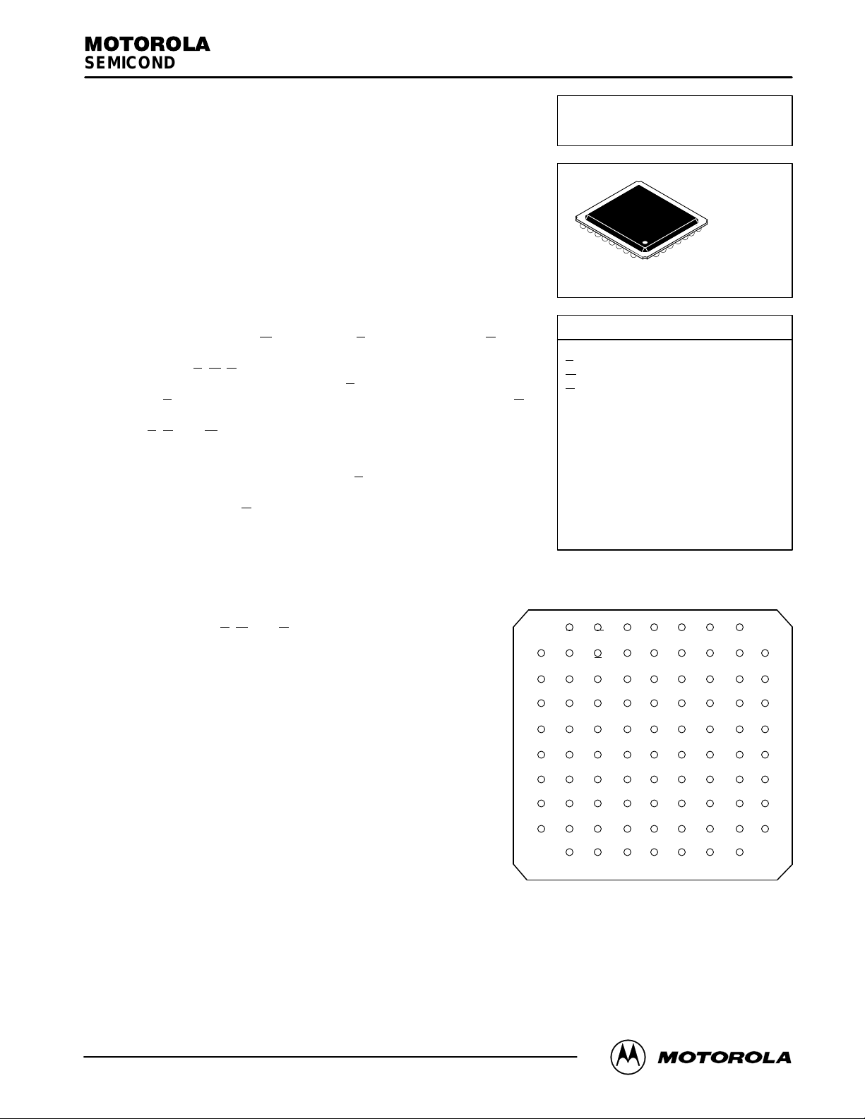
The MCM67Q909 is available in an 86–bump surface mount PBGA (Plastic
Ball Grid Array) package.
• Single 5 V ± 5% Power Supply
• Fast Cycle Time: 12 ns Max
• Single Clock Operation
• TTL Input and Output Levels (Outputs L VTTL Compatible)
• Address, Data Input, E
, W, and G Registers On–Chip
• 83 MHz Maximum Clock Cycle Time
• Self–Timed Write
• Separate Data Input and Output Pins
• Transparent–Write and Pass–Through
• High Output Drive Capability: 50 pF/Output at Rated Access Time
• Boundary Scan Implementation
• PBGA Package for High Speed Operation
), chip–enable (E), and output–enable (G), are
high. The RAM remains active
high disables the write to the
high will three–state the outputs.
A
B
C
D
E
F
G
H
J
K
MCM67Q909
PIN NAMES
A0 – A18 Address Input. . . . . . . . . . . . . . . . .
E
W
G
D0 – D8 Data Inputs. . . . . . . . . . . . . . . . . . . .
Q0 – Q8 Data Outputs. . . . . . . . . . . . . . . . . .
K Clock Input. . . . . . . . . . . . . . . . . . . . . . . . . .
SCK Scan Clock Input. . . . . . . . . . . . . . . . . .
SE Scan Enable. . . . . . . . . . . . . . . . . . . . . . .
SDI Scan Data Input. . . . . . . . . . . . . . . . . . . .
SDO Scan Data Output. . . . . . . . . . . . . . . . .
V
CC
V
SS
NC No Connection. . . . . . . . . . . . . . . . . . . . .
PIN ASSIGNMENT
321
E A4 A0
W
CC
A16 VSSKG
A14
V
V
VSSQ7
D5
V
SS
VCCQ5
Q3D3
VSSD1
A12Q1 A5A8A9V
A17A15D7
V
SS
V
SS
V
SS
V
SS
A18 VSSVSSVSSV
A10
SS
SS
VSSVSSVSSV
VSSVSSVSSV
VSSVSSVSSV
VSSVSSVSSV
SS
SCKA11A13
CC
Order this document
by MCM67Q909/D
86 BUMP PBGA
CASE 896A–02
Chip Enable. . . . . . . . . . . . . . . . . . . . . . . . .
Write Enable. . . . . . . . . . . . . . . . . . . . . . . .
Output Enable. . . . . . . . . . . . . . . . . . . . . .
+ 5 V Power Supply. . . . . . . . . . . . . . .
SDOSDIV
V
SS
A2 D8A6
SS
SS
SS
SS
SS
SS
Ground. . . . . . . . . . . . . . . . . . . . . . . . . .
V
SS
Q8V
V
Q6 D6
V
V
SS
D0
V
A3A7SEV
987654
SS
CC
Q4D4
Q2D2
SS
Q0A1
TOP VIEW
86–BUMP
This document contains information on a new product. Specifications and information herein are subject to change without notice.
REV 3
12/23/97
Motorola, Inc. 1997
MOTOROLA FAST SRAM
Not to Scale
MCM67Q909
1
BLOCK DIAGRAM
A0 – A18
D0 – D8
W
REG
SH
BSR
REG
SH
BSR
E
SH
BSR
G
SH
BSR
SH
BSR
K
REG
REG
REG
DECODERS
MEMORY
ARRAY
512K x 9 ARRAY
SENSE AMPS
AND WRITE
DRIVERS
WRITE PULSE
GENERAT OR
MUX
2:1
OUTPUT
REGISTER
SH
BSR
Q0 – Q8
SH
BSR
*
*
*
NOTES:
1. Bypass mode is entered with SE low and SCK cycled.
2. SH BSR = shadow bypass scan register.
3. 41 bumps used in boundary scan. VSS, VCC, NC, SDI, SDO, SE, and SCK not used in scan path.
4. SDO output sequence: A6, A4, A2, A0, D8, Q8, D6, Q6, D4, Q4, D2, Q2, D0, Q0, A18, A1, A3, A5, A7, A8, A9, A10, A11, A12,
*Four added test pins.
SDI
I
SE
I
SCK
I
A13, Q1, D1, Q3, D3, Q5, D5, Q7, D7, A15, A16, A14, A17, E
LM
LS
SCKSCK
BYPASS
, G, W, K.
SE
1
∧
L
0
SCK
SDO
O
*
MCM67Q909
2
MOTOROLA FAST SRAM
TRUTH TABLE
H
L
X
H
E
(tn)W(tn)G(tn +
L Write and
L L
H Write Valid High–Z I
L Pass–Through Valid D0 – D8 (tn) I
H Pass–Through Don’t Care High–Z I
L Read Don’t Care Q
H Read Don’t Care High–Z I
)
1
Mode
Pass–Through
D0 – D8
(tn)
Valid D0 – D8 (tn) I
Q0 – Q8
(tn + 1)
(tn) I
out
V
CC
Current
CC
CC
CC
CC
CC
CC
ABSOLUTE MAXIMUM RATINGS (See Note)
Rating
Power Supply Voltage V
Voltage Relative to VSS for Any Pin
Except V
Output Current I
Power Dissipation P
Temperature Under Bias T
Operating Temperature T
Storage Temperature — Plastic T
NOTE: Permanent device damage may occur if ABSOLUTE MAXIMUM RATINGS are
CC
exceeded. Functional operation should be restricted to RECOMMENDED OPERATING CONDITIONS. Exposure to higher than recommended voltages for
extended periods of time could affect device reliability.
Symbol Value Unit
CC
Vin, V
out
bias
stg
out
D
A
– 0.5 to + 7.0 V
– 0.5 to VCC + 0.5 V
± 30 mA
1.7 W
– 10 to + 85 °C
0 to + 70 °C
– 55 to + 125 °C
This is a synchronous device. All synchronous inputs must meet specified setup and hold
times with stable logic levels for
edges of clock (K) while the device is selected.
This device contains circuitry to protect the
inputs against damage due to high static voltages or electric fields; however, it is advised
that normal precautions be taken to avoid
application of any voltage higher than maximum rated voltages to these high–impedance
circuits.
ALL
rising
DC OPERA TING CONDITIONS AND CHARACTERISTICS
(VCC = 5.0 V ± 5%, TA = 0 to + 70°C, Unless Otherwise Noted)
RECOMMENDED OPERATING CONDITIONS AND SUPPLY CURRENTS
Parameter Symbol Min Max Unit
Supply Voltage (Operating Voltage Range) V
Input High Voltage V
Input Low Voltage V
Input Leakage Current (All Inputs, Vin = 0 to VCC) I
Output Leakage Current (E = VIH, V
AC Supply Current (I
Output Low Voltage (IOL = + 8.0 mA) V
Output High Voltage (IOH = – 4.0 mA) V
*VIL (min) = – 0.5 V dc; VIL (min) = – 2.0 V ac (pulse width ≤ 20 ns) for I ≤ 20.0 mA.
**VIH (max) = VCC + 0.3 V dc; VIH (max) = VCC + 2.0 V ac (pulse width ≤ 20 ns) for I ≤ 20.0 mA.
= 0 mA) (VCC = max, f = f
out
= 0 to VCC) I
out
) MCM67Q909–12 ns I
max
CC
IH
IL
lkg(I)
lkg(O)
CCA
OL
OH
4.75 5.25 V
2.2 VCC + 0.3** V
– 0.5* 0.8 V
— ± 1.0 µA
— ± 1.0 µA
— 230 mA
— 0.4 V
2.4 3.3 V
MOTOROLA FAST SRAM
MCM67Q909
3
 Loading...