

Motorola MCM6323AYJ10, MCM6323AYJ10A, MCM6323AYJ10AR, MCM6323AYJ10R, MCM6323ATS15AR Datasheet
...
MCM6323A
1
MOTOROLA FAST SRAM
Product Preview
64K x 16 Bit 3.3 V Asynchronous
Fast Static RAM
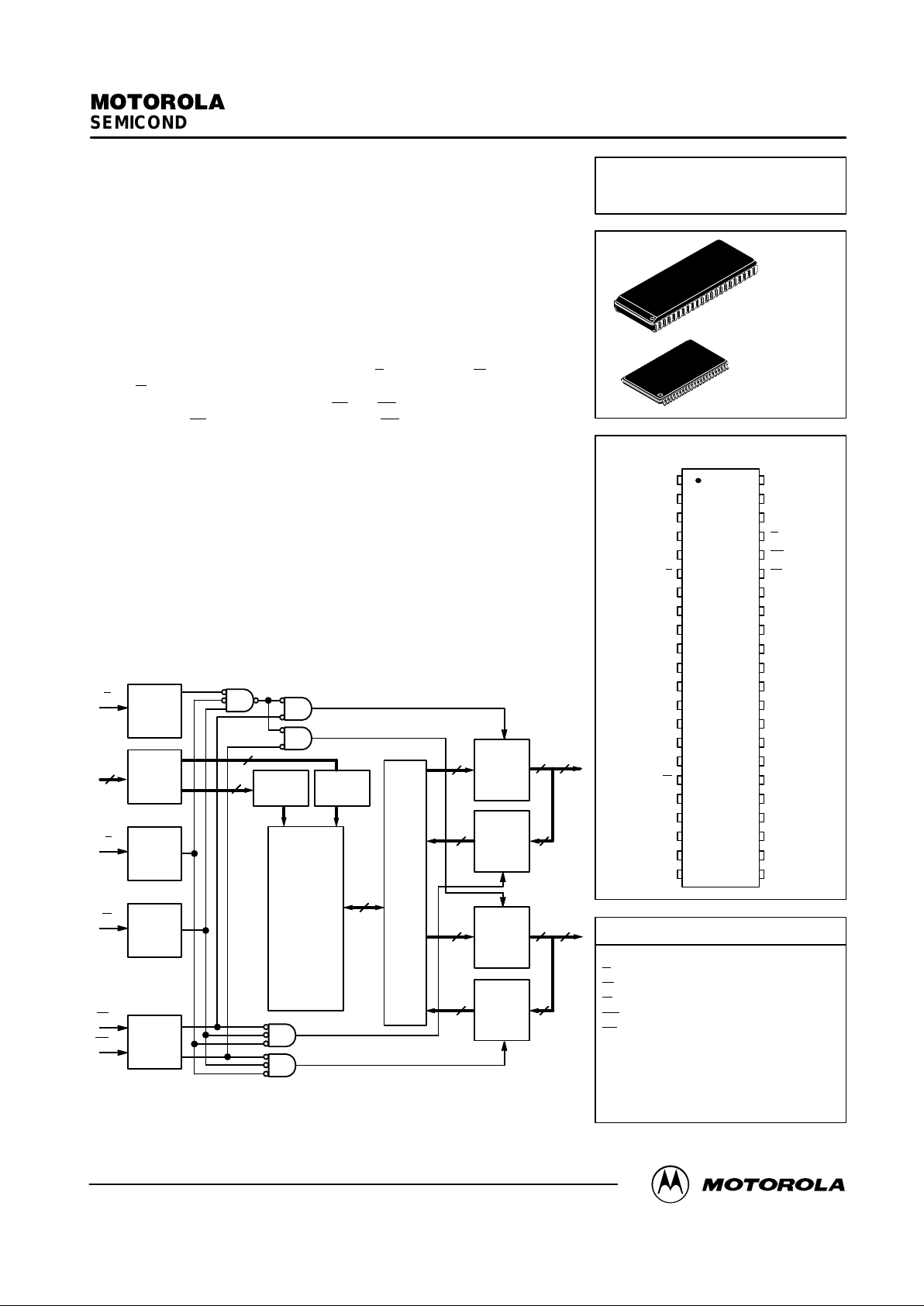
The MCM6323A is a 1,048,576 bit static random access memory organized
as 65,536 words of 16 bits. Static design eliminates the need for external clocks
or timing strobes; CMOS circuitry reduces power consumption and provides for
greater reliability .
The MCM6323A is equipped with chip enable (E
), write enable (W), and output
enable (G
) pins, allowing for greater system flexibility and eliminating bus contention
problems. Separate byte enable controls (LB
and UB) allow individual bytes to be
written and read. LB
controls the 8 DQa bits, while UB controls the 8 DQb bits.
The MCM6323A is available in a 400 mil small–outline J–leaded (SOJ) package and a 44–lead TSOP Type II package in copper leadframe for optimum
printed circuit board (PCB) reliability.
• Single 3.3 V ± 0.3 V Power Supply
• Fast Access Time: 10, 12, 15 ns
• Equal Address and Chip Enable Access Time
• All Inputs and Outputs are TTL Compatible
• Data Byte Control
• Fully Static Operation
• Power Operation: 140/135/130 mA Maximum, Active AC
• Industrial Temperature Option: – 40 to + 85°C
Part Number: SCM6323AYJ10A
BLOCK DIAGRAM
OUTPUT
ENABLE
BUFFER
ADDRESS
BUFFERS
WRITE
ENABLE
BUFFER
BYTE
ENABLE
BUFFER
ROW
DECODER
COLUMN
DECODER
64K x 16
BIT
MEMORY
ARRAY
HIGH
BYTE
OUTPUT
BUFFER
8
HIGH
BYTE
WRITE
DRIVER
LOW
BYTE
OUTPUT
BUFFER
LOW
BYTE
WRITE
DRIVER
SENSE
AMPS
G
W
LB
8
8
8
8
88
8
9
A
CHIP
ENABLE
BUFFER
E
UB
7
HIGH BYTE OUTPUT ENABLE
LOW BYTE OUTPUT ENABLE
HIGH BYTE WRITE ENABLE
LOW BYTE WRITE ENABLE
16
16
8
DQb
8
DQa
This document contains information on a new product under development. Motorola reserves the right
to change or discontinue this product without notice.
Order this document
by MCM6323A/D
MOTOROLA
SEMICONDUCTOR TECHNICAL DATA
MCM6323A
YJ PACKAGE
400 MIL SOJ
CASE 919–01
PIN ASSIGNMENT
A Address Input. . . . . . . . . . . . . . . . . . . . . . . .
E
Chip Enable. . . . . . . . . . . . . . . . . . . . . . . . .
W
Write Enable. . . . . . . . . . . . . . . . . . . . . . . .
G
Output Enable. . . . . . . . . . . . . . . . . . . . . .
UB
Upper Byte. . . . . . . . . . . . . . . . . . . . . . . .
LB
Lower Byte. . . . . . . . . . . . . . . . . . . . . . . . .
DQa Lower Data Input/Output. . . . . . . . . . . .
DQb Upper Data Input/Output. . . . . . . . . . . .
V
DD
+ 3.3 V Power Supply. . . . . . . . . . . . . .
V
SS
Ground. . . . . . . . . . . . . . . . . . . . . . . . . .
NC No Connection. . . . . . . . . . . . . . . . . . . . .
PIN NAMES
5
4
3
2
1
10
9
8
7
6
11
36
37
38
39
40
41
42
35
43
44
34
E
A
A
A
A
DQa
DQa
A
V
DD
DQa
DQa
UB
G
A
A
A
DQb
DQb
DQb
V
SS
DQb
LB
25
26
27
28
29
30
31
24
32
33
23
12
13
14
15
16
17
18
19
20
21
22
DQb
DQb
DQb
DQb
V
DD
A
A
A
NC
A
NCW
DQa
DQa
DQa
V
SS
A
A
DQa
NC
A
A
TS PACKAGE
44–LEAD
TSOP TYPE II
CASE 924A–01
REV 1
10/17/97
Motorola, Inc. 1997
MCM6323A
2
MOTOROLA FAST SRAM
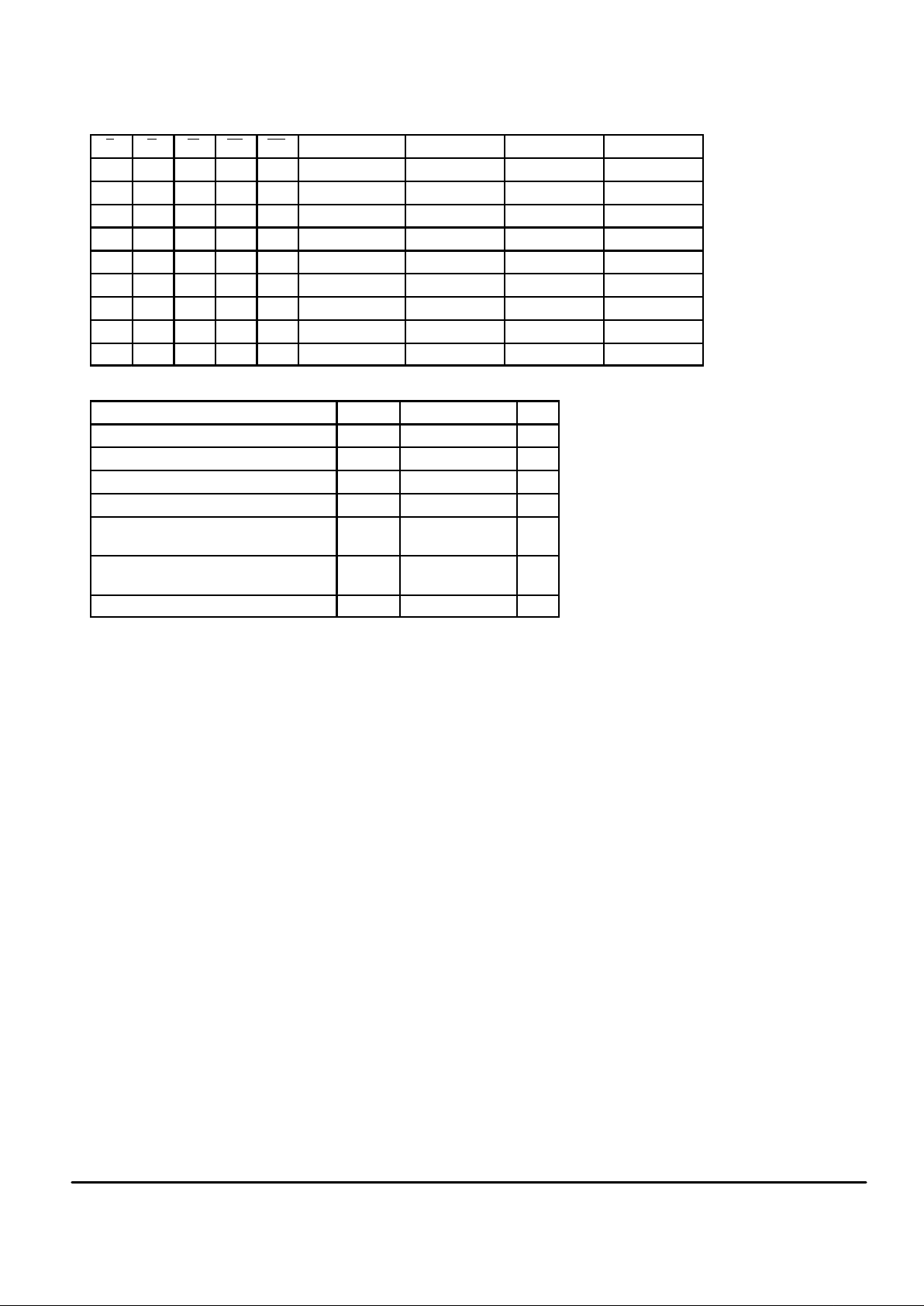
TRUTH TABLE (X = Don’t Care)
E
G W LB UB Mode VDD Current DQa’s DQb’s
H X X X X Not Selected I
SB1
, I
SB2
High–Z High–Z
L H H X X Output Disabled I
DDA
High–Z High–Z
L X X H H Output Disabled I
DDA
High–Z High–Z
L L H L H Low Byte Read I
DDA
D
out
High–Z
L L H H L High Byte Read I
DDA
High–Z D
out
L L H L L Word Read I
DDA
D
out
D
out
L X L L H Low Byte Write I
DDA
D
in
High–Z
L X L H L High Byte Write I
DDA
High–Z D
in
L X L L L Word Write I
DDA
D
in
D
in
ABSOLUTE MAXIMUM RATINGS (See Notes)
Rating
Symbol Value Unit
Supply Voltage V
DD
– 0.5 to + 4.6 V
Voltage on Any Pin V
in
– 0.5 to VDD + 0.5 V
Output Current per Pin I
out
± 20 mA
Package Power Dissipation P
D
.75 W
Temperature Under Bias Commerial
Industrial
T
bias
– 10 to + 85
– 45 to + 90
°C
Operating Temperature Commerial
Industrial
T
A
0 to + 70
– 40 to + 85
°C
Storage Temperature T
stg
– 55 to + 150 °C
NOTES:
1. Permanent device damage may occur if ABSOLUTE MAXIMUM RATINGS are
exceeded. Functional operation should be restricted to RECOMMENDED OPERATING CONDITIONS. Exposure to higher than recommended voltages for extended
periods of time could affect device reliability.
2. All voltages are referenced to VSS.
3. Power dissipation capability will be dependent upon package characteristics and use
environment.
This device contains circuitry to protect the
inputs against damage due to high static voltages or electric fields; however, it is advised
that normal precautions be taken to avoid application of any voltage higher than maximum
rated voltages to these high–impedance circuits.
This CMOS memory circuit has been designed to meet the dc and ac specifications
shown in the tables, after thermal equilibrium
has been established. The circuit is in a test
socket or mounted on a printed circuit board
and transverse air flow of at least 500 linear feet
per minute is maintained.
MCM6323A
3
MOTOROLA FAST SRAM
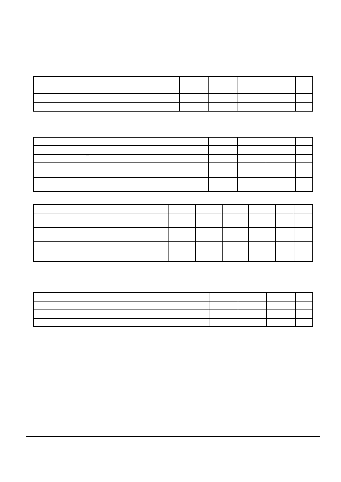
DC OPERA TING CONDITIONS AND CHARACTERISTICS
(VDD = 3.3 V ± 0.3 V, TA = 0 to 70°C, Unless Otherwise Noted)
(TA = – 40 to + 85°C for Industrial Temperature Offering)
RECOMMENDED OPERATING CONDITIONS
Parameter Symbol Min Typ Max Unit
Power Supply Voltage V
DD
3.0 3.3 3.6 V
Input High Voltage V
IH
2.2 —
VDD + 0.3**
V
Input Low Voltage V
IL
– 0.5*
— 0.8 V
*VIL (min) = – 0.5 V dc; VIL (min) = – 2.0 V ac (pulse width ≤ 20 ns) for I ≤ 20.0 mA.
**VIH (max) = VDD + 0.3 V dc; VIH (max) = VDD + 2.0 V ac (pulse width ≤ 20 ns) for I ≤ 20.0 mA.
DC CHARACTERISTICS
Parameter Symbol Min Max Unit
Input Leakage Current (All Inputs, Vin = 0 to VDD) I
lkg(I)
— ± 1.0 µA
Output Leakage Current (E = VIH, V
out
= 0 to VDD) I
lkg(O)
— ± 1.0 µA
Output Low Voltage (IOL = + 4.0 mA)
(IOL = + 100 µA)
V
OL
— 0.4
VSS + 0.2
V
Output High Voltage (IOH = – 4.0 mA)
(IOH = – 100 µA)
V
OH
2.4
VDD – 0.2
— V
POWER SUPPLY CURRENTS (See Note 1)
Parameter
Symbol 6323A–10 6323A–12 6323A–15 Unit Notes
AC Active Supply Current (I
out
= 0 mA) Commerical
(VDD = max, f = f
max
) Industrial
I
DDA
140
150
135
140
130
135
mA 2
AC Standby Current (E = VIH, VDD = max, Commerical
f = f
max
) Industrial
I
SB1
40
45
35
40
30
35
mA 2
CMOS Standby Current (VDD = max, f = 0 MHz, Commerical
E
≥ VDD – 0.2 V , Vin ≤ VSS + 0.2 V, Industrial
or ≥ VDD – 0.2 V)
I
SB2
5
5
5
5
5
5
mA
NOTES:
1. Typical current = 25°C @ 3.3 V.
2. Reference AC Operating Conditions and Characteristics for input and timing (VIH/VIL, tr/tf, pulse level 0 to 3.0 V , VIH = 3.0 V , VIL = 0 V).
CAPACITANCE (f = 1.0 MHz, dV = 3.0 V, T
A
= 25°C, Periodically Sampled Rather Than 100% Tested)
Parameter
Symbol Typ Max Unit
Address Input Capacitance C
in
— 6 pF
Control Input Capacitance C
in
— 6 pF
Input/Output Capacitance C
I/O
— 8 pF
MCM6323A
4
MOTOROLA FAST SRAM
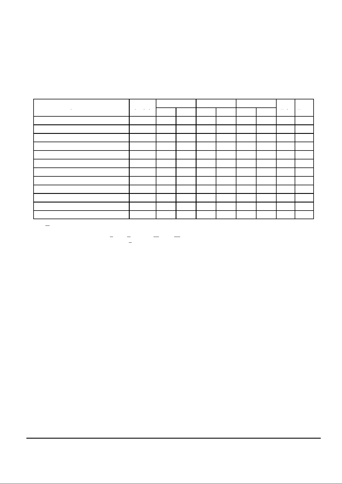
AC OPERA TING CONDITIONS AND CHARACTERISTICS
(VDD = 3.3 V ± 0.3 V, TA = 0 to +70°C, Unless Otherwise Noted)
(TA = – 40 to + 85°C for Industrial Temperature Offering)
Logic Input Timing Measurement Reference Level 1.50 V. . . . . . . .
Logic Input Pulse Levels 0 to 3.0 V. . . . . . . . . . . . . . . . . . . . . . . . . . . .
Input Rise/Fall Time 2 ns. . . . . . . . . . . . . . . . . . . . . . . . . . . . . . . . . . . .
Output Timing Reference Level 1.50 V. . . . . . . . . . . . . . . . . . . . . . . . .
Output Load See Figure 1. . . . . . . . . . . . . . . . . . . . . . . . . . . . . . . . . . . .
READ CYCLE TIMING (See Notes 1, 2, 3, and 4)
MCM6323A–10 MCM6323A–12 MCM6323A–15
Parameter Symbol
Min Max Min Max Min Max
Unit Notes
Read Cycle Time t
AVAV
10 — 12 — 15 — ns 5
Address Access Time t
AVQV
— 10 — 12 — 15 ns
Enable Access Time t
ELQV
— 10 — 12 — 15 ns
Output Enable Access Time t
GLQV
— 4 — 5 — 6 ns 6
Output Hold from Address Change t
AXQX
3 — 3 — 3 — ns
Enable Low to Output Active t
ELQX
3 — 3 — 3 — ns 6, 7, 8
Output Enable Low to Output Active t
GLQX
0 — 0 — 0 — ns 6, 7, 8
Enable High to Output High–Z t
EHQZ
— 4 — 5 — 6 ns 6, 7, 8
Output Enable High to Output High–Z t
GHQZ
— 4 — 5 — 6 ns 6, 7, 8
Byte Enable Access Time t
BLQV
— 4 — 5 — 6 ns
Byte Enable Low to Output Active t
BLQX
0 — 0 — 0 — ns 6, 7, 8
Byte High to Output High–Z t
BHQZ
0 5 0 5 0 5 ns 6, 7, 8
NOTES:
1. W
is high for read cycle.
2. For common I/O applications, minimization, or elimination of bus contention conditions is necessary during read and write cycles.
3. Device is continuously selected (E
= VIL, G = VIL, and LB and/or UB = VIL).
4. Addresses valid prior to or coincident with E
going low.
5. All read cycle timings are referenced from the last valid address to the first transitioning address.
6. Transition is measured 200 mV from steady–state voltage.
7. At any given voltage and temperature, t
EHQZ
(max) < t
ELQX
(min), and t
GHQZ
(max) < t
GLQX
(min), both for a given device and from
device to device.
8. This parameter is sampled and not 100% tested.
 Loading...