

查询MCM6323AYJ10供应商
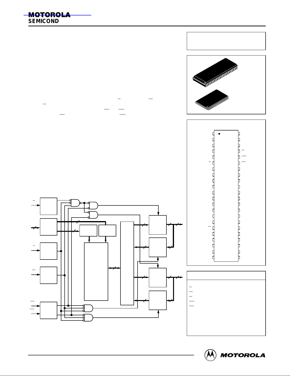
MOTOROLA
SEMICONDUCTOR TECHNICAL DATA
Product Preview
64K x 16 Bit 3.3 V Asynchronous
Fast Static RAM
The MCM6323A is a 1,048,576 bit static random access memory organized
as 65,536 words of 16 bits. Static design eliminates the need for external clocks
or timing strobes; CMOS circuitry reduces power consumption and provides for
greater reliability .
The MCM6323A is equipped with chip enable (E
enable (G
) pins, allowing for greater system flexibility and eliminating bus contention
problems. Separate byte enable controls (LB
written and read. LB
controls the 8 DQa bits, while UB controls the 8 DQb bits.
The MCM6323A is available in a 400 mil small–outline J–leaded (SOJ) package and a 44–lead TSOP Type II package in copper leadframe for optimum
printed circuit board (PCB) reliability.
• Single 3.3 V ± 0.3 V Power Supply
• Fast Access Time: 10, 12, 15 ns
• Equal Address and Chip Enable Access Time
• All Inputs and Outputs are TTL Compatible
• Data Byte Control
• Fully Static Operation
• Power Operation: 140/135/130 mA Maximum, Active AC
• Industrial Temperature Option: – 40 to + 85°C
Part Number: SCM6323A YJ10A
BLOCK DIAGRAM
OUTPUT
G
ENABLE
BUFFER
A
ADDRESS
BUFFERS
16
CHIP
E
ENABLE
BUFFER
WRITE
W
ENABLE
BUFFER
LB
BYTE
ENABLE
UB
BUFFER
This document contains information on a new product under development. Motorola reserves the right
to change or discontinue this product without notice.
7
9
ROW
DECODER
HIGH BYTE OUTPUT ENABLE
LOW BYTE OUTPUT ENABLE
COLUMN
DECODER
64K x 16
BIT
MEMORY
ARRAY
HIGH BYTE WRITE ENABLE
LOW BYTE WRITE ENABLE
), write enable (W), and output
and UB) allow individual bytes to be
HIGH
8
BYTE
OUTPUT
BUFFER
HIGH
8
BYTE
WRITE
DRIVER
SENSE
16
AMPS
LOW
8
BYTE
OUTPUT
BUFFER
LOW
BYTE
WRITE
DRIVER
Order this document
by MCM6323A/D
MCM6323A
YJ PACKAGE
400 MIL SOJ
CASE 919–01
TS PACKAGE
44–LEAD
TSOP TYPE II
CASE 924A–01
PIN ASSIGNMENT
A
1
A
2
A
3
A
4
A
5
6
E
DQa
7
DQa
8
DQa
9
DQa
10
V
11
DD
V
12
SS
DQa
13
DQa
14
DQa
15
8
DQb
8
8
8
DQa
8
A Address Input. . . . . . . . . . . . . . . . . . . . . . . .
E
88
W
G
UB
LB
DQa Lower Data Input/Output. . . . . . . . . . . .
DQb Upper Data Input/Output. . . . . . . . . . . .
V
V
NC No Connection. . . . . . . . . . . . . . . . . . . . .
DD
SS
DQa
A
A
A
A
NC
PIN NAMES
16
17
18
19
20
21
22
+ 3.3 V Power Supply. . . . . . . . . . . . . .
44
43
42
41
40
39
38
37
36
35
34
33
32
31
30
29
28
27
26
25
24
23
Output Enable. . . . . . . . . . . . . . . . . . . . . .
A
A
A
G
UB
LB
DQb
DQb
DQb
DQb
V
SS
V
DD
DQb
DQb
DQb
DQb
NCW
A
A
A
A
NC
Chip Enable. . . . . . . . . . . . . . . . . . . . . . . . .
Write Enable. . . . . . . . . . . . . . . . . . . . . . . .
Upper Byte. . . . . . . . . . . . . . . . . . . . . . . .
Lower Byte. . . . . . . . . . . . . . . . . . . . . . . . .
Ground. . . . . . . . . . . . . . . . . . . . . . . . . .
REV 1
10/17/97
Motorola, Inc. 1997
MOTOROLA FAST SRAM
MCM6323A
1
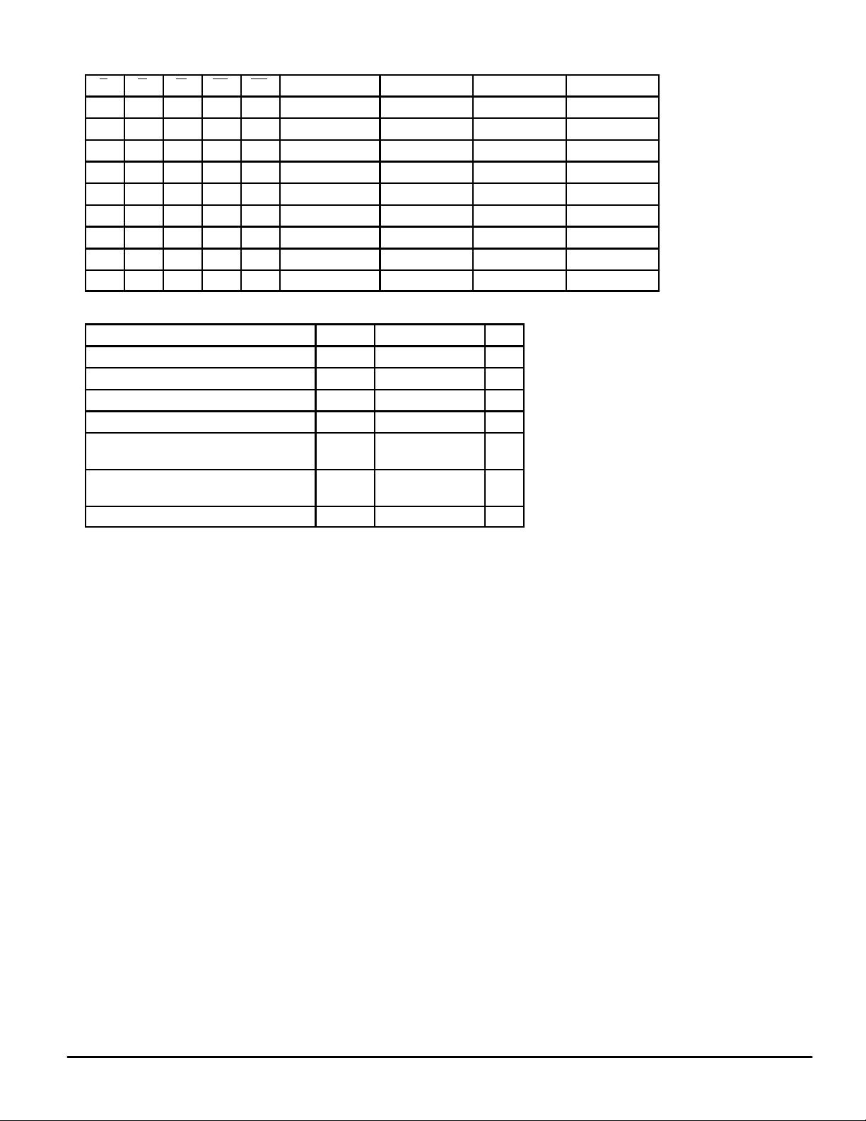
TRUTH TABLE (X = Don’t Care)
G W LB UB Mode VDD Current DQa’s DQb’s
E
H X X X X Not Selected I
L H H X X Output Disabled I
L X X H H Output Disabled I
L L H L H Low Byte Read I
L L H H L High Byte Read I
L L H L L Word Read I
L X L L H Low Byte Write I
L X L H L High Byte Write I
L X L L L Word Write I
SB1
, I
DDA
DDA
DDA
DDA
DDA
DDA
DDA
DDA
SB2
ABSOLUTE MAXIMUM RATINGS (See Notes)
Rating
Supply Voltage V
Voltage on Any Pin V
Output Current per Pin I
Package Power Dissipation P
Temperature Under Bias Commerial
Industrial
Operating Temperature Commerial
Industrial
Storage Temperature T
NOTES:
1. Permanent device damage may occur if ABSOLUTE MAXIMUM RATINGS are
exceeded. Functional operation should be restricted to RECOMMENDED OPERATING CONDITIONS. Exposure to higher than recommended voltages for extended
periods of time could affect device reliability.
2. All voltages are referenced to VSS.
3. Power dissipation capability will be dependent upon package characteristics and use
environment.
Symbol Value Unit
– 0.5 to + 4.6 V
– 0.5 to VDD + 0.5 V
± 20 mA
.75 W
– 10 to + 85
– 45 to + 90
0 to + 70
– 40 to + 85
– 55 to + 150 °C
T
DD
in
out
D
bias
T
A
stg
High–Z High–Z
High–Z High–Z
High–Z High–Z
D
out
High–Z D
D
out
D
in
High–Z D
D
in
°C
°C
High–Z
out
D
out
High–Z
in
D
in
This device contains circuitry to protect the
inputs against damage due to high static voltages or electric fields; however, it is advised
that normal precautions be taken to avoid application of any voltage higher than maximum
rated voltages to these high–impedance circuits.
This CMOS memory circuit has been designed to meet the dc and ac specifications
shown in the tables, after thermal equilibrium
has been established. The circuit is in a test
socket or mounted on a printed circuit board
and transverse air flow of at least 500 linear feet
per minute is maintained.
MCM6323A
2
MOTOROLA FAST SRAM
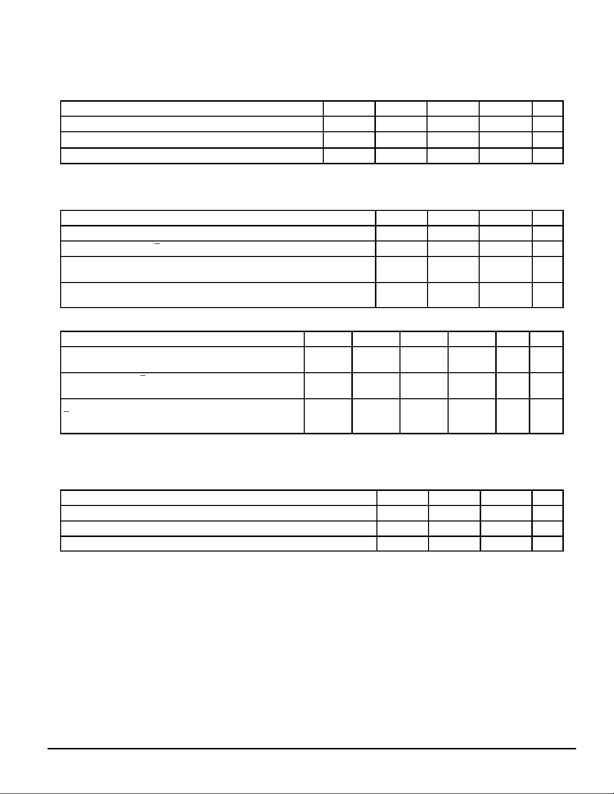
DC OPERA TING CONDITIONS AND CHARACTERISTICS
(VDD = 3.3 V ± 0.3 V, TA = 0 to 70°C, Unless Otherwise Noted)
(TA = – 40 to + 85°C for Industrial Temperature Offering)
RECOMMENDED OPERATING CONDITIONS
Parameter Symbol Min Typ Max Unit
Power Supply Voltage V
Input High Voltage V
Input Low Voltage V
*VIL (min) = – 0.5 V dc; VIL (min) = – 2.0 V ac (pulse width ≤ 20 ns) for I ≤ 20.0 mA.
**VIH (max) = VDD + 0.3 V dc; VIH (max) = VDD + 2.0 V ac (pulse width ≤ 20 ns) for I ≤ 20.0 mA.
DD
IH
IL
DC CHARACTERISTICS
Parameter Symbol Min Max Unit
Input Leakage Current (All Inputs, Vin = 0 to VDD) I
Output Leakage Current (E = VIH, V
Output Low Voltage (IOL = + 4.0 mA)
Output High Voltage (IOH = – 4.0 mA)
= 0 to VDD) I
out
(IOL = + 100 µA)
(IOH = – 100 µA)
POWER SUPPLY CURRENTS (See Note 1)
Parameter
AC Active Supply Current (I
(VDD = max, f = f
AC Standby Current (E = VIH, VDD = max, Commerical
f = f
CMOS Standby Current (VDD = max, f = 0 MHz, Commerical
E
or ≥ VDD – 0.2 V)
NOTES:
) Industrial
max
≥ VDD – 0.2 V, Vin ≤ VSS + 0.2 V, Industrial
1. Typical current = 25°C @ 3.3 V.
2. Reference AC Operating Conditions and Characteristics for input and timing (VIH/VIL, tr/tf, pulse level 0 to 3.0 V, VIH = 3.0 V, VIL = 0 V).
) Industrial
max
= 0 mA) Commerical
out
Symbol 6323A–10 6323A–12 6323A–15 Unit Notes
I
DDA
I
SB1
I
SB2
3.0 3.3 3.6 V
2.2 —
– 0.5*
lkg(I)
lkg(O)
V
V
140
150
40
45
5
5
OL
OH
— 0.8 V
— ± 1.0 µA
— ± 1.0 µA
— 0.4
2.4
VDD – 0.2
135
140
35
40
5
5
VDD + 0.3**
VSS + 0.2
130
135
30
35
5
5
— V
mA 2
mA 2
mA
V
V
CAPACITANCE (f = 1.0 MHz, dV = 3.0 V, T
Address Input Capacitance C
Control Input Capacitance C
Input/Output Capacitance C
= 25°C, Periodically Sampled Rather Than 100% Tested)
A
Parameter
MOTOROLA FAST SRAM
Symbol Typ Max Unit
in
in
I/O
— 6 pF
— 6 pF
— 8 pF
MCM6323A
3
AC OPERA TING CONDITIONS AND CHARACTERISTICS
(VDD = 3.3 V ± 0.3 V, TA = 0 to +70°C, Unless Otherwise Noted)
(TA = – 40 to + 85°C for Industrial Temperature Offering)
Logic Input Timing Measurement Reference Level 1.50 V. . . . . . . .
Logic Input Pulse Levels 0 to 3.0 V. . . . . . . . . . . . . . . . . . . . . . . . . . . .
Input Rise/Fall Time 2 ns. . . . . . . . . . . . . . . . . . . . . . . . . . . . . . . . . . . .
Output Timing Reference Level 1.50 V. . . . . . . . . . . . . . . . . . . . . . . . .
Output Load See Figure 1. . . . . . . . . . . . . . . . . . . . . . . . . . . . . . . . . . . .
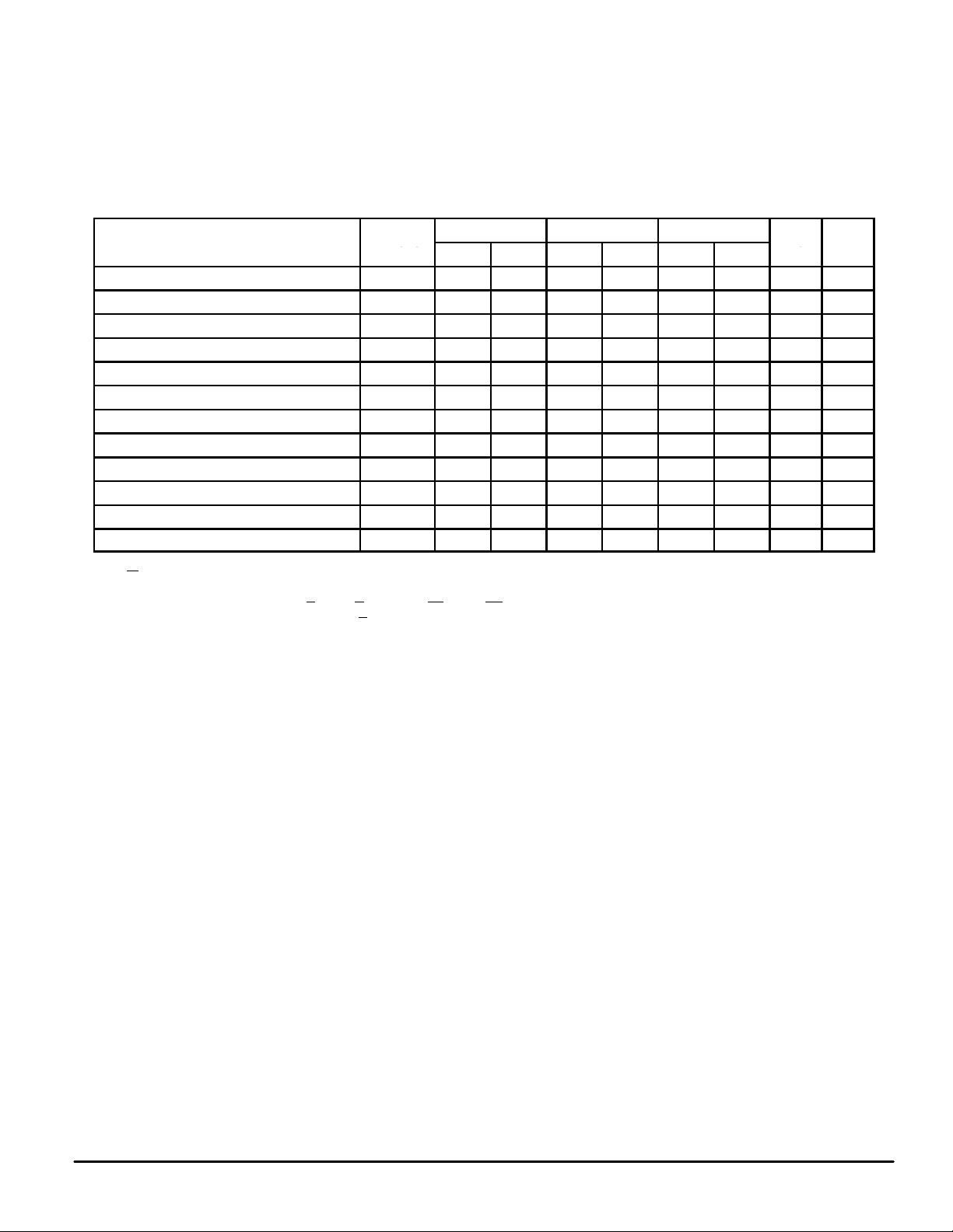
READ CYCLE TIMING (See Notes 1, 2, 3, and 4)
MCM6323A–10 MCM6323A–12 MCM6323A–15
Parameter Symbol
Read Cycle Time t
Address Access Time t
Enable Access Time t
Output Enable Access Time t
Output Hold from Address Change t
Enable Low to Output Active t
Output Enable Low to Output Active t
Enable High to Output High–Z t
Output Enable High to Output High–Z t
Byte Enable Access Time t
Byte Enable Low to Output Active t
Byte High to Output High–Z t
NOTES:
1. W
is high for read cycle.
2. For common I/O applications, minimization, or elimination of bus contention conditions is necessary during read and write cycles.
3. Device is continuously selected (E
4. Addresses valid prior to or coincident with E
5. All read cycle timings are referenced from the last valid address to the first transitioning address.
6. Transition is measured 200 mV from steady–state voltage.
7. At any given voltage and temperature, t
device to device.
8. This parameter is sampled and not 100% tested.
= VIL, G = VIL, and LB and/or UB = VIL).
going low.
EHQZ
AVAV
AVQV
ELQV
GLQV
AXQX
ELQX
GLQX
EHQZ
GHQZ
BLQV
BLQX
BHQZ
(max) < t
Min Max Min Max Min Max
10 — 12 — 15 — ns 5
— 10 — 12 — 15 ns
— 10 — 12 — 15 ns
— 4 — 5 — 6 ns 6
3 — 3 — 3 — ns
3 — 3 — 3 — ns 6, 7, 8
0 — 0 — 0 — ns 6, 7, 8
— 4 — 5 — 6 ns 6, 7, 8
— 4 — 5 — 6 ns 6, 7, 8
— 4 — 5 — 6 ns
0 — 0 — 0 — ns 6, 7, 8
0 5 0 5 0 5 ns 6, 7, 8
ELQX
(min), and t
GHQZ
(max) < t
(min), both for a given device and from
GLQX
Unit Notes
MCM6323A
4
MOTOROLA FAST SRAM

OUTPUT
Z0 = 50
Ω
RL = 50
1.5 V
Figure 1. Equivalent AC T est Load
2.0
1.5
1.0
Ω
30 pF
DELTA TIME DELAY (ns)
+0.3
+0.2
+0.1
–0.1
DELTA TIME DELAY (ns)
0.5
– 0.5
0
100806040200
LUMPED CAPACITANCE, CL (pF)
@ T = 25
°
C, VDD = 3.3 V
OUTPUT
C
L
Figure 2. Lumped Capacitive Load and T ypical Derating Curve
+0.3
+0.2
+0.1
0
DELTA TIME DELAY (ns)
0
–0.1
–0.2
– 0.3
@ T = 25
MOTOROLA FAST SRAM
VDD
– 0.2
3.53.43.33.23.13.0
(V)
3.6 100
°
C
OUTPUT
30 pF
Figure 3. Derating Across T emperature and Voltage
°
C)
T (
@ VDD = 3.3 V
7550250–25–50
MCM6323A
5

A (ADDRESS)
READ CYCLE 1 (See Note 7)
t
AXQX
t
AVAV
Q (DATA OUT)
A (ADDRESS)
E (CHIP ENABLE)
G (OUTPUT ENABLE)
LB, UB (BYTE ENABLE)
t
AVQV
READ CYCLE 2 (See Note 8)
t
AVAV
t
AVQV
t
ELQV
t
ELQX
t
GLQV
t
GLQX
t
BLQV
t
BLQX
DATA VALIDPREVIOUS DATA VALID
t
EHQZ
t
GHQZ
t
BHQZ
Q (DATA OUT)
DATA VALID
MCM6323A
6
MOTOROLA FAST SRAM

WRITE CYCLE 1 (W Controlled, See Notes 1 and 2)
MCM6323A–10 MCM6323A–12 MCM6323A–15
Parameter Symbol
Write Cycle Time t
Address Setup Time t
Address Valid to End of W rite t
Write Pulse Width t
Byte Pulse Width t
Data Valid to End of W rite t
Data Hold Time t
Write Low to Data High–Z t
Write High to Output Active t
Write Recovery Time t
NOTES:
1. A write occurs during the overlap of E
2. For common I/O applications, minimization or elimination of bus contention conditions is necessary during read and write cycles.
3. All write cycle timings are referenced from the last valid address to the first transitioning address.
4. Transition is measured 200 mV from steady–state voltage.
5. At any given voltage and temperature, t
6. This parameter is sampled and not 100% tested.
low, W low, and LB and/or UB low.
WLQZ
AVAV
AVWL
AVWH
WLWH
t
WLEH
BLWH
t
BLEH
DVWH
WHDX
WLQZ
WHQX
WHAX
max < t
Min Max Min Max Min Max
10 — 12 — 15 — ns 3
0 — 0 — 0 — ns
8 — 9 — 10 — ns
,
8 — 9 — 10 — ns
,
8 — 9 — 10 — ns
4 — 5 — 6 — ns
0 — 0 — 0 — ns
0 4 0 5 0 6 ns 4, 5, 6
3 — 3 — 3 — ns 4, 5, 6
0 — 0 — 0 — ns
min both for a given device and from device to device.
WHQX
Unit Notes
A (ADDRESS)
(CHIP ENABLE)
E
(WRITE ENABLE)
W
LB
, UB (BYTE ENABLE)
D (DATA IN)
Q (DATA OUT)
HIGH–Z
t
AVWL
WRITE CYCLE 1
(W Controlled)
t
t
AVWH
t
WLQZ
AVAV
t
WLEH
t
WLWH
t
BLEH
t
BLWH
t
DVWH
DATA VALID
HIGH–Z
t
WHAX
t
WHDX
MOTOROLA FAST SRAM
t
WHQX
MCM6323A
7

WRITE CYCLE 2 (E Controlled, See Notes 1 and 2)
MCM6323A–10 MCM6323A–12 MCM6323A–15
Parameter Symbol
Write Cycle Time t
Address Setup Time t
Address Valid to End of W rite t
Enable to End of Write t
Data Valid to End of W rite t
Data Hold Time t
Write Recovery Time t
NOTES:
1. A write occurs during the overlap of E
2. For common I/O applications, minimization or elimination of bus contention conditions is necessary during read and write cycles.
3. All write cycle timings are referenced from the last valid address to the first transitioning address.
4. If E
goes low coincident with or after W goes low, the output will remain in a high impedance condition.
5. If E
goes high coincident with or before W goes high, the output will remain in a high impedance condition.
low, W low, and LB and/or UB low.
AVAV
AVEL
AVEH
ELEH
t
ELWH
DVEH
EHDX
EHAX
Min Max Min Max Min Max
10 — 12 — 15 — ns 3
0 — 0 — 0 — ns
8 — 9 — 10 — ns
,
8 — 9 — 10 — ns 4, 5
4 — 5 — 6 — ns
0 — 0 — 0 — ns
0 — 0 — 0 — ns
WRITE CYCLE 2
(E Controlled)
Unit Notes
A (ADDRESS)
E (CHIP ENABLE)
(WRITE ENABLE)
W
LB, UB (BYTE ENABLE)
D (DATA IN)
Q (DATA OUT)
t
AVEL
t
t
AVEH
HIGH–Z
AVAV
t
ELEH
t
ELWH
DATA VALID
t
DVEH
t
EHDX
t
EHAX
MCM6323A
8
MOTOROLA FAST SRAM

WRITE CYCLE 3 (B Controlled, See Notes 1 and 2)
MCM6323A–10 MCM6323A–12 MCM6323A–15
Parameter Symbol
Write Cycle Time t
Address Setup Time t
Address Valid to End of W rite t
Write Pulse Width t
Byte Pulse Width t
Data Valid to End of W rite t
Data Hold Time t
Write Low to Data High–Z t
Write High to Output Active t
Write Recovery Time t
NOTES:
1. A write occurs during the overlap of E
2. For common I/O applications, minimization or elimination of bus contention conditions is necessary during read and write cycles.
3. All write cycle timings are referenced from the last valid address to the first transitioning address.
4. Transition is measured 200 mV from steady–state voltage.
5. At any given voltage and temperature, t
6. This parameter is sampled and not 100% tested.
low, W low, and LB and/or UB low.
WLQZ
AVAV
AVBL
AVBH
WLWH
t
WLEH
BLWH
t
BLEH
t
BLBH
DVBH
BHDX
WLQZ
WHQX
BHAX
max < t
Min Max Min Max Min Max
10 — 12 — 15 — ns 3
0 — 0 — 0 — ns
8 — 9 — 10 — ns
,
8 — 9 — 10 — ns
,
8 — 9 — 10 — ns
,
5 — 6 — 7 — ns
0 — 0 — 0 — ns
0 4 0 5 0 6 ns 4, 5, 6
3 — 3 — 3 — ns 4, 5, 6
0 — 0 — 0 — ns
min both for a given device and from device to device.
WHQX
Unit Notes
A (ADDRESS)
(CHIP ENABLE)
E
, UB (BYTE ENABLE)
LB
W
(WRITE ENABLE)
D (DATA IN)
Q (DATA OUT)
HIGH–Z
t
AVBL
WRITE CYCLE 3
(B Controlled)
t
AVAV
t
AVBH
t
WLEH
t
WLWH
t
WLQZ
t
BLEH
t
BLWH
t
BLBH
t
DVBH
DATA VALID
HIGH–Z
t
BHAX
t
BHDX
t
WHQX
MOTOROLA FAST SRAM
MCM6323A
9

ORDERING INFORMATION
(Order by Full Part Number)
Motorola Memory Prefix
Part Number
Full Commercial Part Numbers — MCM6323A YJ10 MCM6323AYJ12 MCM6323AYJ15
Full Industrial Part Numbers — SCM6323AYJ10A SCM6323AYJ12A SCM6323AYJ15A
MCM 6323A YJ XX X
MCM6323A YJ10R MCM6323A YJ12R MCM6323AYJ15R
MCM6323A TS10 MCM6323ATS12 MCM6323ATS15
MCM6323A TS10R MCM6323ATS12R MCM6323ATS15R
SCM6323A YJ10AR SCM6323AYJ12AR SCM6323AYJ15AR
SCM6323A TS10A SCM6323A TS12A SCM6323ATS15A
SCM6323A TS10AR SCM6323ATS12AR SCM6323ATS15AR
X
Shipping Method (R = Tape and Reel,
Blank = Rails for SOJ, Blank = Trays for TSOP)
Temperature (Blank = Commercial, A = Industrial)
Speed (10 = 10 ns, 12 = 12 ns, 15 = 15 ns)
Package (YJ = 400 mil SOJ, TS = 44–Lead
TSOP Type II)
MCM6323A
10
MOTOROLA FAST SRAM

P ACKAGE DIMENSIONS
YJ PACKAGE
400 MIL SOJ
CASE 919–01
A3
SEATING
PLANE
A
44
1
42X
C
A
22 ZONES 2X
e
b44X
0.007 C AB
A2
A1
B0.015
D
b144X
L
0.007 C AB
e
/2
M
E
M
0.007 C AB
E2
VIEW A–A
E2 /2
23
22
44X R
R1
E1
NOTES:
1. DIMENSIONING AND TOLERANCING PER ASME
Y14.5M, 1994.
2. CONTROLLING DIMENSION: INCH.
3. DIMENSION D DOES NOT INCLUDE MOLD FLASH,
TIE BAR BURRS AND GATE BURRS. MOLD
FLASH, TIE BAR BURRS AND GATE BURRS
SHALL NOT EXCEED 0.006 PER END. DIMENSION
E1 DOES NOT INCLUDE INTERLEAD FLASH.
INTERLEAD FLASH SHALL NOT EXCEED 0.010
B
A
A
C0.004
PER SIDE.
4. THE PACKAGE TOP MAY BE SMALLER THAN THE
PACKAGE BOTTOM. DIMENSIONS D AND E1 AND,
HENCE, DATUMS A AND B, ARE DETERMINED AT
THE OUTERMOST EXTREMES OF THE PLASTIC
BODY EXCLUSIVE OF MOLD FLASH, TIE BAR
BURRS, GATE BURRS AND INTERLEAD FLASH,
BUT INCLUDING ANY MISMATCH BETWEEN THE
TOP AND BOTTOM OF THE PLASTIC BODY.
5. DIMENSION b1 DOES NOT INCLUDE DAMBAR
PROTRUSION OR INTRUSION. THE DAMBAR
PROTRUSION(S) SHALL NOT CAUSE THE
SHOULDER WIDTH TO EXCEED b1 MAX BY
MORE THAN 0.005. THE DAMBAR INTRUSION(S)
SHALL NOT REDUCE THE SHOULDER WIDTH TO
LESS THAN 0.001 BELOW b1 MIN.
INCHES
DIM MIN MAX
A 0.128 0.148
A1 0.025 –––
A2 0.082 –––
A3 0.035 0.045
b 0.015 0.020
b1 0.026 0.032
D 1.120 1.130
E 0.435 0.445
E1 0.395 0.405
E2 0.370 BSC
e 0.050 BSC
R1 0.030 0.040
MOTOROLA FAST SRAM
MCM6323A
11

TS PACKAGE
44–LEAD
TSOP TYPE II
CASE 924A–01
B
44 23
VIEW A
E1
AA
122
D1
A
A
A2
22X E
M
0.008 (0.2)C
44X
A
0.004 (0.1) C
SEATING
PLANE
e4X
/2
e
42X
C
A1
L
DETAIL A
ROTATED 90 CLOCKWISE
_
b1
BASE METAL
c1
b
0.008 (0.2) T
SECTION A–A
40 PLACES
NOTES:
1. DIMENSIONING AND TOLERANCING PER ANSI
Y14.5M, 1982.
2. CONTROLLING DIMENSION: INCH.
3. DIMENSION D1 AND E1 DO NOT INCLUDE MOLD
PROTRUSION. ALLOWABLE MOLD PROTRUSION
IS 0.006 (0.015) PER SIDE.
4. DIMENSION b DOES NOT INCLUDE DAMBAR
PROTRUSIONS. DAMBAR PROTRUSIONS SHALL
NOT ALLOW THE b DIMENSION TO EXCEED 0.023
(0.58).
DIM MIN MAX MIN MAX
A ––– 0.050 ––– 1.270
A1 0.002 0.006 0.051 0.152
A2 0.038 0.042 0.965 1.067
b 0.012 0.018 0.305 0.457
b1 0.012 0.016 0.305 0.406
c 0.005 0.008 0.127 0.203
c1 0.004 0.006 0.101 0.152
D1 0.721 0.729 18.313 18.517
e 0.0315 BSC 0.800 BSC
E 0.456 0.470 11.582 11.938
E1 0.396 0.404 10.058 10.262
L 0.016 0.023 0.406 0.584
R1 0.004 REF 0.100 REF
R2 0.004 REF 0.100 REF
q
0 5 0 5
____
M
MILLIMETERSINCHES
R
(R1)
(R2)R
q
c
Z
Motorola reserves the right to make changes without further notice to any products herein. Motorola makes no warranty , representation or guarantee regarding
the suitability of its products for any particular purpose, nor does Motorola assume any liability arising out of the application or use of any product or circuit, and
specifically disclaims any and all liability, including without limitation consequential or incidental damages. “T ypical” parameters which may be provided in Motorola
data sheets and/or specifications can and do vary in different applications and actual performance may vary over time. All operating parameters, including “Typicals”
must be validated for each customer application by customer’s technical experts. Motorola does not convey any license under its patent rights nor the rights of
others. Motorola products are not designed, intended, or authorized for use as components in systems intended for surgical implant into the body, or other
applications intended to support or sustain life, or for any other application in which the failure of the Motorola product could create a situation where personal injury
or death may occur. Should Buyer purchase or use Motorola products for any such unintended or unauthorized application, Buyer shall indemnify and hold Motorola
and its officers, employees, subsidiaries, affiliates, and distributors harmless against all claims, costs, damages, and expenses, and reasonable attorney fees
arising out of, directly or indirectly, any claim of personal injury or death associated with such unintended or unauthorized use, even if such claim alleges that
Motorola was negligent regarding the design or manufacture of the part. Motorola and are registered trademarks of Motorola, Inc. Motorola, Inc. is an Equal
Opportunity/Affirmative Action Employer.
How to reach us:
USA/EUROPE/ Locations Not Listed: Motorola Literature Distribution; JAPAN: Nippon Motorola Ltd.; SPD, Strategic Planning Office; 4-32-1,
P.O. B o x 5405, Denver, Colorado, 80217. 1-303-675-2140 or 1-800-441-2447 Nishi-Gotanda; Shinagawa-ku, T okyo 141, Japan. 81-3-5487-8488
Mfax: RMFAX0@email.sps.mot.com – TOUCHTONE 1-602-244-6609 ASIA/PACIFIC: Motorola Semiconductors H.K. Ltd.; 8B T ai Ping Industrial Park,
Motorola Fax Back System – US & Canada ONLY 1-800-774-1848 51 Ting Kok Road, Tai Po, N.T., Hong Kong. 852-26629298
HOME PAGE: http://motorola.com/sps/ CUSTOMER FOCUS CENTER: 1-800-521-6274
MCM6323A
– http://sps.motorola.com/mfax/
◊
Mfax is a trademark of Motorola, Inc.
MOTOROLA FAST SRAM
MCM6323A/D
12
 Loading...