

Motorola MCM62Y308J17 Datasheet
MCM62Y308
1
MOTOROLA FAST SRAM
Advance Information
Synchronous Line Buffer:
8K x 8 Bit Fast Static Dual
Ported Memory
With IEEE Standard 1149.1 Test Access Port
and Boundary–Scan (JTAG)
The MCM62Y308 is a synchronous, dual ported memory organized as 8,192
words of 8 bits each, fabricated using Motorola’s double–metal, double–poly,
0.65 µm CMOS process. It is intended for high speed video or other applications
which process data on a line–by–line basis. Through the use of a single clock and
port control inputs, separate read and write data ports provide simultaneous access to a common memory array. Simultaneous read/write access to the same
address location is also allowed, with old data being read followed by a write of
the new data. This allows multiple devices to be cascaded with the output of one
directly driving the input of another. In this configuration the data stream can be
tapped a t strategic interconnect p oints t o perform various digital f iltering functions.
Since there are no external address inputs, separate internal read and write
address counters are provided as a means of indexing the memory array. These
counters are preloaded and then selectively incremented or decremented by
asserting read enable (RE) and write enable (WE) inputs, allowing cycle to cycle
control. The a ddress counters can b e reloaded back to their initial values t hrough the
use of the read reload (RR
) and write reload (WR) control inputs. These inputs
initiate the t ransfer o f address r eload register values into t he address counters which
index the memory array. When an address counter reaches 0000 it will roll over on
the n ext c ount. On t he down count the roll o ver c ondition will cause the roll–over flag
(WRF or RRF) to assert high. On the up count these flags must be treated as don’t
cares. The roll–over flag outputs are cleared when their associated roll–over reset
pin i s asserted l ow. T he TDI i nput i s used to write the reload registers using special
test access port instructions.
The read and write address counters are 16 bits long, and only 13 of the 16 bits
are required to index the 8K deep memory array. The remaining three bits are
used for depth expansion. These three bits are compared to the lower three bits
in the control register, and as long as they are equal that port (i.e., read or write)
will remain active. If the bits do not compare, the port will become inactive (i.e.,
for read outputs, high–z; for write inputs, disabled) however, the counter will
continue to count on the rising edge of K as long as the port enable signal (RE or
WE) is asserted. The TDI input is used to write the control register using special
test access port instructions.
The output enable Input can be programmed to be either synchronous or
asynchronous through the control register.
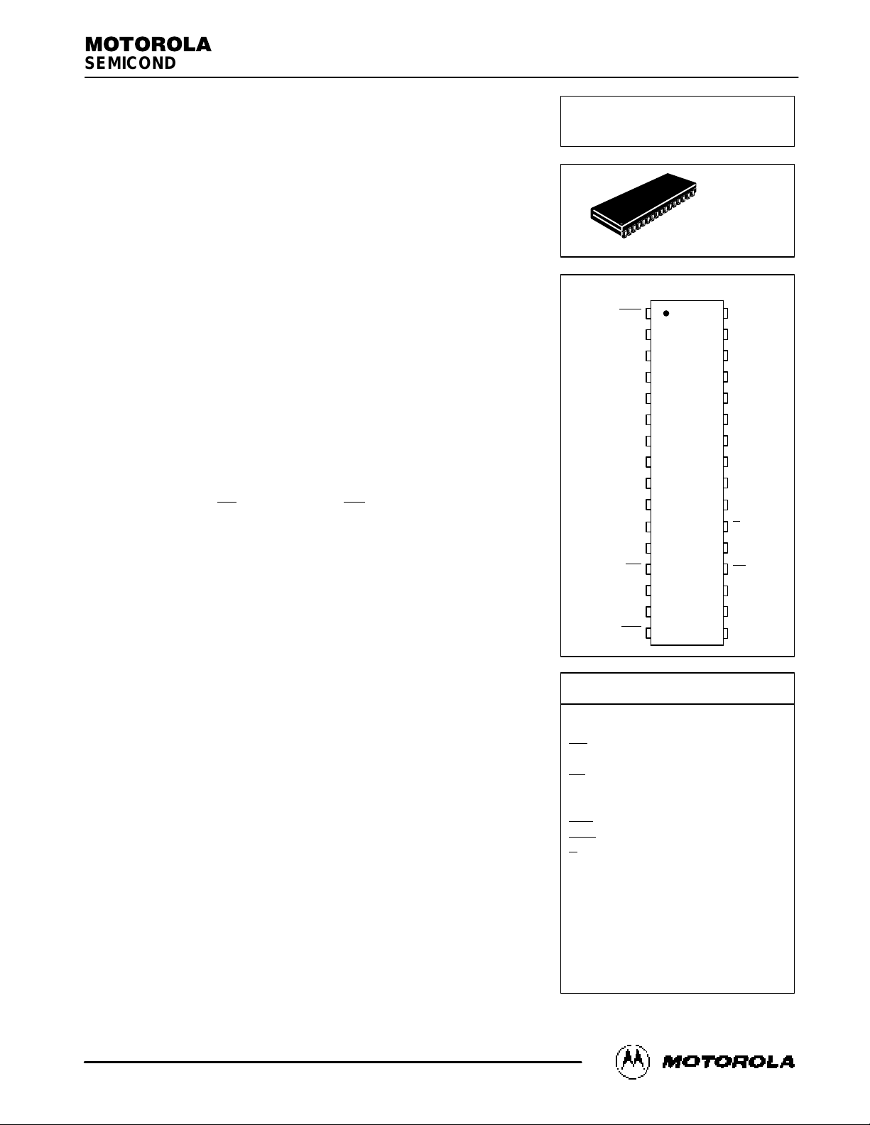
The MCM62Y308 is available in a 32 pin SOJ package.
• 8K x 8 Fast Access Static Memory Array
• Single 5 V Power Supply —MCM62Y308–17: ± 5%
• Synchronous, Simultaneous Read/Write Memory Access
• 50 MHz Maximum Clock Cycle Time, < 15 ns Read Access
• Single Clock Operation
• Separate Read/Write Address Counters with Reload Control
• Separate Up/Down Counter Control for Both Read and Write
• Separate Roll–Over Flag Outputs for Read and Write
• Programmable Output Enable Control (Synchronous or Asynchronous)
• Cascadable I/O Interface
• IEEE Standard 1149.1 Test Port (JTAG)
• Expand ID Register for Depth Expansion
• High Board Density SOJ Package
This document contains information on a new product under development. Motorola reserves the right to change or discontinue this product without notice.
Order this document
by MCM62Y308/D
MOTOROLA
SEMICONDUCTOR TECHNICAL DATA
MCM62Y308
J PACKAGE
300 MIL SOJ
CASE 857–02
PIN ASSIGNMENT
5
4
3
2
1
10
9
8
7
6
11
12
13
14
20
21
22
23
24
25
26
19
27
28
18
17
D1
D4
D5
D6
D7
WE
D0
D3
TCK
TDI
WR
D2
V
DD
K
Q3
Q4
Q5
Q6
Q7
TDO
RR
RE
TMS
V
SS
Q1
Q2
G
Q0
PIN NAMES
K Clock Input. . . . . . . . . . . . . . . . . . . . . . . . . .
WE Write Enable Input. . . . . . . . . . . . . . . . . .
WR
Write Address Reload Input. . . . . . . . . .
RE .Read Enable Input. . . . . . . . . . . . . . . . .
RR
Read Address Reload Input. . . . . . . . .
RRF Read Roll–Over Flag Output. . . . . . . .
WRF Write Roll–Over Flag Output. . . . . . .
RRR
Read Roll–Over Reset Input. . . . . . . .
WRR
Write Roll–Over Reset Input. . . . . . .
G
Output Enable Input. . . . . . . . . . . . . . . . .
D0 – D7 Data Inputs. . . . . . . . . . . . . . . . . . . .
Q0 – Q7 Data Outputs. . . . . . . . . . . . . . . . . .
TCK Test Clock Input. . . . . . . . . . . . . . . . . . .
TMS Test Mode Select. . . . . . . . . . . . . . . . . .
TDI Test Data Input. . . . . . . . . . . . . . . . . . . .
TDO Test Data Output. . . . . . . . . . . . . . . . . .
V
DD
+ 5 V Power Supply. . . . . . . . . . . . . . .
V
SS
Ground. . . . . . . . . . . . . . . . . . . . . . . . . .
32
1
15
16
29
30
31
32WRR
RRR
RRF
WRF
REV 2
5/95
Motorola, Inc. 1994
MCM62Y308
2
MOTOROLA FAST SRAM
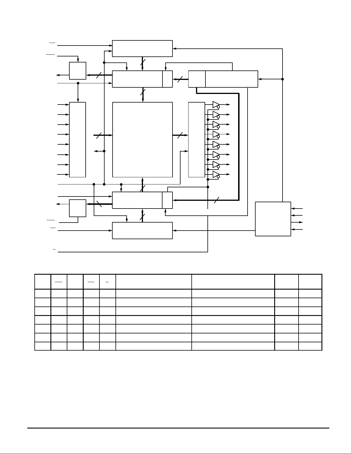
BLOCK DIAGRAM
WRITE RELOAD REGISTER
WRITE COUNTER
8K x 8 STATIC
MEMORY ARRAY
READ COUNTER
READ RELOAD REGISTER
INPUT REGISTER
OUTPUT LATCH
EXP ID CONTROL REGISTER
K
RE
G
RR
16
13
13
16
3
3
8
TMS
TCK
TDO
TDI
WR
WE
EXP. ID
COMPARE
TEST ACCESS
PORT
UP/DOWN AND CLEAR/RELOAD CONTROL
8
Q0
Q1
Q2
Q3
Q4
Q5
Q6
Q7
D0
D1
D2
D3
D4
D5
D6
D7
UP/DOWN AND CLEAR/RELOAD CONTROL
WRF
WRR
16
RRF
RRR
16
TRUTH TABLE (X = Don’t Care)
WE
WR RE RR G Match EXP ID (Read/Write) Mode (Read/Write)
Supply
Current
Q0 – 7
Status
X L X L L Match Read/Match Write Reload, Read/Reload, Write Disable I
CC
Data Out
H H H H L Match Read/Match Write Count, Read/Write, Count I
CC
Data Out
L H L H L Match Read/Match Write Read Count Disable/Write Disable I
CC
Data Out
H H H H H Match Read/Match Write Count, Read/Write, Count I
CC
High–Z
H H H H X No Match Read/No Match Write Count, No Read/No Write, Count I
SB
High–Z
H H H H X No Match Read/Match Write Count, No Read/Write, Count I
SB
High–Z
H H H H L Match Read/No Match Write Count, Read/No Write, Count I
CC
Data Out
MCM62Y308
3
MOTOROLA FAST SRAM
PIN DESCRIPTIONS
SOJ Pin Locations Symbol
Type Description
11 K Input CLOCK – System clock input pin accepting a minimum 8 ns clock high
or clock low pulse at a minimum 20 ns clock cycle. All other
synchronous inputs excluding the test access port are captured on the
rising edge of this signal.
12 WE Input WRITE ENABLE – Write enable is captured on K leading edge. When
asserted this causes the input data D0 – D7 to be written into the RAM
address controlled by the write address counter and increments the
counter for the next write.
21 RE Input READ ENABLE – Read enable is captured on K leading edge. When
asserted increments the counter for the next read operation. This
causes a RAM read access from address controlled by the read
address counter to be inserted in the output register Q0 – Q7.
13 WR Input WRITE RELOAD – Write reload is captured on K leading edge. When
asserted this causes the write address counter to be initialized to the
contents of the write reload register or “cleared” as specified by control
register bit 3. See control register bit 3 for “cleared” description.
20 RR Input READ RELOAD – Read reload is captured on K leading edge. When
asserted this causes the read address counter to be initialized to the
contents of the read reload register or “cleared” as specified by control
register bit 5. See control register bit 5 for “cleared” description.
22 G Input OUTPUT ENABLE – When asserted low causes the outputs Q0 – Q7
to become active and when deasserted high causes them to High–Z.
This pin can be either synchronous with K leading edge or
asynchronous as specified by control register bit 7.
9, 8, 7, 6, 5, 4, 3, 2 D0 – D7 Input DATA INPUT – The levels on these pins are captured on the K leading
edge. The value captured will be written into the RAM if WE is also
asserted and the expand ID bits match the upper three bits of the write
address counter.
24, 25, 26, 27, 28, 29, 30, 31 Q0 – Q7 Output DATA OUTPUT – Data outputs are available from the read output
register < 15 ns from the rising edge of K when RE or RR
is asserted.
outputs are disabled when the upper three bits of the read address
counter do not match the three expand ID bits of the control register.
G
will also control the disabling of the outputs either synchronously or
asynchronously. See G
description.
17, 32 RRF, WRF Output ROLL–OVER FLAG – These signals are asserted high on the clock
cycle where the address counters (write address counter for WRF and
read address counter for RRF) roll–over to 0000 during count down.
During count up these pins must be treated as don’t cares.
16, 1 RRR, WRR Input ROLL–OVER RESET – The level on these pins is captured on the K
leading edge. When asserted low, each will reset their associated
roll–over flag output.
TEST ACCESS PORT PIN DESCRIPTIONS (The Test Access Port Conforms with the IEEE Standard 1149.1. It is also Used
to Load Device Specific Registers Used to Configure the MCM62Y308.)
SOJ Pin Locations Symbol
Type Description
15 TCK Input
TEST CLOCK – Samples and clocks all TAP events. All inputs are
captured on TCK rising edge and all outputs propagate from TCK falling
edge. It also can take the place of K in device operation in certain test
conditions.
18 TMS Input TEST MODE SELECT – Sampled on the rising edge of TCK.
Determines the movement through the TAP state machine (Figure 2).
This circuit is designed in such a way that an undriven input will
produce a response identical to the application of a logic 1.
14 TDI Input TEST DATA IN – Sampled on the rising edge of TCK. This is the input
side of the serial register placed between TDI and TDO. The register
placed between TDI and TDO is determined by the state of the TAP
state machine and what instruction is active in the TAP instruction
register. This circuit is designed in such a way that an undriven input
will produce a response identical to the application of a logic 1.
19 TDO Output TEST DATA OUT – Output that is active depending on the state of the
TAP state machine. Output changes off the trailing edge of TCK. This is
the output side of the serial register placed between TDI and TDO.
MCM62Y308
4
MOTOROLA FAST SRAM
MAXIMUM RATINGS* (Voltages Referenced to V
SS
= 0)
Rating
Symbol Value Unit
Power Supply Voltage V
DD
– 0.5 to + 7.0 V
Voltage Relative to V
SS
Vin, V
out
– 0.5 to VDD + 0.5 V
Output Current (per I/O) I
out
± 20 mA
Power Dissipation P
D
1.0 W
Temperature Under Bias T
bias
– 10 to + 85 °C
Operating Temperature T
A
0 to + 70 °C
Storage Temperature T
stg
– 55 to + 125 °C
NOTE: Permanent device damage may occur if ABSOLUTE MAXIMUM RATINGS are
exceeded. Functional operation should be restricted to RECOMMENDED OPERATING CONDITIONS. Exposure to higher than recommended voltages for
extended periods of time could affect device reliability.
DC OPERATING CONDITIONS AND CHARACTERISITICS
(TA = 0 to 70 °C, Unless Otherwise Noted)
RECOMMENDED OPERATING CONDITIONS (Voltages referenced to V
SS
= 0 V)
Parameter
Symbol Min Typ Max Unit
Supply Voltage (Operating Voltage Range) MCM62Y308–17
VDD4.75
5.0
5.25
V
Input High Voltage V
IH
2.2 — VDD + 0.3 V
Input Low Voltage V
IL
– 0.5* — 0.8 V
*VIL (min) = – 3.0 V ac (pulse width ≤ 20 ns)
DC CHARACTERISTICS AND SUPPLY CURRENTS
Parameter Symbol Min Max Unit
Input Leakage Current (All Inputs, Vin = 0 to VDD) I
lkg(I)
± 1.0 µA
Output Leakage Current (G = VIH, V
out
= 0 to VDD) I
lkg(O)
± 1.0 µA
AC Supply Current (G = VIH, I
out
= 0 mA, All Inputs ≥ VIL = 0.0 V and VIH ≥ 3.0,
Cycle Time = 20 ns)
I
CCA
150 mA
AC Standby Current (When Expand ID Bits Do Not Match the Read Address Counter,
Cycle Time = 20 ns)
I
SB
100 mA
Output Low Voltage (IOL = + 4.0 mA) V
OL
0.4 V
Output High Voltage (IOH = – 4.0 mA) V
OH
2.4 V
CAPACITANCE (f = 1.0 MHz, dV = 3.0 V, T
A
= 25°C, Periodically Sampled Rather Than 100% Tested)
Characteristic
Symbol Typ Max Unit
Input Capacitance C
in
4 6 pF
Output Capacitance (Q0 – Q7, TDO, WRF, RRF) C
out
6 8 pF
This device contains circuitry to protect the
inputs against damage due to high static voltages or electric fields; however, it is advised
that normal precautions be taken to avoid
application of any voltage higher than maximum rated voltages to this high–impedance
circuit.
MCM62Y308
5
MOTOROLA FAST SRAM
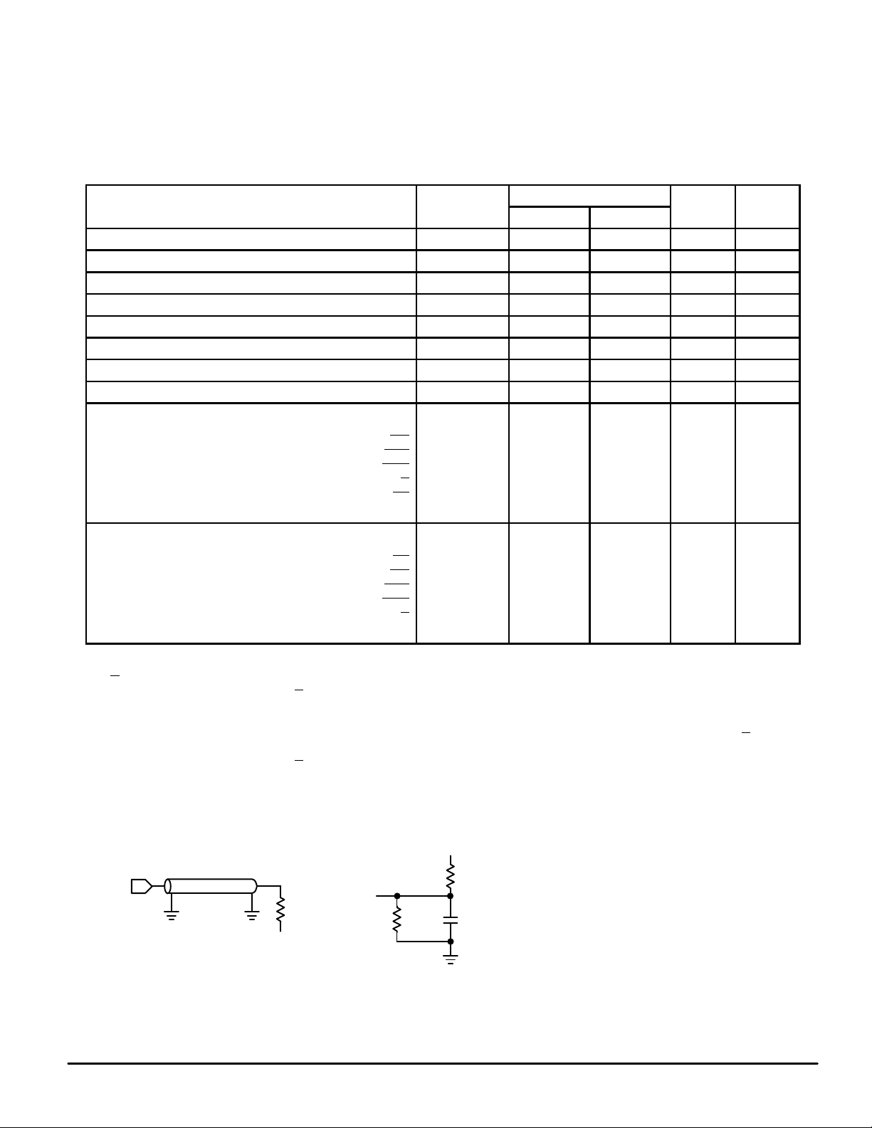
AC OPERATING CONDITIONS AND CHARACTERISTICS
(TA = 0 to + 70°C, Unless Otherwise Noted)
Input Pulse Levels 0 to 3.0 V. . . . . . . . . . . . . . . . . . . . . . . . . . . . . . . . .
Input Rise/Fall Time 3 ns. . . . . . . . . . . . . . . . . . . . . . . . . . . . . . . . . . . .
Input Timing Measurement Reference Level 1.5 V. . . . . . . . . . . . . . .
Output Timing Reference Level 1.5 V. . . . . . . . . . . . . . . . . . . . . . . . . .
Output Load Terminated 50 Ohm Transmission Line. . . . . . . . . . . . .
READ/WRITE CYCLE TIMING
MCM62Y308–17
Parameter Symbol Min Max Unit Notes
Cycle Time t
KHKH
22 — ns
Clock High Time t
KHKL
9 — ns
Clock Low Time t
KLKH
9 — ns
Clock High to Output Valid t
KHQV
5 17 ns
Clock High to Roll–Over Flag Valid t
KHRFV
5 11 ns
Clock High to Output High–Z t
KHQZ
5 15 ns 1
Output Enable Low to Output Valid t
GLQV
3 10 ns 2, 4
Output Enable High to Output High–Z t
GHQZ
0 5 ns 2, 3, 4
Setup Times: RE
WE
WR
RRR
WRR
G
RR
Data In
t
REVKH
t
WEVKH
t
WRVKH
t
RRRVKH
t
WRRVKH
t
GVKH
t
RRVKH
t
DVKH
2
3
1
—
—
—
ns 5
6
5
Hold Times: RE
WE
RR
WR
RRR
WRR
G
Data In
t
KHREX
t
KHWEX
t
KHRRX
t
KHWRX
t
KHRRRX
t
KHWRRX
t
KHGX
t
KHDX
2 — ns 5
6
NOTES:
1. The outputs High–Z from a clock high edge when the upper three bits of the Read Address Counter do not match the 3 ID Expansion bits.
2. G
is a don’t care when the three ID expansion bits do not match the upper three bits of the Read Address Counter.
3. t
GLQV
and t
GHQZ
only apply when G
is programmed as Asynchronous. (See TAP LDCONT instruction.)
4. Transition is measured ± 500 mV from steady–state voltage. This parameter is sampled and not 100% tested. At any given voltage and
temperature, t
GHQZ
max is less than t
GLQV
min for a given device and from device to device.
5. This is a synchronous device. All inputs must meet the specified setup and hold times for
ALL
rising edges of Clock except for G when it is
programmed to be asynchronous.
6. t
GVKH
and t
KHGX
only apply when G
is programmed as synchronous.
AC TEST LOADS
Figure 1A Figure 1B
The table of timing values shows either a
minimum or a maximum limit for each parameter. Input requirements are specified from
the external system point of view. Thus, address setup time is shown as a minimum
since the system must supply at least that
much time (even though most devices do not
require it). On the other hand, responses from
the memory are specified from the device
point of view. Thus, the access time is shown
as a maximum since the device never provides data later than that time.
TIMING LIMITS
OUTPUT
Z0 = 50
Ω
RL = 50
Ω
VL = 1.5 V
5 pF
+ 5 V
OUTPUT
255
Ω
480
Ω
 Loading...