

MOTOROLA MC74VHC573ML2, MC74VHC573DWR2, MC74VHC573M, MC74VHC573MEL, MC74VHC573ML1 Datasheet
...
Semiconductor Components Industries, LLC, 2000
April, 2000 – Rev. 3
1 Publication Order Number:
MC74VHC573/D
MC74VHC573
Octal D-Type Latch with
3-State Output
The MC74VHC573 is an advanced high speed CMOS octal latch
with 3–state output fabricated with silicon gate CMOS technology. It
achieves high speed operation similar to equivalent Bipolar Schottky
TTL while maintaining CMOS low power dissipation.
This 8–bit D–type latch is controlled by a latch enable input and an
output enable input. When the output enable input is high, the eight
outputs are in a high impedance state.
The internal circuit is composed of three stages, including a buffer
output which provides high noise immunity and stable output. The
inputs tolerate voltages up to 7V, allowing the interface of 5V systems
to 3V systems.
• High Speed: t
PD
= 4.5ns (Typ) at VCC = 5V
• Low Power Dissipation: I
CC
= 4µA (Max) at TA = 25°C
• High Noise Immunity: V
NIH
= V
NIL
= 28% V
CC
• Power Down Protection Provided on Inputs
• Balanced Propagation Delays
• Designed for 2V to 5.5V Operating Range
• Low Noise: V
OLP
= 1.2V (Max)
• Pin and Function Compatible with Other Standard Logic Families
• Latchup Performance Exceeds 300mA
• ESD Performance: HBM > 2000V ; Machine Model > 200V
• Chip Complexity: 218 FETs or 54.5 Equivalent Gates
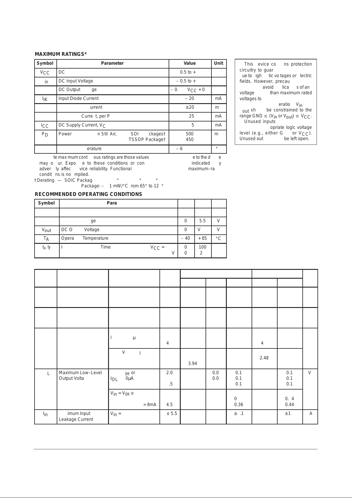
LOGIC DIAGRAM
DATA
INPUTS
D0
D1
D2
D3
D4
D5
D6
D7
LE
OE
11
1
9
8
7
6
5
4
3
219
18
17
16
15
14
13
12
Q0
Q1
Q2
Q3
Q4
Q5
Q6
Q7
NONINVERTING
OUTPUTS
OE LE Q
L
L
L
H
H
H
L
X
H
L
No Change
Z
INPUTS OUTPUT
FUNCTION TABLE
D
H
L
X
X
http://onsemi.com
MARKING
DIAGRAMS
1
20
A = Assembly Location
WL = Wafer Lot
YY = Year
WW = Work Week
SOIC–20 WIDE
DW SUFFIX
CASE 751D
VHC573
AWLYYWW
SOIC EIAJ
M SUFFIX
CASE 967
1
20
VHC573
AWLYYWW
TSSOP–20
DT SUFFIX
CASE 948E
1
20
1
20
1
20
Device Package Shipping
ORDERING INFORMATION
MC74VHC573M SOIC EIAJ 40 / Rail
MC74VHC573DW SOIC–WIDE
38 / Rail
MC74VHC573DWR2 SOIC–WIDE 1000 / Reel
MC74VHC573DT TSSOP–20 75 / Rail
MC74VHC573DTR2 TSSOP–20
2500 / Reel
VHC
573
ALYW
1
20
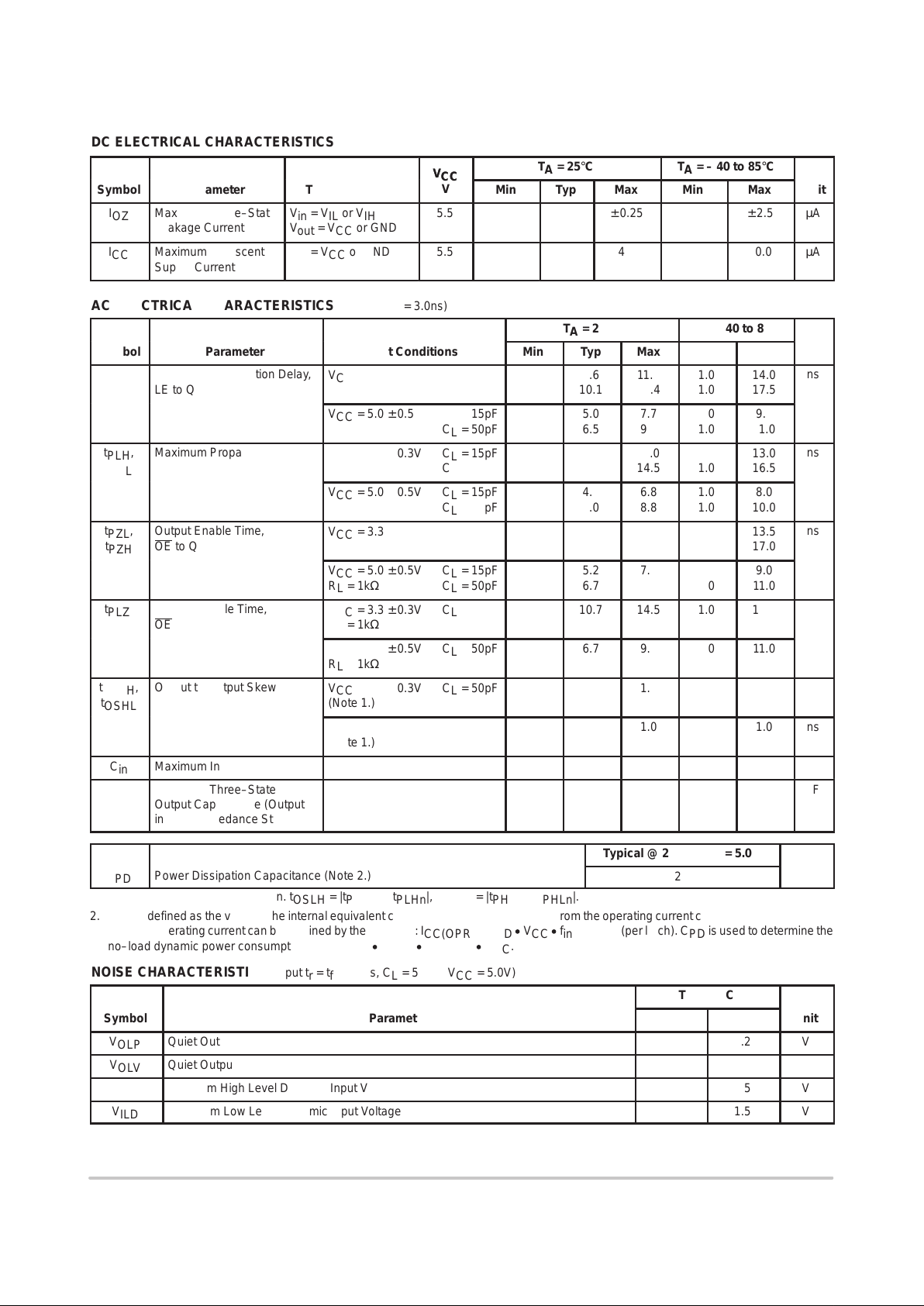
PIN ASSIGNMENT
D4
D2
D1
D0
OE
GND
D7
D6
D5
D3 5
4
3
2
1
10
9
8
7
6
14
15
16
17
18
19
20
11
12
13
Q3
Q2
Q1
Q0
V
CC
LE
Q7
Q6
Q5
Q4
MC74VHC573MEL SOIC EIAJ 2000 / Reel
MC74VHC573
http://onsemi.com
2
MAXIMUM RATINGS*
Symbol
Parameter
Value
Unit
V
CC
DC Supply Voltage
– 0.5 to + 7.0
V
V
in
DC Input Voltage
– 0.5 to + 7.0
V
V
out
DC Output Voltage
– 0.5 to VCC + 0.5
V
I
IK
Input Diode Current
– 20
mA
I
OK
Output Diode Current
± 20
mA
I
out
DC Output Current, per Pin
± 25
mA
I
CC
DC Supply Current, VCC and GND Pins
± 75
mA
ÎÎ
Î
P
D
ОООООООООООО
Î
Power Dissipation in Still Air, SOIC Packages†
TSSOP Package†
ÎÎÎ
Î
500
450
Î
Î
mW
T
stg
Storage Temperature
– 65 to + 150
_
C
* Absolute maximum continuous ratings are those values beyond which damage to the device
may occur. Exposure to these conditions or conditions beyond those indicated may
adversely affect device reliability. Functional operation under absolute–maximum–rated
conditions is not implied.
†Derating — SOIC Packages: – 7 mW/_C from 65_ to 125_C
TSSOP Package: – 6.1 mW/_C from 65_ to 125_C
RECOMMENDED OPERATING CONDITIONS
Symbol
Parameter
Min
ÎÎ
Max
Unit
V
CC
DC Supply Voltage
2.0
ÎÎ
5.5
V
V
in
DC Input Voltage
0
ÎÎ
5.5
V
V
out
DC Output Voltage
0
ÎÎ
V
CC
V
T
A
Operating Temperature
– 40
ÎÎ
+ 85
_
C
tr, t
f
Input Rise and Fall Time VCC = 3.3V
VCC = 5.0V00
ÎÎ
10020ns/V
DC ELECTRICAL CHARACTERISTICS
V
TA = 25°C
TA = – 40 to 85°C
Symbol
Parameter
Test Conditions
V
CC
V
Min
Typ
Max
Min
Max
Unit
ÎÎ
Î
V
IH
ООООО
Î
Minimum High–Level
Input Voltage
ОООООÎÎ
Î
2.0
3.0 to
5.5
ÎÎ
Î
1.50
VCC x 0.7
ÎÎÎÎÎÎÎ
Î
1.50
VCC x 0.7
ÎÎ
Î
V
ÎÎ
Î
V
IL
ООООО
Î
Maximum Low–Level
Input Voltage
ОООООÎÎ
Î
2.0
3.0 to
5.5
ÎÎÎÎÎÎÎ
Î
0.50
VCC x 0.3
ÎÎÎÎÎ
Î
0.50
VCC x 0.3
V
ÎÎ
Î
ÎÎ
Î
V
OH
ООООО
Î
ООООО
Î
Minimum High–Level
Output Voltage
ООООО
Î
ООООО
Î
Vin = VIH or V
IL
IOH = – 50µA
Î
Î
Î
Î
2.0
3.0
4.5
ÎÎ
Î
ÎÎ
Î
1.9
2.9
4.4
Î
Î
Î
Î
2.0
3.0
4.5
ÎÎ
Î
ÎÎ
Î
ÎÎ
Î
ÎÎ
Î
1.9
2.9
4.4
ÎÎ
Î
ÎÎ
Î
V
ÎÎÎОООООÎООООО
Î
Vin = VIH or V
IL
IOH = – 4mA
IOH = – 8mA
Î
Î
3.0
4.5
ÎÎ
Î
2.58
3.94
ÎÎÎÎÎÎÎ
Î
2.48
3.80
ÎÎ
Î
ÎÎ
Î
V
OL
ООООО
Î
Maximum Low–Level
Output Voltage
ООООО
Î
Vin = VIH or V
IL
IOL = 50µA
Î
Î
2.0
3.0
4.5
ÎÎÎÎ
Î
0.0
0.0
0.0
ÎÎ
Î
0.1
0.1
0.1
ÎÎÎÎÎ
Î
0.1
0.1
0.1
V
ÎÎÎОООООÎООООО
Î
Vin = VIH or V
IL
IOL = 4mA
IOL = 8mA
Î
Î
3.0
4.5
ÎÎÎÎÎÎÎ
Î
0.36
0.36
ÎÎÎÎÎ
Î
0.44
0.44
ÎÎ
Î
I
in
ООООО
Î
Maximum Input
Leakage Current
ООООО
Î
Vin = 5.5 V or GND
Î
Î
0 to 5.5
ÎÎÎÎÎÎÎ
Î
± 0.1
ÎÎÎÎÎ
Î
± 1.0
µA
This device contains protection
circuitry to guard against damage
due to high static voltages or electric
fields. However, precautions must
be taken to avoid applications of any
voltage higher than maximum rated
voltages to this high–impedance circuit. For proper operation, Vin and
V
out
should be constrained to the
range GND v (Vin or V
out
) v VCC.
Unused inputs must always be
tied to an appropriate logic voltage
level (e.g., either GND or VCC).
Unused outputs must be left open.
MC74VHC573
http://onsemi.com
3
DC ELECTRICAL CHARACTERISTICS
Unit
TA = – 40 to 85°C
TA = 25°C
V
CC
V
Test Conditions
Parameter
Symbol
Unit
Max
Min
Max
Typ
Min
V
CC
V
Test Conditions
Parameter
Symbol
ÎÎ
Î
I
OZ
ООООО
Î
Maximum Three–State
Leakage Current
ООООО
Î
Vin = VIL or V
IH
V
out
= VCC or GND
Î
Î
5.5
ÎÎÎÎÎÎÎ
Î
± 0.25
ÎÎÎÎÎ
Î
± 2.5
µA
I
CC
Maximum Quiescent
Supply Current
Vin = VCC or GND
5.5
4.0
40.0
µA
AC ELECTRICAL CHARACTERISTICS (Input t
r
= tf = 3.0ns)
TA = 25°C
TA = – 40 to 85°C
Symbol
Parameter
Test Conditions
Min
Typ
Max
Min
Max
Unit
ÎÎ
Î
t
PLH
,
t
PHL
ОООООО
Î
Maximum Propagation Delay,
LE to Q
ООООООО
Î
VCC = 3.3 ± 0.3V CL = 15pF
CL = 50pF
ÎÎÎÎ
Î
7.6
10.1
ÎÎ
Î
11.9
15.4
Î
Î
1.0
1.0
ÎÎ
Î
14.0
17.5
ns
VCC = 5.0 ± 0.5V CL = 15pF
CL = 50pF
5.0
6.5
7.7
9.7
1.0
1.0
9.0
11.0
ÎÎ
Î
t
PLH
,
t
PHL
ОООООО
Î
Maximum Propagation Delay,
D to Q
ООООООО
Î
VCC = 3.3 ± 0.3V CL = 15pF
CL = 50pF
ÎÎÎÎ
Î
7.0
9.5
ÎÎ
Î
11.0
14.5
Î
Î
1.0
1.0
ÎÎ
Î
13.0
16.5
ns
ÎÎÎООООООÎООООООО
Î
VCC = 5.0 ± 0.5V CL = 15pF
CL = 50pF
ÎÎÎÎ
Î
4.5
6.0
ÎÎ
Î
6.8
8.8
Î
Î
1.0
1.0
ÎÎ
Î
8.0
10.0
t
PZL
,
t
PZH
Output Enable Time,
OE
to Q
VCC = 3.3 ± 0.3V CL = 15pF
RL = 1kΩ CL = 50pF
7.3
9.8
11.5
15.0
1.0
1.0
13.5
17.0
ns
ÎÎÎООООООÎООООООО
Î
VCC = 5.0 ± 0.5V CL = 15pF
RL = 1kΩ CL = 50pF
ÎÎÎÎ
Î
5.2
6.7
ÎÎ
Î
7.7
9.7
Î
Î
1.0
1.0
ÎÎ
Î
9.0
11.0
ÎÎ
Î
t
PLZ
,
t
PHZ
ОООООО
Î
Output Disable Time,
OE
to Q
ООООООО
Î
VCC = 3.3 ± 0.3V CL = 50pF
RL = 1kΩ
ÎÎÎÎ
Î
10.7
ÎÎ
Î
14.5
Î
Î
1.0
ÎÎ
Î
16.5
ns
VCC = 5.0 ± 0.5V CL = 50pF
RL = 1kΩ
6.7
9.7
1.0
11.0
ÎÎ
Î
t
OSLH
,
t
OSHL
ОООООО
Î
Output to Output Skew
ООООООО
Î
VCC = 3.3 ± 0.3V CL = 50pF
(Note 1.)
ÎÎÎÎÎÎÎ
Î
1.5
ÎÎÎÎ
Î
1.5
ns
ÎÎÎООООООÎООООООО
Î
VCC = 5.5 ± 0.5V CL = 50pF
(Note 1.)
ÎÎÎÎÎÎÎ
Î
1.0
ÎÎÎÎ
Î
1.0
ns
C
in
Maximum Input Capacitance
4
10
10
pF
ÎÎ
Î
C
out
ОООООО
Î
Maximum Three–State
Output Capacitance (Output
in High–Impedance State)
ОООООООÎÎÎÎÎ
Î
6
ÎÎÎÎÎÎÎ
Î
pF
Typical @ 25°C, VCC = 5.0V
C
PD
Power Dissipation Capacitance (Note 2.)
29
pF
1. Parameter guaranteed by design. t
OSLH
= |t
PLHm
– t
PLHn
|, t
OSHL
= |t
PHLm
– t
PHLn
|.
2. CPD is defined as the value of the internal equivalent capacitance which is calculated from the operating current consumption without load.
Average operating current can be obtained by the equation: I
CC(OPR
)
= CPD VCC fin + ICC/8 (per latch). CPD is used to determine the
no–load dynamic power consumption; PD = CPD V
CC
2
fin + ICC VCC.
NOISE CHARACTERISTICS (Input t
r
= tf = 3.0ns, CL = 50 pF, VCC = 5.0V)
TA = 25°C
Symbol Parameter
Typ Max
Unit
V
OLP
Quiet Output Maximum Dynamic V
OL
0.9 1.2 V
V
OLV
Quiet Output Minimum Dynamic V
OL
– 0.9 – 1.2 V
V
IHD
Minimum High Level Dynamic Input Voltage 3.5 V
V
ILD
Maximum Low Level Dynamic Input Voltage 1.5 V
 Loading...