

Motorola MC74HC4017N, MC74HC4017D Datasheet
SEMICONDUCTOR TECHNICAL DATA
1
REV 6
Motorola, Inc. 1995
10/95
High–Performance Silicon–Gate CMOS
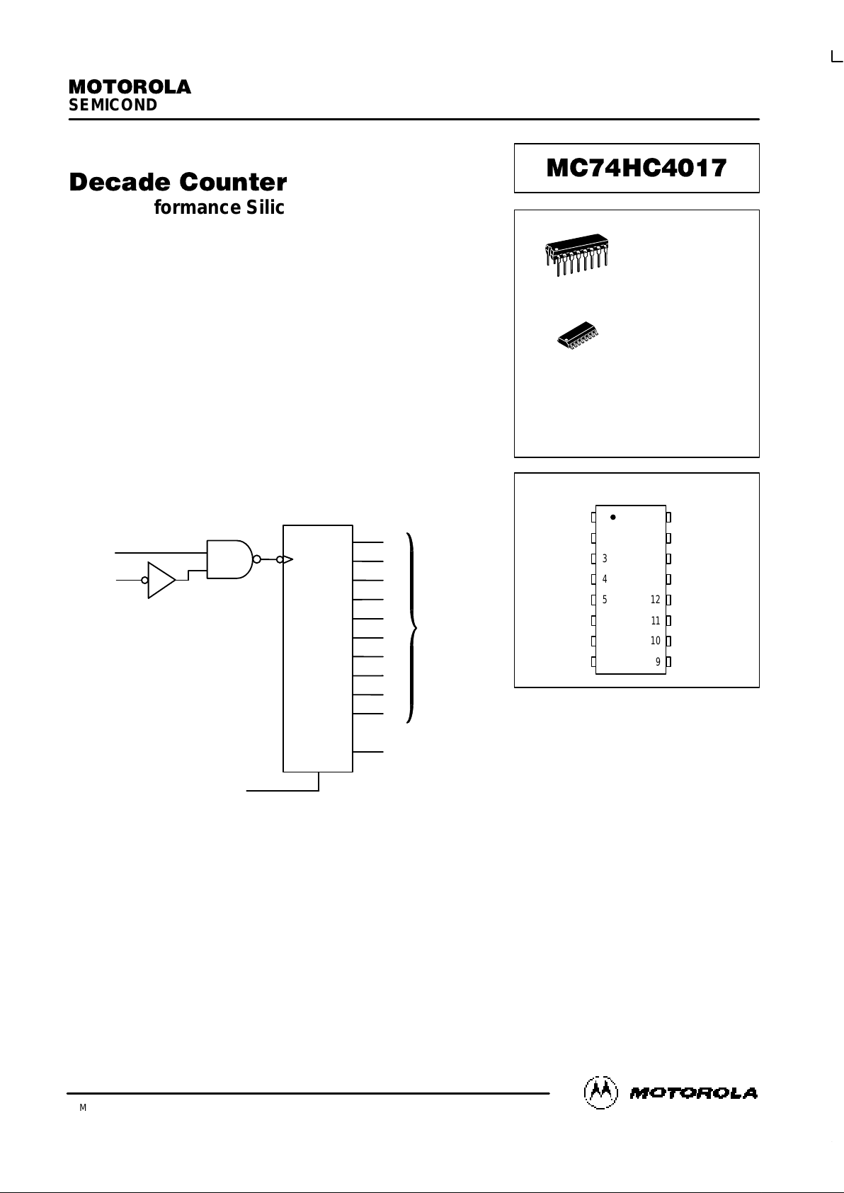
The MC74HC4017 is identical i n pinout t o the s tandard C MOS
MC14017B. The device inputs are compatible with standard CMOS outputs;
with pullup resistors, they are compatible with LSTTL outputs.
The HC4017 uses a five stage Johnson counter and decoding logic to
provide high–speed operation. This device also has an active–high, as well
as active–low clock input.
• Output Drive Capability: 10 LSTTL Loads
• Outputs Directly Interface to CMOS, NMOS, and TTL
• Operating Voltage Range: 2 to 6 V
• Low Input Current: 1 µA
• High Noise Immunity Characteristic of CMOS Devices
• In Compliance with the Requirements Defined by JEDEC Standard
No. 7A
• Chip Complexity: 176 FETs or 44 Equivalent Gates
LOGIC DIAGRAM
DECADE
OUTPUTS
PIN 16 = V
CC
PIN 8 = GND
CLOCK
ENABLE
CARRY OUT
RESET
CLOCK
Q0
Q1
Q2
Q3
Q4
Q5
Q6
Q7
Q8
Q9
15
3
2
4
7
1
5
6
9
14
13
11
12
10
PIN ASSIGNMENT
13
14
15
16
9
10
11
125
4
3
2
1
8
7
6
CARRY OUT
CLOCK ENABLE
CLOCK
RESET
V
CC
Q8
Q4
Q9
Q2
Q0
Q1
Q5
GND
Q3
Q7
Q6
D SUFFIX
SOIC PACKAGE
CASE 751B–05
N SUFFIX
PLASTIC PACKAGE
CASE 648–08
1
16
1
16
ORDERING INFORMATION
MC74HCXXXXN
MC74HCXXXXD
Plastic
SOIC
MC74HC4017
MOTOROLA High–Speed CMOS Logic Data
DL129 — Rev 6
2
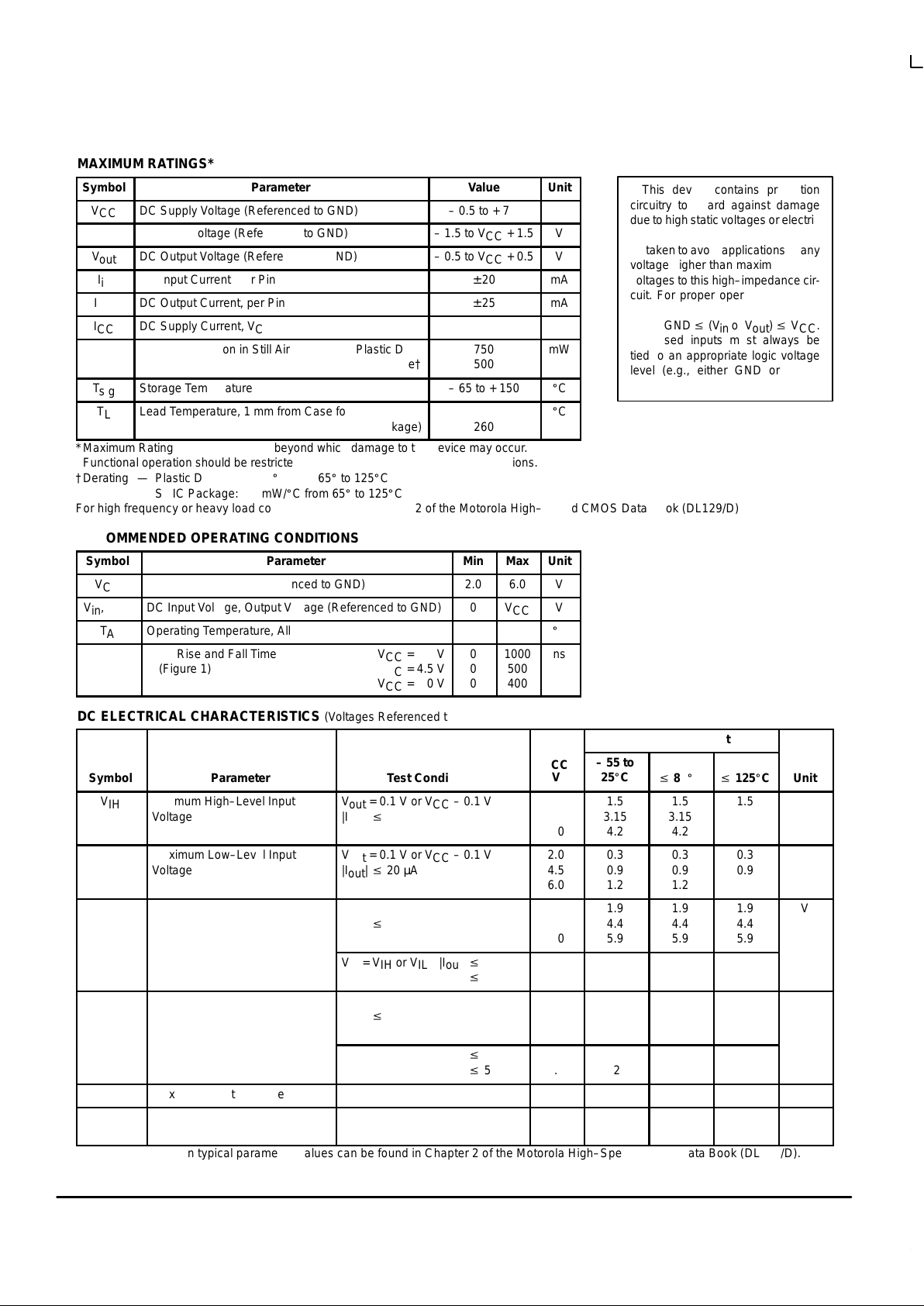
MAXIMUM RATINGS*
Symbol
Parameter
Value
Unit
V
CC
DC Supply Voltage (Referenced to GND)
– 0.5 to + 7.0
V
V
in
DC Input Voltage (Referenced to GND)
– 1.5 to VCC + 1.5
V
V
out
DC Output Voltage (Referenced to GND)
– 0.5 to VCC + 0.5
V
I
in
DC Input Current, per Pin
± 20
mA
I
out
DC Output Current, per Pin
± 25
mA
I
CC
DC Supply Current, VCC and GND Pins
± 50
mA
P
D
Power Dissipation in Still Air Plastic DIP†
SOIC Package†
750
500
mW
T
stg
Storage Temperature
– 65 to + 150
_
C
T
L
Lead Temperature, 1 mm from Case for 10 Seconds
(Plastic DIP or SOIC Package)
260
_
C
*Maximum Ratings are those values beyond which damage to the device may occur.
Functional operation should be restricted to the Recommended Operating Conditions.
†Derating — Plastic DIP: – 10 mW/_C from 65_ to 125_C
SOIC Package: – 7 mW/_C from 65_ to 125_C
For high frequency or heavy load considerations, see Chapter 2 of the Motorola High–Speed CMOS Data Book (DL129/D).
RECOMMENDED OPERATING CONDITIONS
Symbol
Parameter
Min
Max
Unit
V
CC
DC Supply Voltage (Referenced to GND)
2.0
6.0
V
Vin, V
out
DC Input Voltage, Output Voltage (Referenced to GND)
0
V
CC
V
T
A
Operating Temperature, All Package Types
– 55
+ 125
_
C
tr, t
f
Input Rise and Fall Time VCC = 2.0 V
(Figure 1) VCC = 4.5 V
VCC = 6.0 V
0
0
0
1000
500
400
ns
DC ELECTRICAL CHARACTERISTICS (Voltages Referenced to GND)
Guaranteed Limit
Symbol
Parameter
Test Conditions
V
CC
V
– 55 to
25_C
v
85_Cv 125_C
Unit
V
IH
Minimum High–Level Input
Voltage
V
out
= 0.1 V or VCC – 0.1 V
|I
out
| v 20 µA
2.0
4.5
6.0
1.5
3.15
4.2
1.5
3.15
4.2
1.5
3.15
4.2
V
V
IL
Maximum Low–Level Input
Voltage
V
out
= 0.1 V or VCC – 0.1 V
|I
out
| v 20 µA
2.0
4.5
6.0
0.3
0.9
1.2
0.3
0.9
1.2
0.3
0.9
1.2
V
V
OH
Minimum High–Level Output
Voltage
Vin = VIH or V
IL
|I
out
| v 20 µA
2.0
4.5
6.0
1.9
4.4
5.9
1.9
4.4
5.9
1.9
4.4
5.9
V
Vin = VIH or VIL|I
out
| v 4.0 mA
|I
out
| v 5.2 mA
4.5
6.0
3.98
5.48
3.84
5.34
3.70
5.20
V
OL
Maximum Low–Level Output
Voltage
Vin = VIH or V
IL
|I
out
| v 20 µA
2.0
4.5
6.0
0.1
0.1
0.1
0.1
0.1
0.1
0.1
0.1
0.1
V
Vin = VIH or VIL|I
out
| v 4.0 mA
|I
out
| v 5.2 mA
4.5
6.0
0.26
0.26
0.33
0.33
0.40
0.40
I
in
Maximum Input Leakage Current
Vin = VCC or GND
6.0
± 0.1
± 1.0
± 1.0
µA
I
CC
Maximum Quiescent Supply
Current (per Package)
Vin = VCC or GND
I
out
= 0 µA
6.0
8
80
160
µA
NOTE: Information on typical parametric values can be found in Chapter 2 of the Motorola High–Speed CMOS Data Book (DL129/D).
This device contains protection
circuitry to guard against damage
due to high static voltages or electric
fields. However, precautions must
be taken to avoid applications of any
voltage higher than maximum rated
voltages to this high–impedance circuit. For proper operation, Vin and
V
out
should be constrained to the
range GND v (Vin or V
out
) v VCC.
Unused inputs must always be
tied to an appropriate logic voltage
level (e.g., either GND or VCC).
Unused outputs must be left open.
MC74HC4017
High–Speed CMOS Logic Data
DL129 — Rev 6
3 MOTOROLA
AC ELECTRICAL CHARACTERISTICS (C
L
= 50 pF, Input tr = tf = 6 ns)
Guaranteed Limit
Symbol
Parameter
V
CC
V
– 55 to
25_C
v
85_Cv 125_C
Unit
f
max
Maximum Clock Frequency (50% Duty Cycle)
(Figures 1 and 9)
2.0
4.5
6.0
4.0
20
24
3.2
16
19
2.6
13
15
MHz
t
PLH
,
t
PHL
Maximum Propagation Delay, Clock to Q
(Figures 1 and 9)
2.0
4.5
6.0
230
46
39
290
58
49
345
69
59
ns
t
PLH
,
t
PHL
Maximum Propagation Delay, Clock to Carry Out
(Figures 2 and 9)
2.0
4.5
6.0
230
46
39
290
58
49
345
69
59
ns
t
PLH
,
t
PHL
Maximum Propagation Delay, Reset to Q
(Figures 3 and 9)
2.0
4.5
6.0
230
46
39
290
58
49
345
69
59
ns
t
PLH
Maximum Propagation Delay, Reset to Carry Out
(Figures 3 and 9)
2.0
4.5
6.0
230
46
39
290
58
49
345
69
59
ns
t
PLH
,
t
PHL
Maximum Propagation Delay, Clock Enable to Q
(Figures 4 and 9)
2.0
4.5
6.0
250
50
43
315
63
54
375
75
64
ns
t
PLH
,
t
PHL
Maximum Propagation Delay, Clock Enable to Carry Out
(Figures 5 and 9)
2.0
4.5
6.0
250
50
43
315
63
54
375
75
64
ns
t
TLH
,
t
THL
Maximum Output Transition Time, Any Output
(Figures 8 and 9)
2.0
4.5
6.0
75
15
13
95
19
16
110
22
19
ns
C
in
Maximum Input Capacitance
—
10
10
10
pF
NOTES:
1. For propagation delays with loads other than 50 pF, see Chapter 2 of the Motorola High–Speed CMOS Data Book (DL129/D).
2. Information on typical parametric values can be found in Chapter 2 of the Motorola High–Speed CMOS Data Book (DL129/D).
Typical @ 25°C, VCC = 5.0 V
C
PD
Power Dissipation Capacitance (Per Package)*
35
pF
*Used to determine the no–load dynamic power consumption: PD = CPD V
CC
2
f + ICC VCC. For load considerations, see Chapter 2 of the
Motorola High–Speed CMOS Data Book (DL129/D).
 Loading...