

MOTOROLA MC74HC1GU04DFT1 Datasheet
SEMICONDUCTOR TECHNICAL DATA
The MC74HC1GU04 is a high speed CMOS unbuffered inverter
fabricated with silicon gate CMOS technology. It achieves high speed
operation similar to equivalent LSTTL while maintaining CMOS low
power dissipation.
The internal circuit is composed of three stages, including a buffer
output which provides high noise immunity and stable output.
The MC74HC1GU04 output drive current is 1/2 compared to
MC74HC series.
• High Speed: tPD = 7ns (Typ) at VCC = 5V
• Low Power Dissipation: ICC = 1µA (Max) at TA = 25°C
• High Noise Immunity
• Balanced Propagation Delays (tpLH = tpHL)
• Output Drive Capability: 5 LSTTL
• Symmetrical Output Impedance (IOH = IOL = 2mA)
• ESD Performance: HBM > 2000V; MM > 200V
Order this document by MC74HC1GU04/D
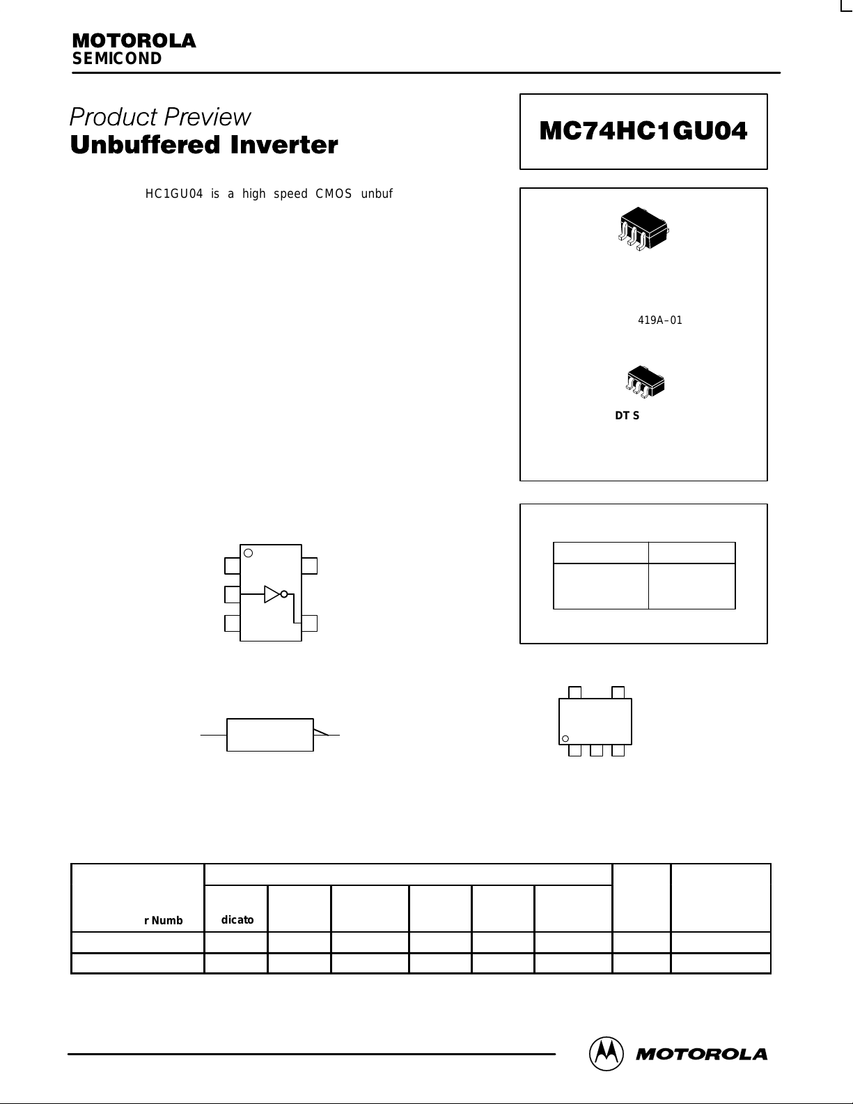
DF SUFFIX
5–LEAD SOT–353 PACKAGE
SC–88A
CASE 419A–01
DT SUFFIX
5–LEAD TSSOP PACKAGE
TSOP5
CASE TBD
FUNCTION TABLE
VCCIN C
51
A
2
YGND
43
Inputs Outputs
L
H
H
L
Figure 1. Pinout (Top View)
d
A
1
Figure 2. Logic Symbol
Y
H6
Pin 1
d = Date Code
Marking Diagram
DEVICE ORDERING INFORMATION
Device Nomenclature
Motorola
Circuit
Device Order Number
MC74HC1GU04DFT1 MC 74 HC1G U04 DF T1 SC–88A 7–Inch/3000 Unit
MC74HC1GU04DTT1 MC 74 HC1G U04 DT T1 TSOP5 7–Inch/3000 Unit
Indicator
Temp
Range
Identifier
Technology
Device
Function
Package
Suffix
Tape and
Reel Suffix
Package
Type
Tape and Reel
Size
This document contains information on a product under development. Motorola reserves the right to change or
discontinue this product without notice.
06/99
Motorola, Inc. 1999
1
REV 0.1
MC74HC1GU04
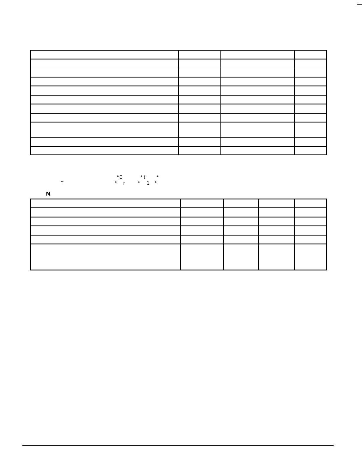
MAXIMUM RATINGS*
Characteristics Symbol Value Unit
DC Supply Voltage V
DC Input Voltage V
DC Output Voltage V
Input Diode Current I
Output Diode Current (V
DC Output Current, per Pin I
DC Supply Current, VCC and GND I
Power dissipation in still air SC–88A†
Lead temperature, 1 mm from case for 10 s T
Storage temperature T
* Maximum Ratings are those values beyond which damage to the device may occur. Exposure to these conditions or conditions beyond those
indicated may adversely affect device reliability. Functional operation under absolute–maximum–rated conditions is not implied. Functional oper-
ation should be restricted to the Recommended Operating Conditions.
†Derating — SC–88A Package: –3 mW/_C from 65_ to 125_C
— TSOP5 Package: –6 mW/_C from 65_ to 125_C
OUT
< GND; V
> VCC) I
OUT
TSOP5†
CC
IN
OUT
IK
OK
OUT
CC
P
D
L
stg
RECOMMENDED OPERATING CONDITIONS
Characteristics Symbol Min Max Unit
DC Supply Voltage V
DC Input Voltage V
DC Output Voltage V
Operating Temperature Range T
Input Rise and Fall Time VCC = 2.0V
VCC = 3.0V
VCC = 4.5V
VCC = 6.0V
CC
IN
OUT
tr , t
A
f
–0.5 to +7.0 V
–0.5 to VCC + 0.5 V
–0.5 to VCC + 0.5 V
±20 mA
±20 mA
±12.5 mA
±25 mA
200
450
260 °C
–65 to +150 °C
2.0 6.0 V
0.0 V
0.0 V
–55 +125 °C
0
0
0
0
CC
CC
1000
600
500
400
mW
ns
V
V
MOTOROLA VHC Data – Advanced CMOS Logic
2
DL203 — Rev 1
MC74HC1GU04
Î
Î
Î
Î
Î
Î
Î
Î
Î
Î
Î
Î
Î
Î
Î
Î
Î
Î
Î
Î
Î
Î
Î
Î
Î
Î
Î
Î
Î
Î
Î
Î
Î
Î
Î
Î
Î
Î
Î
Î
Î
Î
Î
Î
Î
Î
Î
Î
Î
Î
Î
Î
Î
Î
Î
Î
Î
Î
Î
Î
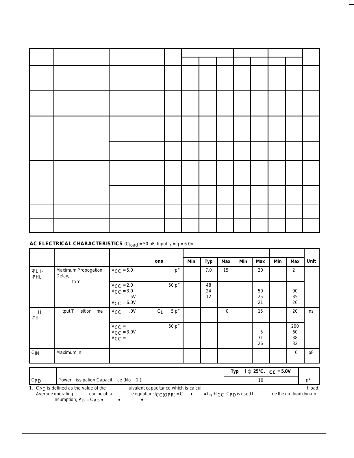
DC ELECTRICAL CHARACTERISTICS
V
CC
Symbol Parameter Test Conditions (V) Min Typ Max Min Max Min Max Unit
V
IH
Minimum High–Level
Input Voltage
2.0
3.0
4.5
6.0
V
IL
Maximum Low–Level
Input Voltage
2.0
3.0
4.5
6.0
V
V
I
I
OH
OL
IN
CC
Minimum High–Level
Output Voltage
VIN = VIH or V
IL
Maximum Low–Level
Output Voltage
VIN = VIH or V
IL
Maximum Input
Leakage Current
Maximum Quiescent
Supply Current
VIN = VIH or V
IOH = –20µA
VIN = VIH or V
IOH = –2mA
IL
IL
IOH = –2.6mA
VIN = VIH or V
IOL = 20µA
VIN = VIH or V
IOL = 2mA
IL
IL
IOL = 2.6mA
VIN = 6.0V or GND 0 to
VIN = VCC or GND 6.0 1.0 10 40 µA
2.0
3.0
4.5
6.0
4.5
6.0
2.0
3.0
4.5
6.0
4.5
6.0
6.0
TA = 25°C TA ≤ 85°C TA ≤ 125°C
1.7
2.45
3.60
4.80
1.8
2.7
4.0
5.5
4.18
5.68
1.20
2.0
3.0
4.5
5.9
4.33
5.76
0.0
0.0
0.0
0.0
0.26
0.26
0.3
0.5
0.9
0.1
0.1
0.1
0.1
1.7
2.45
3.60
4.80
0.3
0.5
0.9
1.20
1.8
2.7
4.0
5.5
4.13
5.63
0.1
0.1
0.1
0.1
0.33
0.33
±0.1 ±1.0 ±1.0 µA
1.7
2.45
3.60
4.80
0.3
0.5
0.9
1.20
1.8
2.7
4.0
5.5
4.08
5.58
0.1
0.1
0.1
0.1
0.40
0.40
V
V
V
V
V
V
AC ELECTRICAL CHARACTERISTICS (C
Symbol
t
,
PLH
t
PHL
ÎÎ
ÎÎ
ÎÎ
t
,
TLH
ÎÎ
t
THL
ÎÎ
ÎÎ
C
IN
ÎÎ
Parameter
Maximum Propogation
Delay,
ООООО
Input A to Y
ООООО
ООООО
Output Transition Time
ООООО
ООООО
ООООО
Maximum Input
Capacitance
ООООО
VCC = 5.0V CL = 15 pF
ООООООО
VCC = 2.0V CL = 50 pF
VCC = 3.0V
ООООООО
VCC = 4.5V
VCC = 6.0V
ООООООО
VCC = 5.0V CL = 15 pF
ООООООО
VCC = 2.0V CL = 50 pF
ООООООО
VCC = 3.0V
VCC = 4.5V
ООООООО
VCC = 6.0V
ОООООООÎÎÎÎ
= 50 pF, Input tr = tf = 6.0ns)
load
Test Conditions
TA = 25°C
Min
Typ
7.0
ÎÎÎ
48
24
Î
Î
12
Î
ÎÎÎ
9.0
Î
5.0
50
Î
Î
22
Î
14
Î
12
5
Max
15
Î
100
40
Î
20
17
Î
10
Î
125
Î
35
25
Î
21
10
Î
TA ≤ 85°C
Min
Max
20
ÎÎÎ
125
50
Î
Î
ÎÎÎ
Î
25
21
Î
15
155
Î
Î
Î
45
31
Î
26
10
ÎÎÎ
TA ≤ 125°C
Min
Max
25
ÎÎÎ
155
90
Î
Î
ÎÎÎ
Î
35
26
Î
20
200
Î
Î
Î
60
38
Î
32
10
ÎÎÎ
Unit
ns
ns
pF
Typical @ 25°C, VCC = 5.0V
C
PD
Power Dissipation Capacitance (Note 1.)
10
pF
1. CPD is defined as the value of the internal equivalent capacitance which is calculated from the operating current consumption without load.
Average operating current can be obtained by the equation: I
power consumption; PD = CPD V
2
fin + ICC VCC.
CC
CC(OPR
= CPD VCC fin + ICC. CPD is used to determine the no–load dynamic
)
VHC Data – Advanced CMOS Logic
DL203 — Rev 1
3 MOTOROLA
 Loading...