

SEMICONDUCTOR TECHNICAL DATA
The MC74HC1G14 is a high speed CMOS inverter with
Schmitt–Trigger input fabricated with silicon gate CMOS technology. It
achieves high speed operation similar to equivalent LSTTL while
maintaining CMOS low power dissipation.
The internal circuit is composed of three stages, including a buffer
output which provides high noise immunity and stable output.
The MC74HC1G14 output drive current is 1/2 compared to MC74HC
series.
• High Speed: tPD = 7ns (Typ) at VCC = 5V
• Low Power Dissipation: ICC = 1µA (Max) at TA = 25°C
• High Noise Immunity
• Balanced Propagation Delays (tpLH = tpHL)
• Output Drive Capability: 5 LSTTL
• Symmetrical Output Impedance (IOH = IOL = 2mA)
• ESD Performance: HBM > 2000V; MM > 200V
Order this document by MC74HC1G14/D
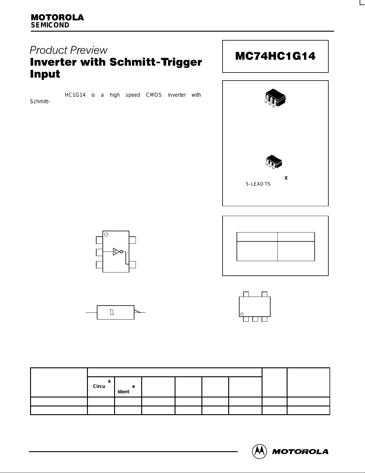
DF SUFFIX
5–LEAD SOT–353 PACKAGE
SC–88A
CASE 419A–01
DT SUFFIX
5–LEAD TSSOP PACKAGE
TSOP5
CASE TBD
FUNCTION TABLE
VCCNC
51
A
2
YGND
43
Inputs Outputs
L
H
H
L
Figure 1. Pinout (Top View)
d
A
1
Figure 2. Logic Symbol
Y
HA
Pin 1
d = Date Code
Marking Diagram
DEVICE ORDERING INFORMATION
Device Nomenclature
Motorola
Circuit
Device Order Number
MC74HC1G14DFT1 MC 74 HC1G 14 DF T1 SC–88A 7–Inch/3000 Unit
MC74HC1G14DTT1 MC 74 HC1G 14 DT T1 TSOP5 7–Inch/3000 Unit
Indicator
Temp
Range
Identifier
Technology
Device
Function
Package
Suffix
Tape and
Reel Suffix
Package
Type
Tape and Reel
Size
This document contains information on a product under development. Motorola reserves the right to change or
discontinue this product without notice.
06/99
Motorola, Inc. 1999
1
REV 0.1
MC74HC1G14
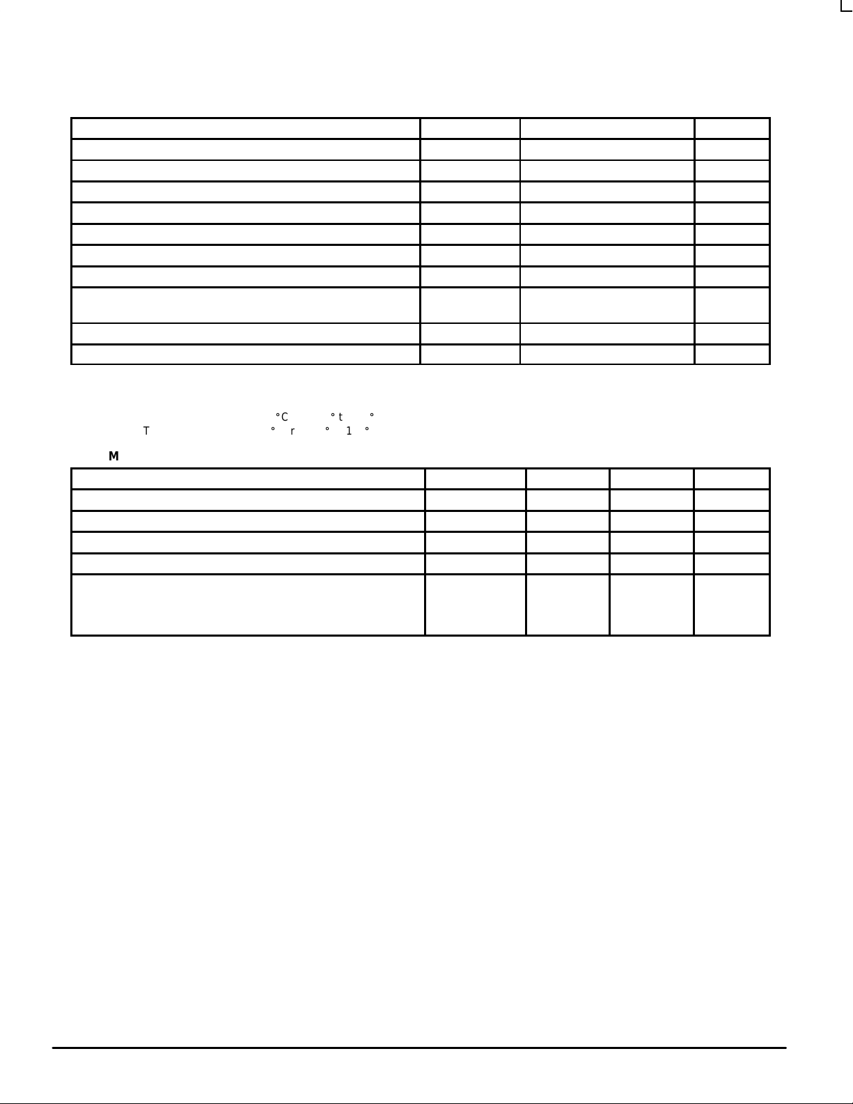
MAXIMUM RATINGS*
Characteristics Symbol Value Unit
DC Supply Voltage V
DC Input Voltage V
DC Output Voltage V
Input Diode Current I
Output Diode Current (V
DC Output Current, per Pin I
DC Supply Current, VCC and GND I
Power dissipation in still air SC–88A†
Lead temperature, 1 mm from case for 10 s T
Storage temperature T
* Maximum Ratings are those values beyond which damage to the device may occur. Exposure to these conditions or conditions beyond those
indicated may adversely affect device reliability. Functional operation under absolute–maximum–rated conditions is not implied. Functional oper-
ation should be restricted to the Recommended Operating Conditions.
†Derating — SC–88A Package: –3 mW/_C from 65_ to 125_C
— TSOP5 Package: –6 mW/_C from 65_ to 125_C
OUT
< GND; V
> VCC) I
OUT
TSOP5†
CC
IN
OUT
IK
OK
OUT
CC
P
D
L
stg
RECOMMENDED OPERATING CONDITIONS
Characteristics Symbol Min Max Unit
DC Supply Voltage V
DC Input Voltage V
DC Output Voltage V
Operating Temperature Range T
Input Rise and Fall Time VCC = 2.0V
VCC = 3.0V
VCC = 4.5V
VCC = 6.0V
CC
IN
OUT
tr , t
A
f
–0.5 to +7.0 V
–0.5 to VCC + 0.5 V
–0.5 to VCC + 0.5 V
±20 mA
±20 mA
±12.5 mA
±25 mA
200
450
260 °C
–65 to +150 °C
2.0 6.0 V
0.0 V
0.0 V
–55 +125 °C
0
0
0
0
CC
CC
1000
600
500
400
mW
ns
V
V
MOTOROLA VHC Data – Advanced CMOS Logic
2
DL203 — Rev 1
MC74HC1G14
Î
Î
Î
Î
Î
Î
Î
Î
Î
Î
Î
Î
Î
Î
Î
Î
Î
Î
Î
Î
Î
Î
Î
Î
Î
Î
Î
Î
Î
Î
Î
Î
Î
Î
Î
Î
Î
Î
Î
Î
Î
Î
Î
Î
Î
Î
Î
Î
Î
Î
Î
Î
Î
Î
DC ELECTRICAL CHARACTERISTICS
V
CC
Symbol Parameter Test Conditions (V) Min Typ Max Min Max Min Max Unit
V
T+
Positive–going
Input Threshold Voltage
V
|I
OUT
OUT
= 0.1V
| ≤ 20µA
2.0
3.0
4.5
6.0
V
T–
Negative–going
Input Threshold Voltage
V
|I
OUT
OUT
= VCC – 0.1V
| ≤ 20µA
2.0
3.0
4.5
6.0
V
V
V
I
I
H
OH
OL
IN
CC
Hysteresis Voltage V
Minimum High–Level
Output Voltage
VIN = VIH or V
IL
Maximum Low–Level
Output Voltage
VIN = VIH or V
IL
Maximum Input
Leakage Current
Maximum Quiescent
Supply Current
= 0.1V or
OUT
V
= VCC – 0.1V
OUT
|I
| ≤ 20µA
OUT
VIN = VIH or V
IOH = –20µA
IL
2.0
3.0
4.5
6.0
2.0
3.0
4.5
6.0
VIN = VIH or V
IOH = –2mA
IOH = –2.6mA
VIN = VIH or V
IOL = 20µA
IL
4.5
6.0
IL
2.0
3.0
4.5
6.0
VIN = VIH or V
IOL = 2mA
IOL = 2.6mA
IL
4.5
6.0
VIN = 6.0V or GND 0 to
6.0
VIN = VCC or GND 6.0 1.0 10 40 µA
TA = 25°C TA ≤ 85°C TA ≤ 125°C
1.00
1.50
2.30
3.00
0.30
0.50
0.90
1.20
0.20
0.25
0.40
0.50
1.9
2.9
4.4
5.9
4.18
5.68
2.0
3.0
4.5
6.0
4.31
5.80
0.0
0.0
0.0
0.0
0.17
0.18
1.50
2.15
3.15
4.20
0.90
1.40
2.00
2.60
1.25
1.65
2.25
3.00
0.1
0.1
0.1
0.1
0.26
0.26
0.95
1.45
2.25
2.95
0.30
0.50
0.90
1.20
0.20
0.25
0.40
1.20
1.9
2.9
4.4
5.9
4.13
5.63
1.60
2.20
3.15
4.20
0.95
1.45
2.05
2.65
1.25
1.65
2.25
3.00
0.1
0.1
0.1
0.1
0.33
0.33
±0.1 ±1.0 ±1.0 µA
0.90
1.40
2.20
2.90
0.30
0.50
0.90
1.20
0.20
0.25
0.40
1.20
1.9
2.9
4.4
5.9
4.08
5.58
1.60
2.20
3.15
4.20
1.00
1.50
2.10
2.70
1.25
1.65
2.25
3.00
0.1
0.1
0.1
0.1
0.40
0.40
V
V
V
V
V
V
V
AC ELECTRICAL CHARACTERISTICS (C
ÎÎ
Symbol
ÎÎ
t
,
PLH
ÎÎ
t
PHL
ÎÎ
ÎÎ
t
,
TLH
t
ÎÎ
THL
ÎÎ
ÎÎ
C
IN
ООООО
Parameter
ООООО
Maximum Propogation
ООООО
Delay,
Input A to Y
ООООО
ООООО
Output Transition Time
ООООО
ООООО
ООООО
Maximum Input
Capacitance
ООООООО
ООООООО
VCC = 5.0V CL = 15 pF
ООООООО
VCC = 2.0V CL = 50 pF
VCC = 3.0V
ООООООО
VCC = 4.5V
ООООООО
VCC = 6.0V
VCC = 5.0V CL = 15 pF
ООООООО
VCC = 2.0V CL = 50 pF
VCC = 3.0V
ООООООО
VCC = 4.5V
VCC = 6.0V
ООООООО
= 50 pF, Input tr = tf = 6.0ns)
load
Test Conditions
TA = 25°C
ООООО
MinÎTypÎMaxÎMinÎMaxÎMinÎMax
Î
ÎÎÎ
Î
Î
ÎÎÎ
Î
Î
11
48
32
Î
12
Î
9.0
4.0
50
22
Î
14
12
Î
5
21
Î
100
45
Î
20
Î
17
8.0
Î
125
35
Î
25
21
Î
10
TA ≤ 85°C
ÎÎÎ
ÎÎÎ
27
235
Î
Î
90
Î
48
Î
40
13
ÎÎÎ
145
Î
Î
45
Î
30
24
Î
10
TA ≤ 125°C
ÎÎÎ
35
ÎÎÎ
300
135
Î
Î
Î
60
Î
50
18
ÎÎÎ
200
60
Î
Î
Î
35
31
Î
10
Unit
ns
ns
pF
Typical @ 25°C, VCC = 5.0V
C
PD
Power Dissipation Capacitance (Note 1.)
10
pF
1. CPD is defined as the value of the internal equivalent capacitance which is calculated from the operating current consumption without load.
Average operating current can be obtained by the equation: I
power consumption; PD = CPD V
2
fin + ICC VCC.
CC
CC(OPR
= CPD VCC fin + ICC. CPD is used to determine the no–load dynamic
)
VHC Data – Advanced CMOS Logic
DL203 — Rev 1
3 MOTOROLA

MC74HC1G14
INPUT A
OUTPUT Y
S
TEST POINT
OUTPUT
50%
10%
90%
t
r
t
PHL
t
f
V
CC
DEVICE
UNDER
TEST
t
PLH
GND
90%
50%
10%
t
THL
t
TLH
*Includes all probe and jig capacitance
Figure 3. Switching Waveforms Figure 4. T est Circuit
OUTLINE DIMENSIONS
DF SUFFIX
5–LEAD SOT–353 P ACKAGE
SC–88A
CASE 419A–01
A
G
V
45
–B–
123
5 PL
D
MM
B0.2 (0.008)
ISSUE B
NOTES:
1. DIMENSIONING AND TOLERANCING PER ANSI
Y14.5M, 1982.
2. CONTROLLING DIMENSION: MM.
INCHES
DIMAMIN MAX MIN MAX
B 1.15 1.350.045 0.053
C 0.80 1.100.031 0.043
D 0.10 0.300.004 0.012
G 0.65 BSC0.026 BSC
H ––– 0.10–––0.004
J 0.10 0.250.004 0.010
K 0.10 0.300.004 0.012
N 0.20 REF0.008 REF
S 2.00 2.200.079 0.087
V 0.30 0.400.012 0.016
MILLIMETERS
1.80 2.200.071 0.087
CL*
H
“T1” PIN ONE TOWARDS
SPROCKET HOLE
N
C
SOT–353 (5 Pin)
DEVICE
User Direction of Feed
SOT–353
J
K
0.5 mm (min)
0.65 mm 0.65 mm
0.4 mm (min)
1.9 mm
MOTOROLA VHC Data – Advanced CMOS Logic
4
DL203 — Rev 1

PROPOSED DT SUFFIX
5–LEAD TSSOP PACKAGE
TSOP5
CASE TBD
ISSUE TBD
MC74HC1G14
0.05 (0.002)
A
L
S
1
23
45
G
H
TSOP5 (5 Pin)
DEVICE
User Direction of Feed
B
D
C
NOTES:
1. DIMENSIONING AND TOLERANCING PER ANSI
Y14.5M, 1982.
2. CONTROLLING DIMENSION: MILLIMETER.
3. MAXIMUM LEAD THICKNESS INCLUDES LEAD
FINISH THICKNESS. MINIMUM LEAD THICKNESS
IS THE MINIMUM THICKNESS OF BASE
MATERIAL.
DIM MIN MAX MIN MAX
A 0.1142 0.12202.90 3.10
B 0.0512 0.06691.30 1.70
C 0.0354 0.04330.90 1.10
D 0.0098 0.01970.25 0.50
G 0.0335 0.04130.85 1.05
M
J
K
H 0.0005 0.00400.013 0.100
J 0.0040 0.01020.10 0.26
K 0.0079 0.02360.20 0.60
L 0.0493 0.06101.25 1.55
M 0 10 0 10
____
S 0.0985 0.11812.50 3.00
INCHESMILLIMETERS
DO NOT DESIGN WITH THESE
DIMENSIONS – PRELIMINARY
0.094
2.4
0.037
0.95
0.074
1.9
0.037
0.95
0.028
0.7
VHC Data – Advanced CMOS Logic
DL203 — Rev 1
0.039
1.0
inches
mm
5 MOTOROLA

MC74HC1G14
INCLUDING DRAFT AND RADII
K
t
TOP
COVER
TAPE
B
1
FOR MACHINE REFERENCE
CONCENTRIC AROUND B
ONLY
R MIN.
K
0
SEE
NOTE 2
0
P
0
D
EMBOSSMENT
USER DIRECTION OF FEED
P
2
SEE NOTE 2A
0
B
0
P
10 PITCHES
CUMULA TIVE
TOLERANCE ON
TAPE
±
0.2 mm
±
0.008”)
(
E
F
++ +
CENTER LINES
OF CAVITY
*TOP COVER
TAPE THICKNESS (t1)
0.10 mm
(0.004”) MAX.
W
D
1
FOR COMPONENTS
2.0 mm × 1.2 mm
AND LARGER
TAPE AND COMPONENTS
BENDING RADIUS
MAXIMUM COMPONENT ROTATION
°
10
SHALL PASS AROUND RADIUS “R”
WITHOUT DAMAGE
TYPICAL
COMPONENT CAVITY
CENTER LINE
TYPICAL
COMPONENT
CENTER LINE
ALLOWABLE CAMBER TO BE 1 mm/100 mm NONACCUMULATIVE OVER 250
EMBOSSED
CARRIER
100 mm
(3.937”)
1 mm MAX
CAMBER (TOP VIEW)
1 mm
(0.039”) MAX
EMBOSSMENT
TAPE
250 mm
(9.843”)
mm
Figure 5. Carrier Tape Specifications
EMBOSSED CARRIER DIMENSIONS (See Notes 1 and 2)
Tape
Size
8 mm 4.35 mm
1. Metric Dimensions Govern–English are in parentheses for reference only.
2. A0, B0, and K0 are determined by component size. The clearance between the components and the cavity must be within 0.05 mm min to 0.50
mm max. The component cannot rotate more than 10° within the determined cavity
B
1
Max
(0.171”)
D D
1.5 +0.1/
–0.0 mm
(0.059
+0.004/
–0.0”)
1
1.0 mm
Min
(0.039”)
E F K P P
1.75
±
0.1 mm
(0.069
±
0.004”)
3.5
±
0.5 mm
(1.38
±
0.002”)
2.4 mm
(0.094”)
4.0
±
0.10 mm
(0.157
±
0.004”)
0
4.0
±
0.1 mm
(0.156
±
0.004”)
P
2
2.0
±
0.1 mm
(0.079
±
0.002”)
R T W
25 mm
(0.98”)
0.3
±
0.05 mm
(0.01
+0.0038/
–0.0002”)
8.0
±
0.3 mm
(0.315
±
0.012”)
MOTOROLA VHC Data – Advanced CMOS Logic
6
DL203 — Rev 1

1.5 mm MIN
(0.06”)
13.0 mm ±0.2 mm
±
0.008”)
(0.512”
MC74HC1G14
t MAX
20.2 mm MIN
A
(0.795”)
REEL DIMENSIONS
Tape
Size
8 mm 330 mm
FULL RADIUS
Figure 6. Reel Dimensions
A Max G t Max
(13”)
8.400 mm, +1.5 mm, –0.0
(0.33”, +0.059”, –0.00)
14.4 mm
(0.56”)
50 mm MIN
(1.969”)
G
DIRECTION OF FEED
BARCODE LABEL
Figure 7. Reel Winding Direction
HOLEPOCKET
VHC Data – Advanced CMOS Logic
DL203 — Rev 1
7 MOTOROLA

MC74HC1G14
CAVITY
TAPE
TOP T APE
TAPE TRAILER
(Connected to Reel Hub)
NO COMPONENTS
160 mm MIN
Figure 8. T ape Ends for Finished Goods
COMPONENTS
DIRECTION OF FEED
TAPE LEADER
NO COMPONENTS
400 mm MIN
Motorola reserves the right to make changes without further notice to any products herein. Motorola makes no warranty , representation or guarantee regarding
the suitability of its products for any particular purpose, nor does Motorola assume any liability arising out of the application or use of any product or circuit, and
specifically disclaims any and all liability, including without limitation consequential or incidental damages. “T ypical” parameters which may be provided in Motorola
data sheets and/or specifications can and do vary in different applications and actual performance may vary over time. All operating parameters, including “Typicals”
must be validated for each customer application by customer’s technical experts. Motorola does not convey any license under its patent rights nor the rights of
others. Motorola products are not designed, intended, or authorized for use as components in systems intended for surgical implant into the body, or other
applications intended to support or sustain life, or for any other application in which the failure of the Motorola product could create a situation where personal injury
or death may occur. Should Buyer purchase or use Motorola products for any such unintended or unauthorized application, Buyer shall indemnify and hold Motorola
and its officers, employees, subsidiaries, affiliates, and distributors harmless against all claims, costs, damages, and expenses, and reasonable attorney fees
arising out of, directly or indirectly, any claim of personal injury or death associated with such unintended or unauthorized use, even if such claim alleges that
Motorola was negligent regarding the design or manufacture of the part. Motorola and are registered trademarks of Motorola, Inc. Motorola, Inc. is an Equal
Opportunity/Affirmative Action Employer.
How to reach us:
USA/EUROPE/Locations Not Listed: Motorola Literature Distribution; JAPAN: Nippon Motorola Ltd.; SPD, Strategic Planning Office, 141,
P.O. Box 5405, Denver, Colorado 80217. 1–303–675–2140 or 1–800–441–2447 4–32–1 Nishi–Gotanda, Shinagawa–ku, Tokyo, Japan. 81–3–5487–8488
Customer Focus Center: 1–800–521–6274
Mfax: RMFAX0@email.sps.mot.com – TOUCHTONE 1–602–244–6609 ASIA/PACIFIC: Motorola Semiconductors H.K. Ltd.; 8B Tai Ping Industrial Park,
Moto rola Fax Back System – US & Canada ONLY 1–800–774–1848 51 Ting Kok Road, Tai Po, N.T., Hong Kong. 852–26629298
HOME PAGE: http://motorola.com/sps/
MOTOROLA VHC Data – Advanced CMOS Logic
– http://sps.motorola.com/mfax/
◊
8
Mfax is a trademark of Motorola, Inc.
MC74HC1G14/D
DL203 — Rev 1
 Loading...