

Motorola MC74HC194N Datasheet
SEMICONDUCTOR TECHNICAL DATA
1
REV 6
Motorola, Inc. 1995
10/95
High–Performance Silicon–Gate CMOS
The MC74HC194 is identical in pinout to the LS194 and the MC14194B
metal gate CMOS device. The device inputs are compatible with standard
CMOS outputs; with pull–up resistors, they are compatible with LSTTL
outputs.
This static shift register features parallel load, serial load (shift right and
shift left), hold, and reset modes of operation. These modes are tabulated in
the Function Table, and further e xplanation can be f ound i n the Pin
Description section.
• Output Drive Capability: 10 LSTTL Loads
• Outputs Directly Interface to CMOS, NMOS, and TTL
• Operating Voltage Range: 2 to 6 V
• Low Input Current: 1 µA
• High Noise Immunity Characteristic of CMOS Devices
• In Compliance with the Requirements Defined by JEDEC Standard
No. 7A
• Chip Complexity 164 FETs or 41 Equivalent Gates
FUNCTION TABLE
Inputs
Mode
Select
Serial
Data
Parallel Data
Outputs
Operating
Reset
S1 S0
Clock
SDSAA B C D Q
A
Q
B
Q
C
Q
D
Operating
Mode
L X X X X X X X X X L L L L Reset
H H H X X a b c d a b c d Parallel Load
H
H
LLH
H
XXHLXXXXXXX
X
HLQ
An
Q
An
Q
Bn
Q
Bn
Q
Cn
Q
Cn
Shift Right
H
H
HHL
L
HLXXXXXXXXXXQ
Bn
Q
Bn
Q
Cn
Q
Cn
Q
Dn
Q
Dn
H
L
Shift Left
H
H
H
L
X
X
L
X
X
X
L
H
X
X
X
X
X
X
X
X
X
X
X
X
X
X
X
X
X
X
No Change
No Change
No Change
Hold
H = high level (steady state) a, b, c, d = the level of steady–state input at inputs A, B, C, or D, respectively.
L = low level (steady state) QAn, QBn, QCn, QDn = the level of QA, QB, QC, or QD, respectively, before
X = don’t care the most recent transition of the clock.
= transition from low to high level.
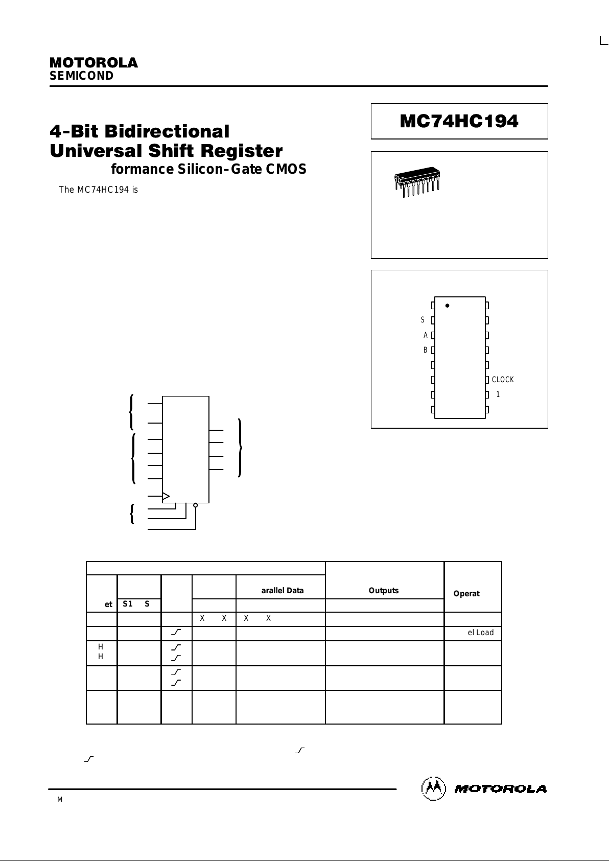
PIN ASSIGNMENT
13
14
15
16
9
10
11
125
4
3
2
1
8
7
6
Q
D
Q
C
Q
B
Q
A
V
CC
S0
S1
CLOCK
B
A
S
A
RESET
GND
D
C
S
D
N SUFFIX
PLASTIC PACKAGE
CASE 648–08
1
16
ORDERING INFORMATION
MC74HCXXXN Plastic
LOGIC DIAGRAM
15
SERIAL
DATA
INPUTS
PARALLEL
DATA
INPUTS
MODE
SELECT
S
A
S
D
A
B
C
D
CLOCK
S1
S0
RESET
PARALLEL
DATA
OUTPUTS
Q
A
Q
B
Q
C
Q
D
14
13
12
10
9
1
11
6
5
4
3
7
2
VCC = PIN 16
GND = PIN 8
MC74HC194
MOTOROLA High–Speed CMOS Logic Data
DL129 — Rev 6
2
MAXIMUM RATINGS*
Symbol
Parameter
Value
Unit
V
CC
DC Supply Voltage (Referenced to GND)
– 0.5 to + 7.0
V
V
in
DC Input Voltage (Referenced to GND)
– 1.5 to VCC + 1.5
V
V
out
DC Output Voltage (Referenced to GND)
– 0.5 to VCC + 0.5
V
I
in
DC Input Current, per Pin
± 20
mA
I
out
DC Output Current, per Pin
± 25
mA
I
CC
DC Supply Current, VCC and GND Pins
± 50
mA
P
D
Power Dissipation in Still Air Plastic DIP†
750
mW
T
stg
Storage Temperature
– 65 to + 150
_
C
T
L
Lead Temperature, 1 mm from Case for 10 Seconds
(Plastic DIP)
260
_
C
*Maximum Ratings are those values beyond which damage to the device may occur.
Functional operation should be restricted to the Recommended Operating Conditions.
†Derating — Plastic DIP: – 10 mW/_C from 65_ to 125_C
For high frequency or heavy load considerations, see Chapter 2 of the Motorola High–Speed CMOS Data Book (DL129/D).
RECOMMENDED OPERATING CONDITIONS
Symbol
Parameter
Min
Max
Unit
V
CC
DC Supply Voltage (Referenced to GND)
2.0
6.0
V
Vin, V
out
DC Input Voltage, Output Voltage (Referenced to GND)
0
V
CC
V
T
A
Operating Temperature, All Package Types
– 55
+ 125
_
C
tr, t
f
Input Rise and Fall Time VCC = 2.0 V
(Figure 1) VCC = 4.5 V
VCC = 6.0 V
0
0
0
1000
500
400
ns
DC ELECTRICAL CHARACTERISTICS (Voltages Referenced to GND)
Guaranteed Limit
Symbol
Parameter
Test Conditions
V
CC
V
– 55 to
25_C
v
85_Cv 125_C
Unit
V
IH
Minimum High–Level Input
Voltage
V
out
= 0.1 V or VCC – 0.1 V
|I
out
| v 20 µA
2.0
4.5
6.0
1.5
3.15
4.2
1.5
3.15
4.2
1.5
3.15
4.2
V
V
IL
Maximum Low–Level Input
Voltage
V
out
= 0.1 V or VCC – 0.1 V
|I
out
| v 20 µA
2.0
4.5
6.0
0.3
0.9
1.2
0.3
0.9
1.2
0.3
0.9
1.2
V
V
OH
Minimum High–Level Output
Voltage
Vin = VIH or V
IL
|I
out
| v 20 µA
2.0
4.5
6.0
1.9
4.4
5.9
1.9
4.4
5.9
1.9
4.4
5.9
V
Vin = VIH or VIL|I
out
| v 4.0 mA
|I
out
| v 5.2 mA
4.5
6.0
3.98
5.48
3.84
5.34
3.70
5.20
V
OL
Maximum Low–Level Output
Voltage
Vin = VIH or V
IL
|I
out
| v 20 µA
2.0
4.5
6.0
0.1
0.1
0.1
0.1
0.1
0.1
0.1
0.1
0.1
V
Vin = VIH or VIL|I
out
| v 4.0 mA
|I
out
| v 5.2 mA
4.5
6.0
0.26
0.26
0.33
0.33
0.40
0.40
I
in
Maximum Input Leakage Current
Vin = VCC or GND
6.0
± 0.1
± 1.0
± 1.0
µA
I
CC
Maximum Quiescent Supply
Current (per Package)
Vin = VCC or GND
I
out
= 0 µA
6.0
8
80
160
µA
NOTE: Information on typical parametric values can be found in Chapter 2 of the Motorola High–Speed CMOS Data Book (DL129/D).
This device contains protection
circuitry to guard against damage
due to high static voltages or electric
fields. However, precautions must
be taken to avoid applications of any
voltage higher than maximum rated
voltages to this high–impedance circuit. For proper operation, Vin and
V
out
should be constrained to the
range GND v (Vin or V
out
) v VCC.
Unused inputs must always be
tied to an appropriate logic voltage
level (e.g., either GND or VCC).
Unused outputs must be left open.
MC74HC194
High–Speed CMOS Logic Data
DL129 — Rev 6
3 MOTOROLA
AC ELECTRICAL CHARACTERISTICS (C
L
= 50 pF, Input tr = tf = 6 ns)
Guaranteed Limit
Symbol
Parameter
V
CC
V
– 55 to
25_C
v
85_Cv 125_C
Unit
f
max
Maximum Clock Frequency (50% Duty Cycle)
(Figures 1 and 4)
2.0
4.5
6.0
6.0
30
35
4.8
24
28
4.0
20
24
MHz
t
PLH
,
t
PHL
Maximum Propagation Delay, Clock to Q
(Figures 1 and 4)
2.0
4.5
6.0
145
29
25
180
36
31
220
44
38
ns
t
PHL
Maximum Propagation Delay, Reset to Q
(Figures 2 and 4)
2.0
4.5
6.0
150
30
26
190
38
33
225
45
38
ns
t
TLH
,
t
THL
Maximum Output Transition Time, Any Output
(Figures 1 and 4)
2.0
4.5
6.0
75
15
13
95
19
16
110
22
19
ns
C
in
Maximum Input Capacitance
—
10
10
10
pF
NOTES:
1. For propagation delays with loads other than 50 pF, see Chapter 2 of the Motorola High–Speed CMOS Data Book (DL129/D).
2. Information on typical parametric values can be found in Chapter 2 of the Motorola High–Speed CMOS Data Book (DL129/D).
Typical @ 25°C, VCC = 5.0 V
C
PD
Power Dissipation Capacitance (Per Package)*
90
pF
*Used to determine the no–load dynamic power consumption: PD = CPD V
CC
2
f + ICC VCC. For load considerations, see Chapter 2 of the
Motorola High–Speed CMOS Data Book (DL129/D).
TIMING REQUIREMENTS (Input t
r
= tf = 6 ns)
Guaranteed Limit
Symbol
Parameter
V
CC
V
– 55 to
25_C
v
85_Cv 125_C
Unit
t
su
Minimum Setup Time, Parallel Data Inputs to Clock
(Figure 3)
2.0
4.5
6.0
100
20
17
125
25
21
150
30
26
ns
t
su
Minimum Setup Time, S1 or S2 to Clock
(Figure 3)
2.0
4.5
6.0
100
20
17
125
25
21
150
30
26
ns
t
su
Minimum Setup Time, SA or SD to Clock
(Figure 3)
2.0
4.5
6.0
100
20
17
125
25
21
150
30
26
ns
t
h
Minimum Hold Time, Clock to any Input (except Reset)
(Figure 3)
2.0
4.5
6.0
3
3
3
3
3
3
3
3
3
ns
t
rec
Minimum Recovery Time, Reset Inactive to Clock
(Figure 2)
2.0
4.5
6.0
5
5
5
5
5
5
5
5
5
ns
t
w
Minimum Pulse Width, Clock
(Figure 1)
2.0
4.5
6.0
80
16
14
100
20
17
120
24
20
ns
t
w
Minimum Pulse Width, Reset
(Figure 2)
2.0
4.5
6.0
80
16
14
100
20
17
120
24
20
ns
tr, t
f
Maximum Input Rise and Fall Times
(Figure 1)
2.0
4.5
6.0
1000
500
400
1000
500
400
1000
500
400
ns
NOTE: Information on typical parametric values can be found in Chapter 2 of the Motorola High–Speed CMOS Data Book (DL129/D).
 Loading...