

MOTOROLA MC74A5-33SNTR, MC74A5-50T Datasheet
MC74
Serial Digital
Temperature Sensor
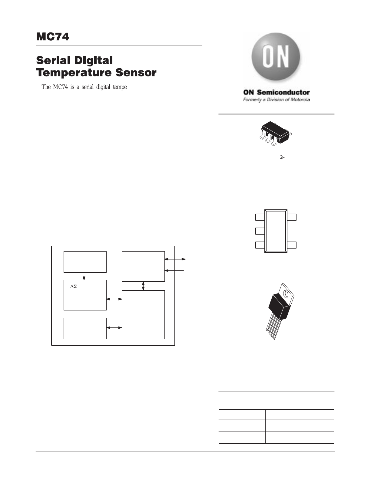
The MC74 is a serial digital temperature sensor suited for low cost
applications. Temperature data is converted from the integrated thermal
sensing element and made available as an 8–bit serial digital word.
Communication with the MC74 is accomplished via 2–wire
SMBus/I
Conversion rate is a nominal 8 samples/sec. Power consumption is
only 200 µA (5 µA Standby).
Features
• T ested Operating Temperature Range: –40°C to +125°C
• Simple Serial Port Interface
• Solid State T emperature Sensing:
• 3.3V and 5.5V Versions
Typical Applications
• Thermal Protection for Hard Disk Drives and Other PC Peripherals
• Low–Cost Thermostat Controls
• Power Supplies
2
C–compatible serial port. Temperature resolution is 1°C.
±2°C Accuracy from +25°C to +85°C
±3°C Accuracy from 0°C to +125°C
FUNCTIONAL BLOCK DIAGRAM
http://onsemi.com
SOT–23–5
SN SUFFIX
PRELIMINARY INFORMATION
GND
V
CASE TBD
PIN CONFIGURATION
(Top View)
NC
DD
1
2
3
5
4
SDA
SCL
Internal Sensor
(Diode)
DS
Modulator
Temperature
Register
Serial Port
Interface
Control
Logic
SDA
SCL
SOT–23–5*
NOTE: *SOT–23–5 is equivalent to EIAJ–SC74A
1
5
TO–220–5
T SUFFIX
CASE TBD
PRELIMINARY INFORMATION
ORDERING INFORMATION
Device Package Voltage
MC74A5–33SNTR SOT–23–5 3.3V V
DD
Semiconductor Components Industries, LLC, 1999
February , 2000 – Rev. 0
MC74A5–50T TO–220–5 5.0V V
1 Publication Order Number:
DD
MC74/D
MC74
ÁÁÁÁ
ББББББББББББББББББББББ
ÁÁÁÁ
ББББББББББББББББББББББ
ÁÁÁÁ
ББББББББББББББББББББББ
ÁÁÁÁ
ББББББББББББББББББББББ
ÁÁÁÁ
ББББББББББББББББББББББ
ÁÁÁÁ
ББББББББББББББББББББББ
ÁÁÁÁ
ББББББББББББББББББББББ
ÁÁÁÁ
ББББББББББББББББББББББ
ÁÁÁÁ
ББББББББББББББББББББББ
ÁÁÁÁ
ББББББББББББББББББББББ
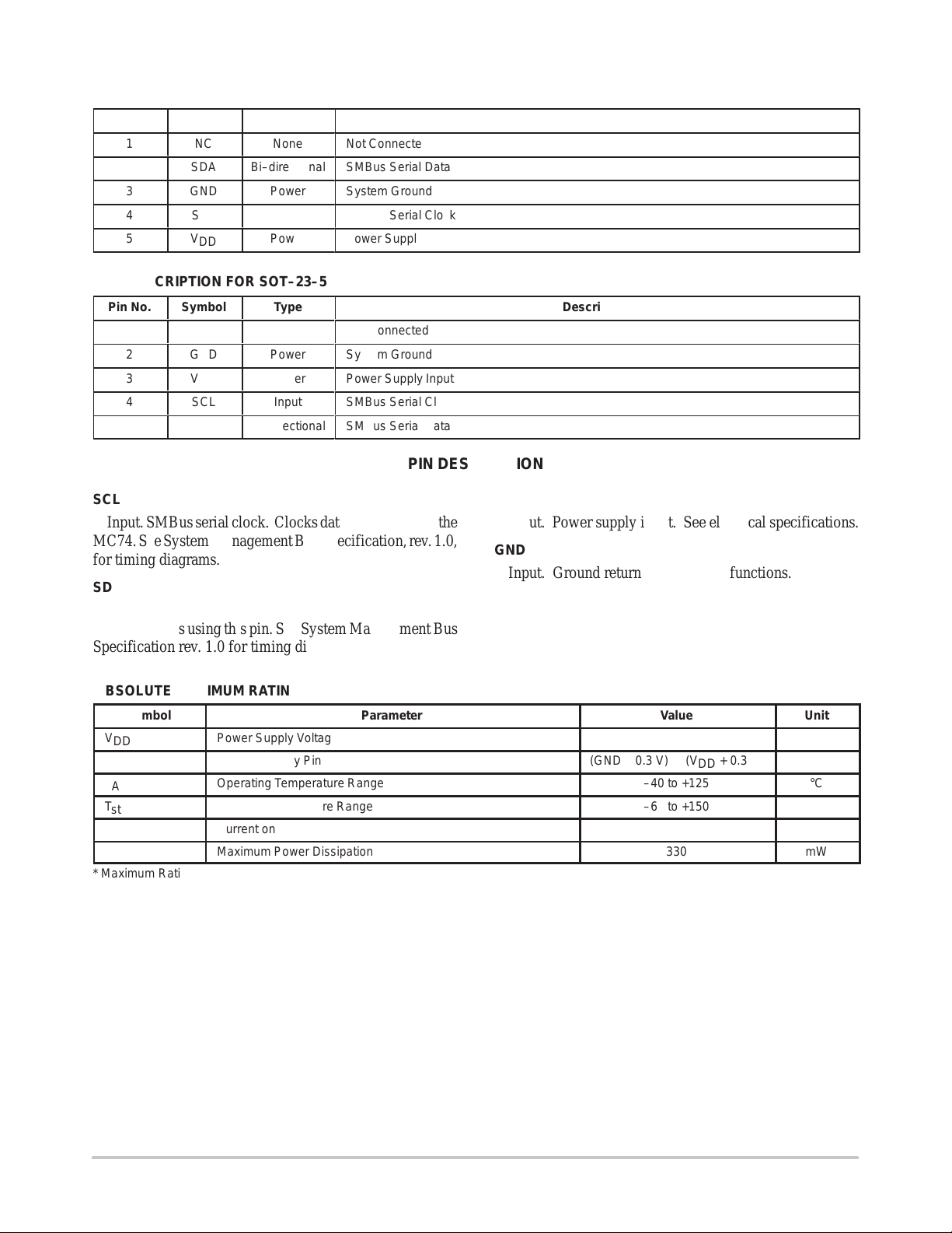
PIN DESCRIPTION FOR TO–220–5
Pin No. Symbol Type Description
1
2
3
4
5
PIN DESCRIPTION FOR SOT–23–5
Pin No. Symbol Type Description
1
2
3
4
5
NC
SDA
GND
SCL
V
DD
NC
GND
V
DD
SCL
SDA
None
Bi–directional
Power
Input
Power
None
Power
Power
Input
Bi–directional
Not Connected
SMBus Serial Data
System Ground
SMBus Serial Clock
Power Supply Input
Not Connected
System Ground
Power Supply Input
SMBus Serial Clock
SMBus Serial Data
PIN DESCRIPTION
SCL
Input. SMBus serial clock. Clocks data into and out of the
MC74. See System Management Bus Specification, rev . 1.0,
for timing diagrams.
V
DD
Input. Power supply input. See electrical specifications.
GND
Input. Ground return for all MC74 functions.
SDA
Bi–directional. Serial data is transferred on the SMBus in
both directions using this pin. See System Management Bus
Specification rev. 1.0 for timing diagrams.
ABSOLUTE MAXIMUM RATINGS*
Symbol Parameter Value Unit
V
DD
T
A
T
stg
P
D
* Maximum Ratings are those values beyond which damage to the device may occur.
Power Supply Voltage 6.0 V
Voltage on Any Pin (GND – 0.3 V) to (VDD + 0.3 V) V
Operating Temperature Range –40 to +125 °C
Storage Temperature Range –65 to +150 °C
Current on Any Pin ±50 mA
Maximum Power Dissipation 330 mW
http://onsemi.com
2
MC74
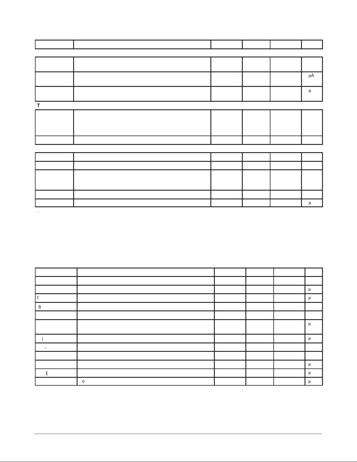
(1)
(4)
(5)
, –40°C ≤ TA ≤ 125°C, unless otherwise noted.)
1.2 — 2.2
— 200 350
— 5.0 10
–2.0
–3.0
—
4.0 8.0 — sa/sec
DD
—
—
—
—
±2.0
— — V
—
—
+2.0
+3.0
—
0.4
0.6
DD
m
m
°C
m
V
A
A
V
V
A
DC ELECTRICAL CHARACTERISTICS (VDD = 3.3 V or 5.0V
Symbol
Power Supply
V
POR
I
DD
I
DD–STANDBY
Temperature–to–Bits Converter
T
ERR
CR Conversion Rate
Serial Port Interface
V
IH
V
IL
V
OL
C
IN
I
LEAK
1. Operating current is an average value integrated over multiple conversion cycles. Transient current may exceed this specification.
2. Maximum guaranteed conversion time after Power–On RESET (POR to DATA_RDY) is 250 msec.
3. Output current should be minimized for best temperature accuracy. Power dissipation within the MC74 will cause self–heating and
temperature drift error.
4. SDA and SCL must be connected to VDD or GND.
5. VDD = 3.3V for MC74A5–33SNTR. VDD = 5.0V for MC74A5–50T . All part types of the MC74 will operate properly over the wider power supply
range of 2.7V to 5.5V . Each part type is tested and specified for rated accuracy at its nominal supply voltage. As VDD varies from the nominal
value, accuracy will degrade 1°C/V of VDD change.
Power–On Reset Threshold
(VDD Falling Edge or Rising Edge)
Operating Current
(VDD = 5.5V, Serial Port Inactive)
Standby Supply Current
(VDD = 3.3 V, Serial Port Inactive)
Temperature Accuracy MC74A
+25°C ≤ TA ≤ +85°C
0°C ≤ TA ≤ +125°C
–40°C ≤ TA ≤ 0°C
Logic Input High 0.8 x V
Logic Input Low — — 0.2 x V
SDA Output Low
IOL = 3 mA
IOL = 6 mA
Input Capacitance SDA, SCL — 5.0 — pF
I/O Leakage –1.0 0.1 1.0
(3)
(3)
Characteristic Min Typ Max Unit
(2)
SERIAL PORT AC TIMING (VDD = 3.3 V or 5.0V, –40°C ≤ (TA = TJ) ≤ 125°C; CL = 80 pF unless otherwise noted.)
Symbol
f
SMB
t
LOW
t
HIGH
t
R
t
F
t
SU(START)
t
H(START)
t
SU–DATA
t
H–DATA
t
SU(STOP)
t
IDLE
t
POR
SMBus Clock Frequency 10 — 100 kHz
Low Clock Period (10% to 10%) 4.7 — —
High Clock Period (90% to 90%) 4.0 — —
SMBus Rise Time (10% to 90%) — — 1,000 nsec
SMBus Fall Time (90% to 10%) — — 300 nsec
Start Condition Setup Time (90% SCL to 10% SDA)
(for Repeated Start Condition)
Start Condition Hold Time 4.0 — —
Data in Setup Time 1,000 — — nsec
Data in Hold Time 1,250 — — nsec
Stop Condition Setup Time 4.0 — —
Bus Free Time Prior to New Transition 4.7 — —
Power–On Reset Delay (VDD ≥ V
Characteristic Min Typ Max Unit
4.0 — —
(Rising Edge)) — 500 —
POR
m
m
m
m
m
m
m
sec
sec
sec
sec
sec
sec
sec
http://onsemi.com
3
MC74
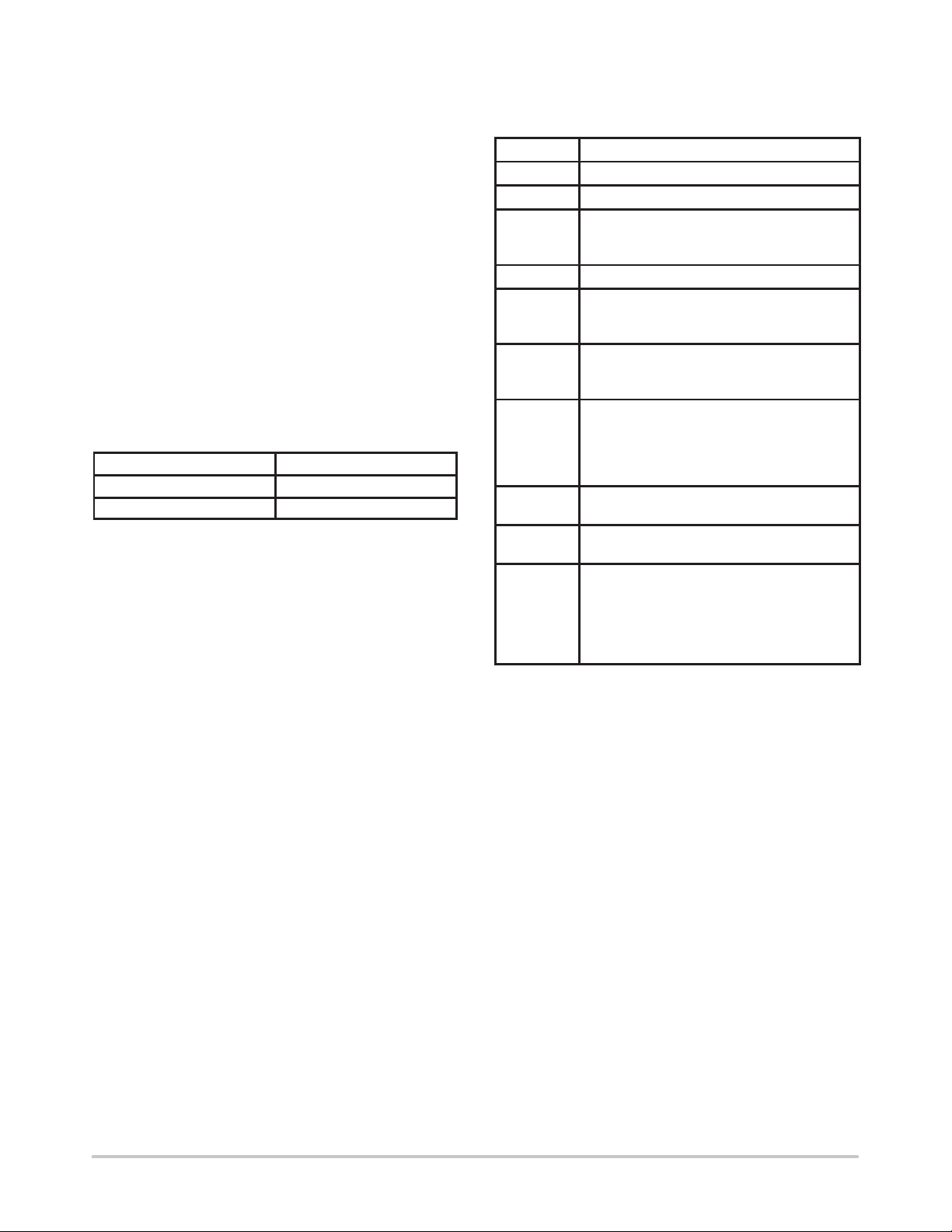
DET AILED OPERATING DESCRIPTION
The MC74 acquires and converts temperature
information from its integrated solid state sensor with a
basic accuracy of ±1°C . It stores the data in an internal
register which is read through the serial port. The system
interface is a slave SMBus. The temperature data can be
read at any time through the SMBus port. Eight SMBus
addresses are programmable for the MC74, which allows for
a multi–sensor configuration. Also, there is low–power
Standby mode where temperature acquisition is suspended.
Standby Mode
The MC74 allows the host to put it into a low power (I
DD
= 5µA, typical) Standby mode. In this mode, the A/D
converter is halted and the temperature data registers are
frozen. The SMBus port operates normally. Standby mode
is enabled by setting the SHDN bit in the CONFIG register.
The table below summarizes this operation.
Standby Mode Operation
SHDN Bit Operating Mode
0 Normal
1 Standby
SMBus Slave Address
The MC74 is internally programmed to have a default
SMBus address value of 1001 101b. Seven other addresses
are available by custom order (contact factory).
SERIAL PORT OPERATION
The Serial Clock input (SCL) and bi–directional data port
(SDA) form a 2–wire bi–directional serial port for
programming and interrogating the MC74. The following
conventions are used in this bus architecture:
MC74 Serial Bus Conventions
T erm
Transmitter The device sending data to the bus.
Receiver The device receiving data from the bus.
Master The device which controls the bus: initiating
Slave The device addressed by the master.
Start A unique condition signaling the beginning
Stop A unique condition signaling the end of a
ACK A receiver acknowledges the receipt of
Busy Communication is not possible because
NOT Busy When the bus is idle, both SDA and SCL
Data V alid The state of SDA must remain stable dur-
Explanation
transfers (START), generating the clock, and
terminating transfers (STOP).
of a transfer indicated by SDA falling (High
— Low) while SCL is high.
transfer indicated by SDA rising (Low —
High) while SCL is high.
each byte with this unique condition. The
receiver drives SDA low during SCL high
of the ACK clock–pulse. The Master provides the clock pulse for the ACK cycle.
the bus is in use.
will remain high.
ing the High period of SCL in order for a
data bit to be considered valid. SDA only
changes state while SCL is low during normal data transfers (see Start and Stop
conditions).
All transfers take place under control of a host, usually
a CPU or microcontroller, acting as the Master which
provides the clock signal for all transfers. The MC74
always operates as a Slave. The serial protocol is illustrated
in Figure 1. All data transfers have two phases; all bytes are
transferred MSB first. Accesses are initiated by a start
condition (START), followed by a device address byte and
one or more data bytes. The device address byte includes a
Read/Write selection bit. Each access must be terminated by
a Stop Condition (STOP). A convention called
Acknowledge (ACK) confirms receipt of each byte. Note
that SDA can change only during periods when SCL is LOW
(SDA changes while SCL is HIGH are reserved for Start and
Stop Conditions).
http://onsemi.com
4
 Loading...