

Motorola MC68331CFC16, MC68331VPV20, MC68331VFV20, MC68331MFV20, MC68331MPV16 Datasheet
...
Motorola reserves the right to make changes without further notice to any products herein. Motorola makes no warranty, representation or guarantee regarding the suitability
of its products for any particular purpose, nor does Motorola assume any liability arising out of the application or use of any product or circuit, and specifically disclaims any and
all liability, including without limitation consequential or incidental damages. "Typical" parameters can and do vary in different applications. All operating parameters, including
"Typicals" must be validated for each customer application by customer's technical experts. Motorola does not convey any license under its patent rights nor the rights of others.
Motorola products are not designed, intended, or authorized for use as components in systems intended for surgical implant into the body, or other applications intended to
support or sustain life, or for any other application in which the failure of the Motorola product could create a situation where personal injury or death may occur. Should Buyer
purchase or use Motorola products for any such unintended or unauthorized application, Buyer shall indemnify and hold Motorola and its officers, employees, subsidiaries,
affiliates, and distributors harmless against all claims, costs, damages, and expenses, and reasonable attorney fees arising out of, directly or indirectly, any claim of personal
injury or death associated with such unintended or unauthorized use, even if such claim alleges that Motorola was negligent regarding the design or manufacture of the part.
MOTOROLA and ! are registered trademarks of Motorola, Inc. Motorola, Inc. is an Equal Opportunity/Affirmative Action Employer.
© MOTOROLA, INC. 1996
MC68331
User’s Manual


MC68331 MOTOROLA
USER’S MANUAL iii
Paragraph Title Page
SECTION 1INTRODUCTION
SECTION 2NOMENCLATURE
2.1 Symbols and Operators ..................................................................................2-1
2.2 CPU32 Registers ............................................................................................2-2
2.3 Pin and Signal Mnemonics .............................................................................2-3
2.4 Register Mnemonics .......................................................................................2-5
2.5 Conventions ...................................................................................................2-6
SECTION 3OVERVIEW
3.1 MCU Features ................................................................................................3-1
3.1.1 System Integration Module (SIM) ...........................................................3-1
3.1.2 Central Processing Unit (CPU32) ...........................................................3-1
3.1.3 Queued Serial Module (QSM) ................................................................3-1
3.1.4 General-Purpose Timer (GPT) ...............................................................3-2
3.2 System Block Diagram and Pin Assignment Diagrams ..................................3-2
3.3 Pin Descriptions .............................................................................................3-5
3.4 Signal Descriptions .........................................................................................3-7
3.5 Intermodule Bus ...........................................................................................3-10
3.6 System Memory Map ...................................................................................3-10
3.6.1 Internal Register Map ...........................................................................3-10
3.6.2 Address Space Maps ...........................................................................3-10
3.7 System Reset ...............................................................................................3-16
3.7.1 SIM Reset Mode Selection ...................................................................3-16
3.7.2 MCU Module Pin Function During Reset .............................................3-17
SECTION 4 SYSTEM INTEGRATION MODULE
4.1 General ...........................................................................................................4-1
4.2 System Configuration and Protection .............................................................4-2
4.2.1 Module Mapping .....................................................................................4-3
4.2.2 Interrupt Arbitration .................................................................................4-3
4.2.3 Show Internal Cycles ..............................................................................4-4
4.2.4 Factory Test Mode .................................................................................4-4
4.2.5 Register Access .....................................................................................4-4
4.2.6 Reset Status ...........................................................................................4-4
4.2.7 Bus Monitor ............................................................................................4-4
4.2.8 Halt Monitor ............................................................................................4-5
4.2.9 Spurious Interrupt Monitor ......................................................................4-5
4.2.10 Software Watchdog ................................................................................4-5
TABLE OF CONTENTS

MOTOROLA MC68331
iv USER’S MANUAL
TABLE OF CONTENTS
(Continued)
Paragraph Title Page
4.2.11 Periodic Interrupt Timer ..........................................................................4-7
4.2.12 Low-Power STOP Operation ..................................................................4-8
4.2.13 Freeze Operation ...................................................................................4-9
4.3 System Clock .................................................................................................4-9
4.3.1 Clock Sources ......................................................................................4-10
4.3.2 Clock Synthesizer Operation ................................................................4-10
4.3.3 External Bus Clock ...............................................................................4-15
4.3.4 Low-Power Operation ...........................................................................4-15
4.3.5 Loss of Reference Signal .....................................................................4-16
4.4 External Bus Interface ..................................................................................4-17
4.4.1 Bus Signals ..........................................................................................4-18
4.4.1.1 Address Bus ................................................................................. 4-18
4.4.1.2 Address Strobe ............................................................................ 4-18
4.4.1.3 Data Bus ...................................................................................... 4-18
4.4.1.4 Data Strobe .................................................................................. 4-18
4.4.1.5 Read/Write Signal ........................................................................ 4-18
4.4.1.6 Size Signals ................................................................................. 4-18
4.4.1.7 Function Codes ............................................................................ 4-19
4.4.1.8 Data and Size Acknowledge Signals ...........................................4-19
4.4.1.9 Bus Error Signal ...........................................................................4-19
4.4.1.10 Halt Signal .................................................................................... 4-20
4.4.1.11 Autovector Signal ......................................................................... 4-20
4.4.2 Dynamic Bus Sizing .............................................................................4-20
4.4.3 Operand Alignment ..............................................................................4-21
4.4.4 Misaligned Operands ...........................................................................4-21
4.4.5 Operand Transfer Cases ......................................................................4-22
4.5 Bus Operation ..............................................................................................4-22
4.5.1 Synchronization to CLKOUT ................................................................4-23
4.5.2 Regular Bus Cycles ..............................................................................4-23
4.5.2.1 Read Cycle ................................................................................... 4-24
4.5.2.2 Write Cycle ................................................................................... 4-25
4.5.3 Fast Termination Cycles .......................................................................4-25
4.5.4 CPU Space Cycles ...............................................................................4-26
4.5.4.1 Breakpoint Acknowledge Cycle .................................................... 4-27
4.5.4.2 LPSTOP Broadcast Cycle ............................................................ 4-30
4.5.5 Bus Exception Control Cycles ..............................................................4-30
4.5.5.1 Bus Errors .................................................................................... 4-32
4.5.5.2 Double Bus Faults ........................................................................ 4-32
4.5.5.3 Retry Operation ............................................................................ 4-33
4.5.5.4 Halt Operation .............................................................................. 4-33
4.5.6 External Bus Arbitration ........................................................................4-34

MC68331 MOTOROLA
USER’S MANUAL v
TABLE OF CONTENTS
(Continued)
Paragraph Title Page
4.5.6.1 Slave (Factory Test) Mode Arbitration ......................................... 4-35
4.5.6.2 Show Cycles ................................................................................ 4-35
4.6 Reset ............................................................................................................ 4-36
4.6.1 Reset Exception Processing ................................................................4-36
4.6.2 Reset Control Logic ..............................................................................4-37
4.6.3 Reset Mode Selection ..........................................................................4-37
4.6.3.1 Data Bus Mode Selection ............................................................. 4-38
4.6.3.2 Clock Mode Selection .................................................................. 4-40
4.6.3.3 Breakpoint Mode Selection .......................................................... 4-40
4.6.4 MCU Module Pin Function During Reset .............................................4-40
4.6.5 Pin State During Reset .........................................................................4-41
4.6.5.1 Reset States of SIM Pins ............................................................. 4-41
4.6.5.2 Reset States of Pins Assigned to Other MCU Modules ............... 4-42
4.6.6 Reset Timing ........................................................................................4-42
4.6.7 Power-On Reset ...................................................................................4-43
4.6.8 Reset Processing Summary .................................................................4-44
4.6.9 Reset Status Register ..........................................................................4-45
4.7 Interrupts ......................................................................................................4-45
4.7.1 Interrupt Exception Processing ............................................................4-45
4.7.2 Interrupt Priority and Recognition .........................................................4-45
4.7.3 Interrupt Acknowledge and Arbitration .................................................4-46
4.7.4 Interrupt Processing Summary .............................................................4-47
4.7.5 Interrupt Acknowledge Bus Cycles .......................................................4-48
4.8 Chip Selects .................................................................................................4-48
4.8.1 Chip-Select Registers ...........................................................................4-50
4.8.1.1 Chip-Select Pin Assignment Registers ........................................ 4-51
4.8.1.2 Chip-Select Base Address Registers ...........................................4-52
4.8.1.3 Chip-Select Option Registers ....................................................... 4-52
4.8.1.4 PORTC Data Register .................................................................. 4-54
4.8.2 Chip-Select Operation ..........................................................................4-54
4.8.3 Using Chip-Select Signals for Interrupt Acknowledge ..........................4-54
4.8.4 Chip-Select Reset Operation ................................................................4-55
4.9 Parallel Input/Output Ports ...........................................................................4-57
4.9.1 Pin Assignment Registers ....................................................................4-57
4.9.2 Data Direction Registers ......................................................................4-57
4.9.3 Data Registers ......................................................................................4-57
4.10 Factory Test .................................................................................................4-57
SECTION 5 CENTRAL PROCESSING UNIT
5.1 General ...........................................................................................................5-1
5.2 CPU32 Registers ............................................................................................5-2

MOTOROLA MC68331
vi USER’S MANUAL
TABLE OF CONTENTS
(Continued)
Paragraph Title Page
5.2.1 Data Registers ........................................................................................5-4
5.2.2 Address Registers ..................................................................................5-5
5.2.3 Program Counter ....................................................................................5-6
5.2.4 Control Registers ....................................................................................5-6
5.2.4.1 Status Register ............................................................................... 5-6
5.2.4.2 Alternate Function Code Registers ................................................ 5-6
5.2.5 Vector Base Register (VBR) ...................................................................5-7
5.3 Memory Organization .....................................................................................5-7
5.4 Virtual Memory ...............................................................................................5-9
5.5 Addressing Modes ..........................................................................................5-9
5.6 Processing States ..........................................................................................5-9
5.7 Privilege Levels ............................................................................................5-10
5.8 Instructions ................................................................................................... 5-10
5.8.1 M68000 Family Compatibility ...............................................................5-14
5.8.2 Special Control Instructions ..................................................................5-14
5.8.2.1 Low Power Stop (LPSTOP) ......................................................... 5-14
5.8.2.2 Table Lookup and Interpolate (TBL) ............................................ 5-14
5.9 Exception Processing ...................................................................................5-14
5.9.1 Exception Vectors ................................................................................5-15
5.9.2 Types of Exceptions .............................................................................5-16
5.9.3 Exception Processing Sequence ..........................................................5-17
5.10 Development Support ...................................................................................5-17
5.10.1 M68000 Family Development Support .................................................5-17
5.10.2 Background Debugging Mode ..............................................................5-18
5.10.2.1 Enabling BDM .............................................................................. 5-19
5.10.2.2 BDM Sources ...............................................................................5-19
5.10.2.3 Entering BDM ............................................................................... 5-20
5.10.2.4 BDM Commands .......................................................................... 5-21
5.10.2.5 Background Mode Registers ........................................................ 5-21
5.10.2.6 Returning from BDM .................................................................... 5-22
5.10.2.7 Serial Interface ............................................................................. 5-22
5.10.2.8 Recommended BDM Connection ................................................. 5-24
5.10.3 Deterministic Opcode Tracking ............................................................5-24
5.10.4 On-Chip Breakpoint Hardware .............................................................5-25
5.11 Loop Mode Instruction Execution .................................................................5-25
SECTION 6QUEUED SERIAL MODULE
6.1 General ...........................................................................................................6-1
6.2 QSM Registers and Address Map ..................................................................6-2
6.2.1 QSM Global Registers ............................................................................6-2
6.2.1.1 Low-Power Stop Operation ............................................................ 6-2

MC68331 MOTOROLA
USER’S MANUAL vii
TABLE OF CONTENTS
(Continued)
Paragraph Title Page
6.2.1.2 Freeze Operation ........................................................................... 6-3
6.2.1.3 QSM Interrupts ............................................................................... 6-3
6.2.2 QSM Pin Control Registers ....................................................................6-4
6.3 Queued Serial Peripheral Interface ................................................................6-5
6.3.1 QSPI Registers .......................................................................................6-6
6.3.1.1 Control Registers ........................................................................... 6-7
6.3.1.2 Status Register ............................................................................... 6-7
6.3.2 QSPI RAM ..............................................................................................6-7
6.3.2.1 Receive RAM ................................................................................. 6-8
6.3.2.2 Transmit RAM ................................................................................ 6-8
6.3.2.3 Command RAM .............................................................................. 6-8
6.3.3 QSPI Pins ...............................................................................................6-8
6.3.4 QSPI Operation ......................................................................................6-9
6.3.5 QSPI Operating Modes ........................................................................6-10
6.3.5.1 Master Mode ................................................................................ 6-17
6.3.5.2 Master Wraparound Mode ........................................................... 6-19
6.3.5.3 Slave Mode .................................................................................. 6-20
6.3.5.4 Slave Wraparound Mode ............................................................. 6-21
6.3.6 Peripheral Chip Selects ........................................................................6-21
6.4 Serial Communication Interface ...................................................................6-22
6.4.1 SCI Registers .......................................................................................6-22
6.4.1.1 Control Registers ......................................................................... 6-22
6.4.1.2 Status Register ............................................................................. 6-25
6.4.1.3 Data Register ............................................................................... 6-25
6.4.2 SCI Pins ...............................................................................................6-25
6.4.3 SCI Operation .......................................................................................6-25
6.4.3.1 Definition of Terms .......................................................................6-26
6.4.3.2 Serial Formats .............................................................................. 6-26
6.4.3.3 Baud Clock ................................................................................... 6-26
6.4.3.4 Parity Checking ............................................................................ 6-27
6.4.3.5 Transmitter Operation .................................................................. 6-27
6.4.3.6 Receiver Operation ...................................................................... 6-29
6.4.3.7 Idle-Line Detection ....................................................................... 6-29
6.4.3.8 Receiver Wakeup ......................................................................... 6-30
6.4.3.9 Internal Loop ................................................................................ 6-31
6.5 QSM Initialization .........................................................................................6-31
SECTION 7GENERAL-PURPOSE TIMER
7.1 General ...........................................................................................................7-1
7.2 GPT Registers and Address Map ...................................................................7-2
7.3 Special Modes of Operation ...........................................................................7-3

MOTOROLA MC68331
viii USER’S MANUAL
TABLE OF CONTENTS
(Continued)
Paragraph Title Page
7.3.1 Low-Power Stop Mode ...........................................................................7-3
7.3.2 Freeze Mode ..........................................................................................7-3
7.3.3 Single-Step Mode ...................................................................................7-3
7.3.4 Test Mode ..............................................................................................7-4
7.4 Polled and Interrupt-Driven Operation ............................................................7-4
7.4.1 Polled Operation .....................................................................................7-4
7.4.2 GPT Interrupts ........................................................................................7-5
7.5 Pin Descriptions .............................................................................................7-6
7.5.1 Input Capture Pins (IC[1:3]) ....................................................................7-6
7.5.2 Input Capture/Output Compare Pin (IC4/OC5) ......................................7-6
7.5.3 Output Compare Pins (OC[1:4]) .............................................................7-6
7.5.4 Pulse Accumulator Input Pin (PAI) .........................................................7-7
7.5.5 Pulse-Width Modulation (PWMA, PWMB) ..............................................7-7
7.5.6 Auxiliary Timer Clock Input (PCLK) ........................................................7-7
7.6 General-Purpose I/O ......................................................................................7-7
7.7 Prescaler ........................................................................................................7-8
7.8 Capture/Compare Unit ...................................................................................7-9
7.8.1 Timer Counter ......................................................................................7-11
7.8.2 Input Capture Functions .......................................................................7-11
7.8.3 Output Compare Functions ..................................................................7-12
7.8.3.1 Output Compare 1 ........................................................................ 7-13
7.8.3.2 Forced Output Compare .............................................................. 7-13
7.9 Input Capture 4/Output Compare 5 ..............................................................7-13
7.10 Pulse Accumulator .......................................................................................7-14
7.11 Pulse-Width Modulation Unit ........................................................................7-15
7.11.1 PWM Counter .......................................................................................7-16
7.11.2 PWM Function ......................................................................................7-17
APPENDIX A ELECTRICAL CHARACTERISTICS
APPENDIX B MECHANICAL DATA AND ORDERING INFORMATION
APPENDIX CDEVELOPMENT SUPPORT
C.1 M68MMDS1632 Modular Development System ...................................... C-1
C.2 M68MEVB1632 Modular Evaluation Board .............................................. C-2
APPENDIX D REGISTER SUMMARY
D.1 Central Processing Unit ............................................................................ D-1
D.1.1 CPU32 Register Model ..................................................................... D-2
D.1.2 — Status Register ............................................................................ D-3

MC68331 MOTOROLA
USER’S MANUAL ix
TABLE OF CONTENTS
(Continued)
Paragraph Title Page
D.2 General-Purpose Timer ............................................................................ D-4
D.2.1 GPTMCR — GPT Module Configuration Register............................ D-4
D.2.2 GPTMTR — GPT Module Test Register (Reserved)........................ D-5
D.2.3 ICR — GPT Interrupt Configuration Register.................................... D-5
D.2.4 DDRGP — Port GP Data Direction Register.....................................D-6
D.2.5 OC1M— OC1 Action Mask Register................................................. D-6
D.2.6 TCNT — Timer Counter Register .....................................................D-6
D.2.7 PACTL — Pulse Accumulator Control Register................................ D-7
D.2.8 TIC[1:3] — Input Capture Registers 1–3 .......................................... D-8
D.2.9 TOC[1:4] — Output Compare Registers 1–4 ...................................D-8
D.2.10 TI4/O5 — Input Capture 4/Output Compare 5 Register.................... D-8
D.2.11 TCTL1/TCTL2 — Timer Control Registers 1 and 2...........................D-8
D.2.12 TMSK1/TMSK2 — Timer Interrupt Mask Registers 1 and 2 .............D-9
D.2.13 TFLG1/TFLG2 — Timer Interrupt Flag Registers 1 and 2.............. D-10
D.2.14 CFORC — Compare Force Register............................................... D-10
D.2.15 PWMA/PWMB — PWM Registers A/B ........................................... D-12
D.2.16 PWMCNT — PWM Count Register ...............................................D-12
D.2.17 PWMBUFA — PWM Buffer Register A .......................................... D-12
D.2.18 PRESCL — GPT Prescaler ............................................................D-12
D.3 System Integration Module ..................................................................... D-13
D.3.1 SIMCR — Module Configuration Register ...................................... D-14
D.3.2 SIMTR — System Integration Test Register................................... D-15
D.3.3 SYNCR — Clock Synthesizer Control Register .............................D-15
D.3.4 RSR — Reset Status Register ....................................................... D-16
D.3.5 SIMTRE — System Integration Test Register (ECLK).................... D-17
D.3.6 PORTE0/PORTE1 — Port E Data Register.................................... D-17
D.3.7 DDRE — Port E Data Direction Register ........................................D-17
D.3.8 PEPAR — Port E Pin Assignment Register.................................... D-17
D.3.9 PORTF0/PORTF1 — Port F Data Register..................................... D-18
D.3.10 DDRF — Port F Data Direction Register.........................................D-18
D.3.11 PFPAR — Port F Pin Assignment Register..................................... D-18
D.3.12 SYPCR — System Protection Control Register.............................. D-19
D.3.13 PICR — Periodic Interrupt Control Register....................................D-20
D.3.14 PITR — Periodic Interrupt Timer Register ...................................... D-20
D.3.15 SWSR — Software Service Register ..............................................D-21
D.3.16 TSTMSRA — Master Shift Register A............................................. D-21
D.3.17 TSTMSRB — Master Shift Register B............................................. D-21
D.3.18 TSTSC — Test Module Shift Count ................................................D-21
D.3.19 TSTRC — Test Module Repetition Count....................................... D-21
D.3.20 CREG — Test Submodule Control Register .................................. D-21
D.3.21 DREG — Distributed Register.........................................................D-21

MOTOROLA MC68331
x USER’S MANUAL
TABLE OF CONTENTS
(Continued)
Paragraph Title Page
D.3.22 PORTC — Port C Data Register..................................................... D-21
D.3.23 CSPAR0 — Chip Select Pin Assignment Register 0....................... D-21
D.3.24 CSPAR1 — Chip Select Pin Assignment Register 1....................... D-22
D.3.25 CSBARBT — Chip Select Base Address Register Boot ROM .......D-23
D.3.26 CSORBT — Chip Select Option Register Boot ROM...................... D-23
D.4 Queued Serial Module ............................................................................ D-25
D.4.1 QSMCR — QSM Configuration Register ........................................D-25
D.4.2 QTEST — QSM Test Register........................................................ D-26
D.4.3 QILR — QSM Interrupt Level Register............................................D-26
D.4.4 SCCR0 — SCI Control Register 0 .................................................. D-27
D.4.5 SCCR1 — SCI Control Register 1................................................... D-27
D.4.6 SCSR — SCI Status Register......................................................... D-29
D.4.7 SCDR — SCI Data Register............................................................ D-30
D.4.8 PORTQS — Port QS Data Register ...............................................D-30
D.4.9 PQSPAR — PORT QS Pin Assignment Register........................... D-30
D.4.10 SPCR0 — QSPI Control Register 0................................................ D-32
D.4.11 SPCR1 — QSPI Control Register 1 ............................................... D-33
D.4.12 SPCR2 — QSPI Control Register 2 ............................................... D-34
D.4.13 SPCR3 — QSPI Control Register 3 ............................................... D-34
D.4.14 RR[0:F] — Receive Data RAM........................................................D-35
D.4.15 TR[0:F] — Transmit Data RAM ...................................................... D-35
D.4.16 CR[0:F] — Command RAM.............................................................D-36

MC68331 MOTOROLA
USER’S MANUAL xi
Figure Title Page
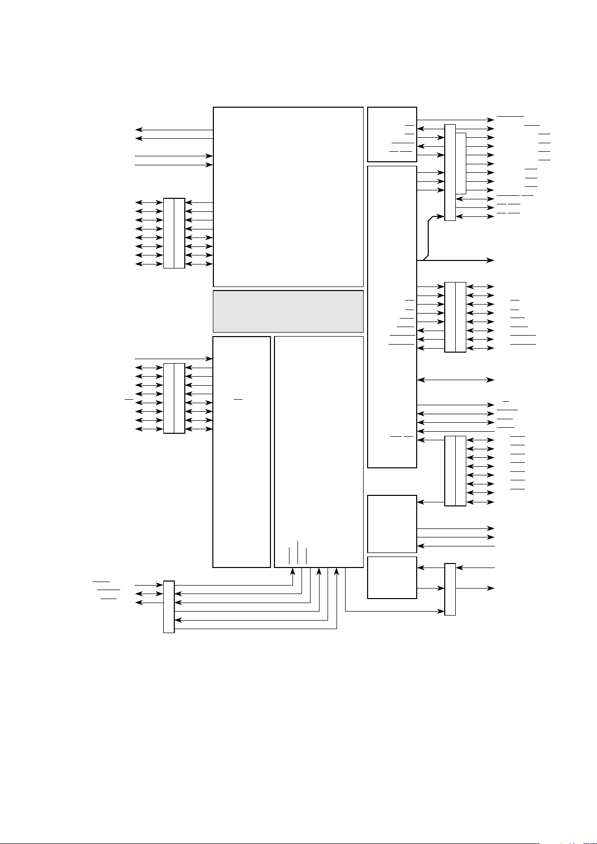
3-1 MCU Block Diagram........................................................................................ 3-3
3-2 Pin Assignments for 132-Pin Package............................................................ 3-4
3-3 Pin Assignments for 144-Pin Package............................................................ 3-5
3-4 Internal Register Memory Map...................................................................... 3-11
3-5 Overall Memory Map..................................................................................... 3-12
3-6 Separate Supervisor and User Space Map................................................... 3-13
3-7 Supervisor Space (Separate Program/Data Space) Map............................. 3-14
3-8 User Space (Separate Program/Data Space) Map....................................... 3-15
4-1 System Integration Module Block Diagram.....................................................4-2
4-2 System Configuration and Protection.............................................................. 4-3
4-3 Periodic Interrupt Timer and Software Watchdog Timer.................................4-7
4-4 System Clock Block Diagram.......................................................................... 4-9
4-5 System Clock Oscillator Circuit.....................................................................4-10
4-6 System Clock Filter Networks....................................................................... 4-11
4-7 MCU Basic System....................................................................................... 4-17
4-8 Operand Byte Order...................................................................................... 4-21
4-9 Word Read Cycle Flowchart..........................................................................4-24
4-10 Write Cycle Flowchart................................................................................... 4-25
4-11 CPU Space Address Encoding..................................................................... 4-27
4-12 Breakpoint Operation Flowchart.................................................................... 4-29
4-13 LPSTOP Interrupt Mask Level.......................................................................4-30
4-14 Bus Arbitration Flowchart for Single Request................................................4-35
4-15 Data Bus Mode Select Conditioning..............................................................4-39
4-16 Power-On Reset............................................................................................ 4-44
4-17 Basic MCU System....................................................................................... 4-49
4-18 Chip-Select Circuit Block Diagram................................................................4-50
4-19 CPU Space Encoding for Interrupt Acknowledge..........................................4-55
5-1 CPU32 Block Diagram.................................................................................... 5-2
5-2 User Programming Model............................................................................... 5-3
5-3 Supervisor Programming Model Supplement..................................................5-3
5-4 Data Organization in Data Registers............................................................... 5-5
5-5 Address Organization in Address Registers....................................................5-5
5-6 Memory Operand Addressing......................................................................... 5-8
5-7 Common In-Circuit Emulator Diagram.......................................................... 5-18
5-8 Bus State Analyzer Configuration................................................................. 5-19
5-9 Debug Serial I/O Block Diagram................................................................... 5-23
5-10 BDM Serial Data Word.................................................................................. 5-24
5-11 BDM Connector Pinout..................................................................................5-24
5-12 Loop Mode Instruction Sequence..................................................................5-25
6-1 QSM Block Diagram........................................................................................ 6-1
6-2 QSPI Block Diagram....................................................................................... 6-6
LIST OF ILLUSTRATIONS

MOTOROLA MC68331
xii USER’S MANUAL
(Continued)
Figure Title Page
LIST OF ILLUSTRATIONS
6-3 QSPI RAM....................................................................................................... 6-7
6-4 Flowchart of QSPI Initialization Operation.....................................................6-11
6-5 Flowchart of QSPI Master Operation (Part 1)............................................... 6-12
6-5 Flowchart of QSPI Master Operation (Part 2)............................................... 6-13
6-5 Flowchart of QSPI Master Operation (Part 3)............................................... 6-14
6-6 Flowchart of QSPI Slave Operation (Part 1)................................................. 6-15
6-6 Flowchart of QSPI Slave Operation (Part 2)................................................. 6-16
6-7 SCI Transmitter Block Diagram..................................................................... 6-23
6-8 SCI Receiver Block Diagram......................................................................... 6-24
7-1 GPT Block Diagram.........................................................................................7-2
7-2 Prescaler Block Diagram................................................................................. 7-9
7-3 Capture/Compare Unit Block Diagram.......................................................... 7-10
7-4 Input Capture Timing Example...................................................................... 7-12
7-5 Pulse Accumulator Block Diagram................................................................ 7-15
7-6 PWM Block Diagram.....................................................................................7-16
A-1 CLKOUT Output Timing Diagram..................................................................A-12
A-2 External Clock Input Timing Diagram............................................................A-12
A-3 ECLK Output Timing Diagram.......................................................................A-12
A-4 Read Cycle Timing Diagram .........................................................................A-13
A-5 Write Cycle Timing Diagram..........................................................................A-14
A-6 Fast Termination Read Cycle Timing Diagram .............................................A-15
A-7 Fast Termination Write Cycle Timing Diagram..............................................A-16
A-8 Bus Arbitration Timing Diagram — Active Bus Case ....................................A-17
A-9 Bus Arbitration Timing Diagram — Idle Bus Case ........................................A-18
A-10 Show Cycle Timing Diagram.........................................................................A-18
A-11 Chip Select Timing Diagram..........................................................................A-19
A-12 Reset and Mode Select Timing Diagram.......................................................A-19
A-13 Background Debugging Mode Timing Diagram—Serial Communication......A-21
A-14 Background Debugging Mode Timing Diagram —Freeze Assertion.............A-21
A-15 ECLK Timing Diagram...................................................................................A-23
A-16 QSPI Timing — Master, CPHA = 0 ...............................................................A-25
A-17 QSPI Timing — Master, CPHA = 1 ...............................................................A-25
A-18 QSPI Timing — Slave, CPHA = 0 .................................................................A-26
A-19 QSPI Timing — Slave, CPHA = 1 .................................................................A-26
B-1 132-Pin Plastic Surface Mount Package Pin Assignments.............................B-2
B-2 144-Pin Plastic Surface Mount Package Pin Assignments.............................B-3
D-1 User Programming Model...............................................................................D-2
D-2 Supervisor Programming Model Supplement..................................................D-2

MC68331 MOTOROLA
USER’S MANUAL xiii
Table Title Page
3-1 MCU Driver Types .......................................................................................... 3-6
3-2 MCU Pin Characteristics ................................................................................3-6
3-3 MCU Power Connections ............................................................................... 3-7
3-4 Signal Characteristics .....................................................................................3-7
3-5 Signal Function ...............................................................................................3-8
3-6 SIM Reset Mode Selection ........................................................................... 3-16
3-7 Module Pin Functions ................................................................................... 3-17
4-1 Show Cycle Enable Bits ................................................................................. 4-4
4-2 Bus Monitor Period ......................................................................................... 4-5
4-3 MODCLK Pin and SWP Bit During Reset ...................................................... 4-6
4-4 Software Watchdog Ratio ...............................................................................4-6
4-5 MODCLK Pin and PTP Bit at Reset ............................................................... 4-7
4-6 Periodic Interrupt Priority ................................................................................ 4-8
4-7 Clock Control Multipliers ...............................................................................4-12
4-8 System Frequencies from 32.768-kHz Reference ....................................... 4-14
4-9 Clock Control ................................................................................................ 4-16
4-10 Size Signal Encoding ................................................................................... 4-19
4-11 Address Space Encoding ............................................................................. 4-19
4-12 Effect of DSACK Signals .............................................................................. 4-20
4-13 Operand Transfer Cases .............................................................................. 4-22
4-14 DSACK, BERR, and HALT Assertion Results .............................................4-31
4-15 Reset Source Summary ...............................................................................4-37
4-16 Reset Mode Selection .................................................................................. 4-38
4-17 Module Pin Functions ................................................................................... 4-41
4-18 SIM Pin Reset States ................................................................................... 4-42
4-19 Chip-Select Pin Functions ............................................................................ 4-51
4-20 Pin Assignment Field Encoding ....................................................................4-51
4-21 Block Size Encoding .....................................................................................4-52
4-22 Option Register Function Summary .............................................................4-53
4-23 Chip Select Base and Option Register Reset Values .................................. 4-56
4-24 CSBOOT Base and Option Register Reset Values .....................................4-57
5-1 Instruction Set Summary .............................................................................. 5-11
5-2 Exception Vector Assignments .....................................................................5-16
5-3 BDM Source Summary .................................................................................5-19
5-4 Polling the BDM Entry Source ...................................................................... 5-20
5-5 Background Mode Command Summary ......................................................5-21
5-6 CPU Generated Message Encoding ............................................................ 5-24
6-1 QSM Pin Function .......................................................................................... 6-4
6-2 QSPI Pin Function .......................................................................................... 6-9
6-3 BITS Encoding ............................................................................................. 6-18
6-4 SCI Pin Function .......................................................................................... 6-25
LIST OF TABLES

MOTOROLA MC68331
xiv USER’S MANUAL
(Continued)
Table Title Page
LIST OF TABLES
6-5 Serial Frame Formats ...................................................................................6-26
6-6 Effect of Parity Checking on Data Size .........................................................6-27
7-1 GPT Status Flags ............................................................................................7-4
7-2 GPT Interrupt Sources ....................................................................................7-5
7-3 PWM Frequency Ranges Using 16.78-MHz/20.97-MHz System Clocks ......7-17
A-1 Maximum Ratings ..........................................................................................A-1
A-2 Typical Ratings, 16.78 MHz Operation ..........................................................A-2
A-2 Typical Ratings, 20.97 MHz Operation .........................................................A-2
A-3 Thermal Characteristics .................................................................................A-3
A-4 16.78 MHz Clock Control Timing ...................................................................A-3
A-4 20.97 MHz Clock Control Timing ...................................................................A-4
A-5 16.78 MHz DC Characteristics .......................................................................A-5
A-5 20.97 MHz DC Characteristics .......................................................................A-6
A-6 16.78 MHz AC Timing .................................................................................... A-8
A-6 20.97 MHz AC Timing .................................................................................... A-9
A-7 Background Debugging Mode Timing .......................................................... A-20
A-8 16.78 MHz ECLK Bus Timing ......................................................................A-22
A-8 20.97 MHz ECLK Bus Timing ......................................................................A-22
A-9 QSPI Timing .................................................................................................A-24
B-1 MCU Ordering Information ............................................................................. B-4
B-2 Quantity Order Suffix ......................................................................................B-4
C-1 MC68331 Development Tools ........................................................................C-1
D-1 Module Address Map .....................................................................................D-1
D-2 GPT Address Map ..........................................................................................D-4
D-3 SIM Address Map .........................................................................................D-13
D-4 Port E Pin Assignments ...............................................................................D-18
D-5 Port F Pin Assignments ................................................................................D-19
D-6 Software Watchdog Ratio ............................................................................D-19
D-7 Bus Monitor Period .......................................................................................D-20
D-8 CSPAR0 Pin Assignments ...........................................................................D-22
D-9 CSPAR1 Pin Assignments ...........................................................................D-22
D-10 CSPAR0 and CSPAR1 Pin Assignment Field Encoding ..............................D-22
D-11 Block Size Encoding ....................................................................................D-23
D-12 Option Register Function Summary .............................................................D-24
D-13 QSM Address Map .......................................................................................D-25
D-14 PQSPAR Pin Assignments ..........................................................................D-31
D-15 Effect of DDRQS on PORTQS Pins .............................................................D-31
D-16 Effect of DDRQS on QSM Pin Function .......................................................D-32
D-17 MC68331 Module Address Map ...................................................................D-37
D-18 Register Bit and Field Mnemonics ...............................................................D-40

MC68331
INTRODUCTION
MOTOROLA
USER’S MANUAL 1-1
1
SECTION 1INTRODUCTION
The MC68331, a highly-integrated 32-bit microcontroller, combines high-performance
data manipulation capabilities with powerful peripheral subsystems. The MCU is built
up from standard modules that interface through a common intermodule bus (IMB).
Standardization facilitates rapid development of devices tailored for specific applications.
The MCU incorporates a 32-bit CPU (CPU32), a system integration module (SIM), a
general-purpose timer (GPT), and a queued serial module (QSM).
The MCU can either synthesize an internal clock signal from an external reference or
use an external clock input directly. Operation with a 32.768-kHz reference frequency
is standard. Because MCU operation is fully static, register and memory contents are
not affected by a loss of clock.
High-density complementary metal-oxide semiconductor (HCMOS) architecture
makes the basic power consumption of the MCU low. Power consumption can be minimized by stopping the system clock. The CPU32 instruction set includes a low-power
stop (LPSTOP) command that efficiently implements this capability.
Documentation for the Modular Microcontroller Family follows the modular construction of the devices in the product line. Each microcontroller has a comprehensive user's manual that provides sufficient information for normal operation of the device. The
user's manual is supplemented by module reference manuals that provide detailed information about module operation and applications. Refer to Motorola publication
Ad-
vanced Microcontroller Unit (AMCU) Literature
(BR1116/D) for a complete listing of
documentation.

MOTOROLA
INTRODUCTION
MC68331
1-2 USER’S MANUAL
1

MC68331
NOMENCLATURE
MOTOROLA
USER’S MANUAL 2-1
2
SECTION 2NOMENCLATURE
The following nomenclature is used throughout the manual. Nomenclature used only
in certain sections, such as register bit mnemonics, is defined in those sections.
2.1 Symbols and Operators
+
— Addition
−
— Subtraction or negation (two's complement)
∗
— Multiplication
/
— Division
>
— Greater
<
— Less
=
— Equal
≥
— Equal or greater
≤
— Equal or less
≠
— Not equal
• — AND
✛
— Inclusive OR (OR)
⊕
— Exclusive OR (EOR)
NOT
— Complementation
:
— Concatenation
⇒
— Transferred
⇔
— Exchanged
±
— Sign bit; also used to show tolerance
« — Sign extension
% — Binary value
$ — Hexadecimal value

MOTOROLA
NOMENCLATURE
MC68331
2-2 USER’S MANUAL
2
2.2 CPU32 Registers
A6–A0 — Address registers (index registers)
A7 (SSP) — Supervisor Stack Pointer
A7 (USP) — User Stack Pointer
CCR — Condition code register (user portion of SR)
D7–D0 — Data Registers (index registers)
DFC — Alternate function code register
PC — Program counter
SFC — Alternate function code register
SR — Status register
VBR — Vector base register
X — Extend indicator
N — Negative indicator
Z — Zero indicator
V — Two's complement overflow indicator
C — Carry/borrow indicator

MC68331
NOMENCLATURE
MOTOROLA
USER’S MANUAL 2-3
2
2.3 Pin and Signal Mnemonics
ADDR[23:0] — Address Bus
AS
— Address Strobe
AVEC
— Autovector
BERR
— Bus Error
BG
— Bus Grant
BGACK
— Bus Grant Acknowledge
BKPT
— Breakpoint
BR
— Bus Request
CLKOUT — System Clock
CS[10:0]
— Chip Selects
CSBOOT
— Boot ROM Chip Select
DATA[15:0] — Data Bus
DS
— Data Strobe
DSACK[1:0]
— Data and Size Acknowledge
DSCLK — Development Serial Clock
DSI — Development Serial Input
DSO — Development Serial Output
EXTAL — External Crystal Oscillator Connection
FC[2:0] — Function Codes
FREEZE — Freeze
HALT
— Halt
IC[4:1] — Input Capture
IFETCH
— Instruction Fetch
IPIPE
— Instruction Pipeline
IRQ[7:1]
— Interrupt Request
MISO — Master In Slave Out
MODCLK — Clock Mode Select
MOSI — Master Out Slave In
OC[5:1] — Output Compare
PAI — Pulse Accumulator Input
PC[6:0] — SIM I/O Port C
PCLK — Pulse Accumulator Clock
PCS[3:0] — Peripheral Chip Selects
PE[7:0] — SIM I/O Port E
PF[7:0] — SIM I/O Port F
PGP[7:0] — GPT I/O Port
PQS[7:0] — QSM I/O Port
PWMA, PWMB — Pulse Width Modulator Output
QUOT — Quotient Out

MOTOROLA
NOMENCLATURE
MC68331
2-4 USER’S MANUAL
2
R/W — Read/Write
RESET
— Reset
RMC
— Read-Modify-Write Cycle
RXD — SCI Receive Data
SCK — QSPI Serial Clock
SIZ[1:0] — Size
SS
— Slave Select
TSC — Three-State Control
TXD — SCI Transmit Data
XFC — External Filter Capacitor
XTAL — External Crystal Oscillator Connection

MC68331
NOMENCLATURE
MOTOROLA
USER’S MANUAL 2-5
2
2.4 Register Mnemonics
CFORC — GPT Compare Force Register
CREG — Test Control Register C
CR[0:F] — QSM Command RAM
CSBARBT — Chip-Select Base Address Register Boot ROM
CSBAR[0:10] — Chip-Select Base Address Registers [0:10]
CSORBT — Chip-Select Option Register Boot ROM
CSOR[0:10] — Chip-Select Option Register [0:10]
CSPAR[0:1] — Chip-Select Pin Assignment Registers [0:1]
DDRE — Port E Data Direction Register
DDRF — Port F Data Direction Register
DDRGP — Port GP Data Direction Register
DDRQS — Port QS Data Direction Register
DREG — SIM Test Module Distributed Register
GPTMCR — GPT Module Configuration Register
ICR — GPT Interrupt Configuration Register
OC1D — Output Compare 1 Action Data Register
OC1M — Output Compare 1 Action Mask Register
PACNT — Pulse Accumulator Counter
PACTL — Pulse Accumulator Control Register
PEPAR — Port E Pin Assignment Register
PFPAR — Port F Pin Assignment Register
PICR — Periodic Interrupt Control Register
PITR — Periodic Interrupt Timer Register
PORTC — Port C Data Register
PORTE — Port E Data Register
PORTF — Port F Data Register
PORTGP — Port GP Data Register
PORTQS — Port QS Data Register
PQSPAR — Port QS Pin Assignment Register
PRESCL — GPT Prescaler Register
PWMA — PWM Control Register A
PWMB — PWM Control Register B
PWMBUFA — PWM Buffer Register A
PWMBUFB — PWM Buffer Register B
PWMC — PWM Control Register C
PWMCNT — PWM Counter
QILR — QSM Interrupt Level Register
QIVR — QSM Interrupt Vector Register
QSMCR — QSM Configuration Register

MOTOROLA
NOMENCLATURE
MC68331
2-6 USER’S MANUAL
2
2.5 Conventions
Logic level one is the voltage that corresponds to a Boolean true (1) state.
Logic level zero is the voltage that corresponds to a Boolean false (0) state.
Set refers specifically to establishing logic level one on a bit or bits.
Clear refers specifically to establishing logic level zero on a bit or bits.
Asserted means that a signal is in active logic state. An active low signal changes
from logic level one to logic level zero when asserted, and an active high signal changes from logic level zero to logic level one.
Negated means that an asserted signal changes logic state. An active low signal
changes from logic level zero to logic level one when negated, and an active high signal changes from logic level one to logic level zero.
QTEST — QSM Test Register
RR[0:F] — QSM Receive Data RAM
RSR — Reset Status Register
SCCR[0:1] — SCI Control Registers [0:1]
SCDR — SCI Data Register
SCSR — SCI Status Register
SIMCR — SIM Module Configuration Register
SIMTR — System Integration Test Register
SIMTRE — System Integration Test Register (ECLK)
SPCR[0:3] — QSPI Control Registers [0:3]
SPSR — QSPI Status Register
SWSR — Software Watchdog Service Register
SYNCR — Clock Synthesizer Control Register
SYPCR — System Protection Control Register
TCNT — Timer Counter Register
TCTL[1:2] — Timer Control Registers [1:2]
TFLG[1:2] — Timer Interrupt Flag Registers [1:2]
TI4/O5 — Timer Input Capture 4/Output Compare 5 Register
TIC[1:3] — Timer Input Capture Registers [1:3]
TMSK[1:2] — Timer Interrupt Mask Register [1:2]
TOC[1:4] — Timer Output Compare Registers [1:4]
TR[0:F] — QSM Transmit Data RAM
TSTMSRA — Test Module Master Shift Register A
TSTMSRB — Test Module Master Shift Register B
TSTRC — Test Module Repetition Count Register
TSTSC — Test Module Shift Count Register

MC68331 NOMENCLATURE MOTOROLA
USER’S MANUAL 2-7
2
A specific mnemonic within a range is referred to by mnemonic and number. A15 is
bit 15 of accumulator A; ADDR7 is line 7 of the address bus; CSOR0 is chip-select option register 0. A range of mnemonics is referred to by mnemonic and the numbers
that define the range. AM[35:30] are bits 35 to 30 of accumulator M; CSOR[0:5] are
the first six option registers.
Parentheses are used to indicate the content of a register or memory location, rather
than the register or memory location itself. (A) is the content of accumulator A. (M : M
+ 1) is the content of the word at address M.
LSB means least significant bit or bits. MSB means most significant bit or bits. Refer-
ences to low and high bytes are spelled out.
LSW means least significant word or words. MSW means most significant word or
words.
ADDR is the address bus. ADDR[7:0] are the eight LSB of the address bus.
DATA is the data bus. DATA[15:8] are the eight MSB of the data bus.

MOTOROLA NOMENCLATURE MC68331
2-8 USER’S MANUAL
2

MC68331 OVERVIEW MOTOROLA
USER’S MANUAL 3-1
3
SECTION 3OVERVIEW
This section contains information about the entire modular microcontroller. It lists the
features of each module, shows device functional divisions and pin assignments, summarizes signal and pin functions, discusses the intermodule bus, and provides system
memory maps. Timing and electrical specifications for the entire microcontroller and
for individual modules are provided in APPENDIX A ELECTRICAL CHARACTERIS-
TICS. Comprehensive module register descriptions and memory maps are provided
in APPENDIX D REGISTER SUMMARY.
3.1 MCU Features
The following paragraphs highlight capabilities of each of the microcontroller modules.
Each module is discussed separately in a subsequent section of this user's manual.
3.1.1 System Integration Module (SIM)
• External Bus Support
• Programmable Chip-Select Outputs
• System Protection Logic
• Watchdog Timer, Clock Monitor, and Bus Monitor
• System Protection Logic
• PLL System Clock for Low Power Operation
• Background Debugging Mode
3.1.2 Central Processing Unit (CPU32)
• Instruction Set Supports Controller Applications
• 32-Bit Architecture
• Virtual Memory Implementation
• Loop Mode of Instruction Execution
• Table Lookup and Interpolate Instruction
• Improved Exception Handling for Controller Applications
• Trace on Change of Flow
• Hardware Breakpoint Signal, Background Mode
• Fully Static Operation
3.1.3 Queued Serial Module (QSM)
• Serial Communication Interface (SCI), Enhanced Universal Asynchronous Receiver Transmitter (UART) with Modulus Baud Rate, Parity
• Queued Serial Peripheral Interface (SPI), High Speed Bidirectional Interface, 80Byte RAM, Up to 16 Automatic Transfers
• Dual Function I/O Ports
• Continuous Cycling, 8 to 16 Bits per Transfer

MOTOROLA OVERVIEW MC68331
3-2 USER’S MANUAL
3
3.1.4 General-Purpose Timer (GPT)
• Two 16-Bit Free-Running Counters With One Nine-Stage Prescaler
• Three Input Capture Channels
• Four Output Compare Channels
• One Input Capture/Output Compare Channel
• One Pulse Accumulator/Event Counter Input
• Two Pulse-Width Modulation Outputs
• Optional External Clock Input
3.2 System Block Diagram and Pin Assignment Diagrams
Figure 3-1 is a functional diagram of the MCU. Although diagram blocks represent the
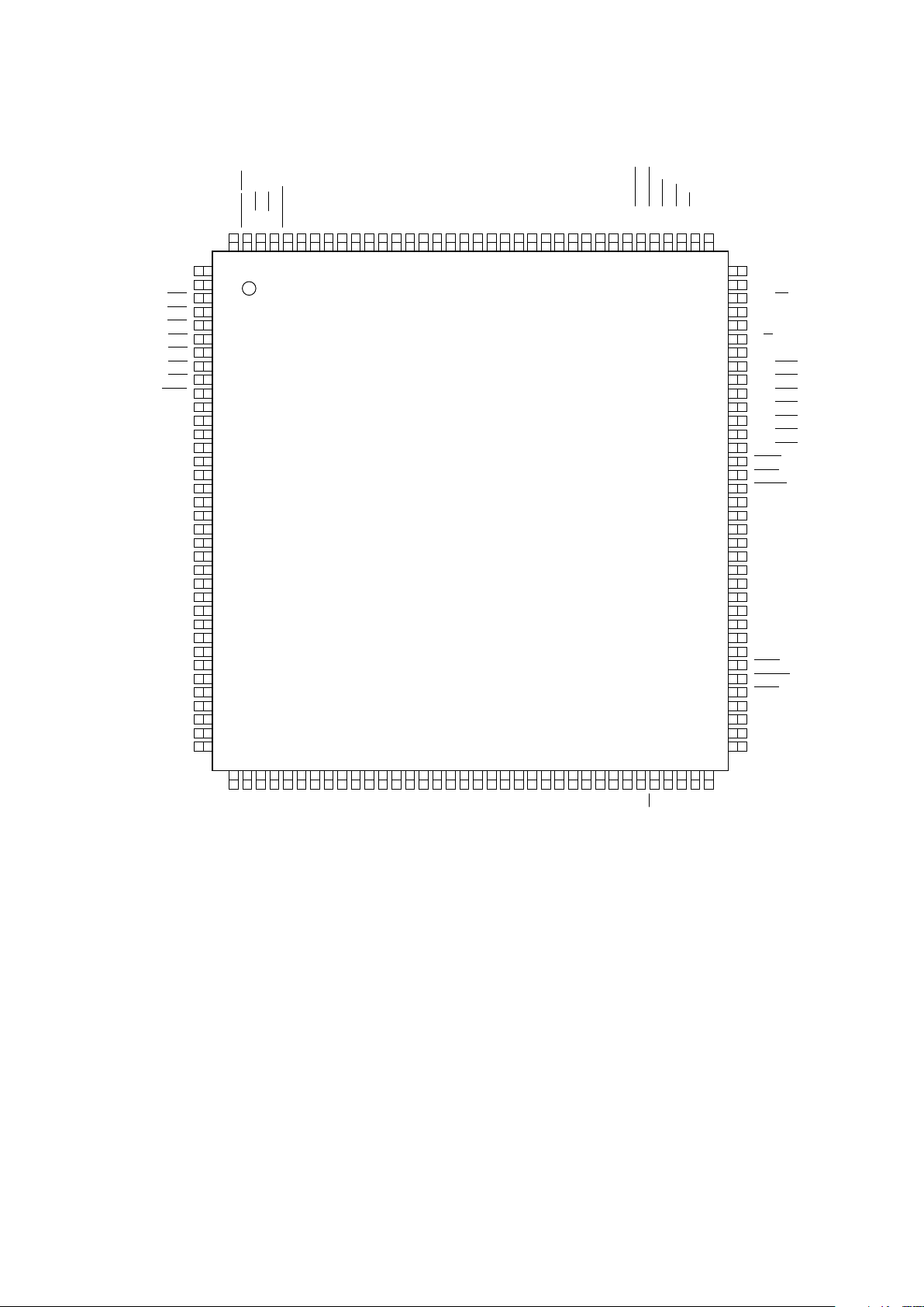
relative size of the physical modules, there is not a one-to-one correspondence between location and size of blocks in the diagram and location and size of integratedcircuit modules. Figure 3-2 shows the pin assignments of the 132-pin plastic surfacemount package. Figure 3-3 shows the pin assignments of the 144-pin plastic surfacemount package. Refer to APPENDIX B MECHANICAL DATA AND ORDERING IN-
FORMATION for package dimensions. All pin functions and signal names are shown
in this drawing. Refer to subsequent paragraphs in this section for pin and signal descriptions.
MC68331 OVERVIEW MOTOROLA
USER’S MANUAL 3-3
3
Figure 3-1 MCU Block Diagram
331 BLOCK
PQS5/PCS2
PQS7/TXD
PQS4/PCS1
PQS6/PCS3
CPU32
QSM
IMB
GPT
PQS0/MISO
PQS1/MOSI
PQS2/SCK
PORT QS
TXD
PCS2
SCK
MISO
MOSI
CONTROL
PCS1
PQS3/PCS0/SS PCS0/SS
RXD
PCS3
BKPT/DSCLK
IFETCH
/DSI
IPIPE/DSO
DSI
DSO
IPIPE
IFETCH
BKPT
IRQ[7:1]
ADDR[23:0]
CONTROL
PORT F PORT C
FC2
FC1
FC0
BG
BR
BGACK
MODCLK
ADDR[23:19]
CLOCK
EBI
CS
[10:0]
BR/CS0
BG/CS1
BGACK/CS2
R/W
RESET
HALT
BERR
CLKOUT
XTAL
EXTAL
CHIP
SELECTS
CSBOOT
ADDR[18:0]
DATA[15:0]DATA[15:0]
QUOT
TEST
FREEZE/QUOT
TSC
CONTROL
TSC
PC0/FC0/CS3
PC1/FC1/CS4
PC2/FC2/CS5
PC3/ADDR19/CS6
PC4/ADDR20/CS7
PC5/ADDR21/CS8
PC6/ADDR22/CS9
ADDR23/CS10
PF7/IRQ7
PF6/IRQ6
PF5/IRQ5
PF4/IRQ4
PF3/IRQ3
PF2/IRQ2
PF1/IRQ1
PF0/MODCLK
CONTROL
PORT E
SIZ1 PE7/SIZ1
SIZ0 PE6/SIZ0
DSACK0 PE0/DSACK0
DSACK1 PE1/DSACK1
AVEC PE2/AVEC
PE3/RMC
DS PE5/DS
RMC
PE4/AS
PWMA PWMA
CONTROL
AS
CONTROL
DSCLK
FREEZE
PORT GP
PGP7/IC4/OC5/OC1
PGP5/OC3/OC1
PGP2/IC3
PGP0/IC1
PGP1/IC2
CONTROL
PGP4/OC2/OC1
PGP3/OC1
PWMB
PGP6/OC4/OC1
PCLK
PAI
PWMB
PCLK
PAI
PGP7/IC4/OC5/OC1
PGP5/OC3/OC1
PGP2/IC3
PGP0/IC1
PGP1/IC2
PGP4/OC2/OC1
PGP3/OC1
PGP6/OC4/OC1

MOTOROLA OVERVIEW MC68331
3-4 USER’S MANUAL
3
Figure 3-2 Pin Assignments for 132-Pin Package
331 132-PIN QFP
MC68331
18
19
20
21
22
23
24
25
26
27
28
29
30
31
32
33
34
35
36
37
38
39
40
41
42
43
44
45
46
47
48
49
50
116
115
114
113
112
111
110
109
108
107
106
105
104
103
102
101
100
99
98
97
96
95
94
93
92
91
90
89
88
87
86
85
84
DATA9
DATA10
DATA11
DATA12
DATA13
DATA14
DATA15
ADDR0
ADDR1
ADDR2
ADDR3
ADDR4
ADDR5
ADDR6
ADDR7
ADDR8
ADDR9
ADDR10
ADDR11
ADDR12
ADDR13
ADDR14
ADDR15
ADDR16
ADDR17
ADDR18
PQS0/MISO
PQS1/MOSI
PQS2/SCK
PQS3/PCS0/SS
PQS4/PCS1
PQS5/PCS2
PQS6/PCS3
DATA0
DATA1
DATA2
DATA3
DATA4
DATA5
DATA6
DATA7
DATA8
V
DD
V
SS
V
DD
PE1/DSACK1
PE0/DSACK0
PE2/AVEC
PE3/RMC
PE5/DS
CSBOOT
BGACK/CS2
BG/CS1
BR/CS0
51
17
117
16151413121110
9876543
131
130
129
128
127
126
125
124
123
122
121
120
119
118
52535455565758596061626364656667686970717273747576777879808182
83
PQS7/TXD
RXD
IPIPE/DSO
FREEZE/QUOT
XTAL
EXTAL
XFC
CLKOUT
PF0/MODCLK
PE7/SIZ1
PE6/SIZ0
NC
PGP0/IC1
PGP1/IC2
PGP2/IC3
PGP3/OC1
PGP4/OC2/OC1
PGP5/OC3/OC1NCPGP6/OC4/OC1
PGP7/IC4/OC5/OC1
PAI
NC
NC
PWMA
PWMB
PCLK
NC
V
SS
V
DD
V
SS
PC0/FC0/CS3
PC1/FC1/CS4
PC2/FC2/CS5
PC3/ADDR19/CS6
PC4/ADDR20/CS7
PC5/ADDR21/CS8
PC6/ADDR22/CS9
ADDR23/CS10
PE4/AS
R/W
PF1/IRQ1
PF2/IRQ2
PF3/IRQ3
PF4/IRQ4
PF5/IRQ5
PF6/IRQ6
PF7/IRQ7
BERR
HALT
RESET
TSC
BKPT/DSCLK
IFETCH/DSI
2
1
132
V
DDSYN
V
SS
VSSV
DD
VSSV
DD
V
SS
V
DD
V
SS
V
SS
V
DD
V
DD
V
SS
VDDVDDV
SS
V
SS
V
DD
V
SS
V
SS
V
SS
V
DD
V
DD
NC
MC68331 OVERVIEW MOTOROLA
USER’S MANUAL 3-5
3
Figure 3-3 Pin Assignments for 144-Pin Package
3.3 Pin Descriptions
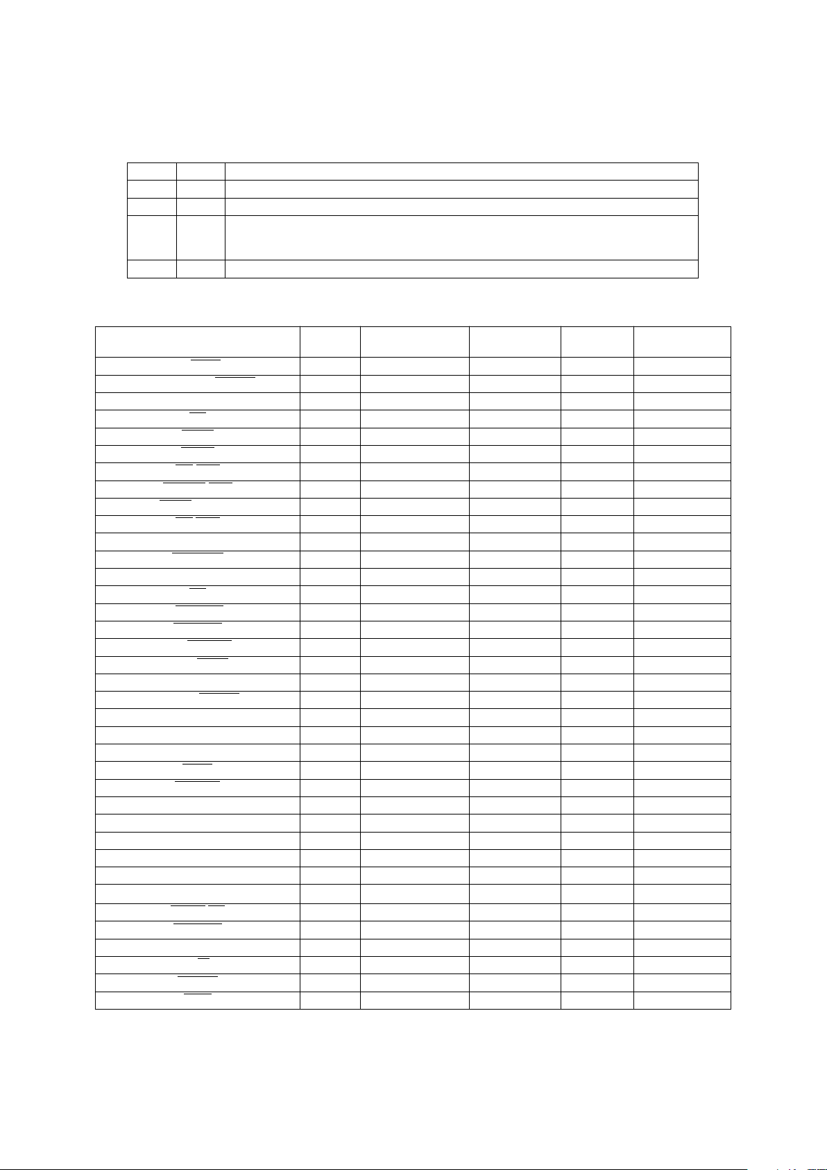
The following tables are a summary of the functional characteristics of MCU pins. Table 3-1 shows types of output drivers. Table 3-2 shows all inputs and outputs. Digital
inputs and outputs use CMOS logic levels. An entry in the Discrete I/O column indicates that a pin can also be used for general-purpose input, output, or both. The I/O
port designation is given when it applies. Table 3-3 shows characteristics of power
pins. Refer to Figure 3-1 for port organization.
331 144-PIN QFP
V
SS
NC
FC0/CS3
FC1/CS4
FC2/CS5
ADDR19/CS6
ADDR20/CS7
ADDR21/CS8
ADDR22/CS9
ADDR23/CS10
V
DD
PCLK
PWMB
PWMA
NC
NC
NC
NC
PAI
PGP6/OC4
V
DD
V
SS
NC
PGP5/OC3/OC1
PGP4/OC2/OC1
PGP3/OC1
MC68331
NC
PE4/AS
PE6/SIZ0
PE7/SIZ1
R/W
PF0/MODCLK
PF1/IRQ1
PF2/IRQ2
PF3/IRQ3
PF4/IRQ4
PF5/IRQ5
PF6/IRQ6
PF7/IRQ7
BERR
HALT
RESET
CLKOUT
NC
XFC
EXTAL
V
DD
XTAL
FREEZE/QUOT
TSC
BKPT/DSCLK
IFETCH/DSI
IPIPE/DSO
RXD
PQS7/TXD
V
SS
NC
PGP2/IC3
PGP1/IC2
PGP0/IC1
NC
NC
2
1
3
4
5
6
7
8
9
10
11
12
13
14
15
16
17
18
19
20
21
22
23
24
25
26
27
28
29
30
107
108
106
105
104
103
102
101
100
99
98
97
96
95
94
93
92
91
90
89
88
87
86
85
84
83
82
81
80
79
78
77
76
75
74
73
31
32
33
34
35
36
BGACK/CS2
BG/CS1
BR/CS0
CSBOOT
DATA0
DATA1
DATA2
DATA3
DATA4
DATA5
DATA6
DATA7NCDATA8NCDATA9
DATA10NCDATA11
VSSDATA12
DATA13
DATA14
DATA15
ADDR0
PE0/DSACK0
PE1/DSACK1
PE2/AVEC
PE3/RMC
PE5/DS
V
DD
NC
ADDR1
ADDR2
ADDR3
ADDR4
ADDR5
ADDR6
ADDR7
ADDR8
V
DD
V
SS
ADDR9
ADDR10
ADDR11
ADDR12
NC
NC
ADDR13
ADDR14
ADDR15NCADDR16
ADDR17
ADDR18
PQS0/MISO
PQS1/MOSI
PQS2/SCK
PQS3/PCS0/SS
PQS4/PCS1
PQS5/PCS2
PQS6/PCS3
143
144
142
141
140
139
138
137
136
135
134
133
132
131
130
129
128
127
126
125
124
123
122
121
120
119
118
117
116
115
114
113
112
111
110
109
37
65
68
383940414243444546474849505152535455565758596061626364666769707172
V
SS
V
DD
V
SS
V
DD
V
SS
V
DD
V
DD
V
SS
V
SS
V
DD
V
SS
VSSV
DD
V
DD
V
SS
V
DD
V
SS
V
SS
V
DD
P7/IC4/OC5/OC1
MOTOROLA OVERVIEW MC68331
3-6 USER’S MANUAL
3
Table 3-1 MCU Driver Types
Type I/O Description
A O Output-only signals that are always driven; no external pull-up required
Aw O Type A output with weak P-channel pull-up during reset
B O Three-state output that includes circuitry to pull up output before high impedance is
established, to ensure rapid rise time. An external holding resistor is required to maintain
logic level while the pin is in the high-impedance state.
Bo O Type B output that can be operated in an open-drain mode
Table 3-2 MCU Pin Characteristics
Pin
Mnemonic
Output
Driver
Input
Synchronized
Input
Hysteresis
Discrete
I/O
Port
Designation
ADDR23/CS10
/ECLK A Y N O —
ADDR[22:19]/CS[9:6]
A Y N O PC[6:3]
ADDR[18:0] A Y N — —
AS
B Y N I/O PE5
A
VEC B Y N I/O PE2
BERR
B Y N — —
BG
/CS1 B — — — —
BGA
CK/CS2 B Y N — —
BKPT
/DSCLK — Y Y — —
BR
/CS0 B Y N — —
CLKOUT A — — — —
CSBOO
T B — — — —
DATA[15:0]1 Aw Y N — —
DS
B Y N I/O PE4
DSA
CK1 B Y N I/O PE1
DSA
CK0 B Y N I/O PE0
DSI/IFETCH
A Y Y — —
DSO/IPIPE
A — — — —
EXTAL2 — — Special — —
FC[2:0]/CS[5:3]
A Y N O PC[2:0]
FREEZE/QUOT A — — — —
IC4/OC5 A Y Y I/O GP4
IC[3:1] A Y Y I/O GP[7:5]
HAL
T Bo Y N — —
IRQ[7:1]
B Y Y I/O PF[7:1]
MISO Bo Y Y I/O PQS0
MODCLK
1
B Y N I/O PF0
MOSI Bo Y Y I/O PQS1
OC[4:1] A Y Y I/O GP[3:0]
PAI
2
— Y Y I —
PCLK
2
— Y Y I —
PCSO
/SS Bo Y Y I/O PQS3
PCS[3:1]
Bo Y Y I/O PQS[6:4]
PWMA, PWMB A — — O —
R/W
A Y N — —
RESET
Bo Y Y — —
RMC
B Y N I/O PE3

MC68331 OVERVIEW MOTOROLA
USER’S MANUAL 3-7
3
3.4 Signal Descriptions
The following tables define MCU signals. Table 3-4 shows signal origin, type, and active state. Table 3-5 describes signal functions. Both tables are sorted alphabetically
by mnemonic. MCU pins often have multiple functions. More than one description can
apply to a pin.
1. DATA[15:0] are synchronized during reset only. MODCLK is synchronized only when used as an input port pin.
2. EXTAL, XFC, and XTAL are clock reference connections.
3. PAI and PCLK can be used for discrete input, but are not part of an I/O port.
RXD — N N — —
SCK Bo Y Y I/O PQS2
SIZ[1:0] B Y N I/O PE[7:6]
TSC — Y Y — —
TXD Bo Y Y I/O PQS7
XFC
3
— — — Special —
XTAL
3
— — — Special —
Table 3-3 MCU Power Connections
Pin Mnemonic Description
V
DDSYN
Clock Synthesizer Power
V
SSE/VDDE
External Periphery Power (Source and Drain)
V
SS
I/V
DDI
Internal Module Power (Source and Drain)
Table 3-4 Signal Characteristics
Signal
Name
MCU
Module
Signal
Type
Active
State
ADDR[23:0] SIM Bus —
AS
SIM Output 0
A
VEC SIM Input 0
BERR
SIM Input 0
BG
SIM Output 0
BGA
CK SIM Input 0
BKPT
CPU32 Input 0
BR
SIM Input 0
CLKOUT SIM Output —
CS[10:0]
SIM Output 0
CSBOO
T SIM Output 0
DATA[15:0] SIM Bus —
DS
SIM Output 0
DSA
CK[1:0] SIM Input 0
DSCLK CPU32 Input Serial Clock
DSI CPU32 Input (Serial Data)
DSO CPU32 Output (Serial Data)
EXTAL SIM Input —
Table 3-2 MCU Pin Characteristics (Continued)
Pin
Mnemonic
Output
Driver
Input
Synchronized
Input
Hysteresis
Discrete
I/O
Port
Designation

MOTOROLA OVERVIEW MC68331
3-8 USER’S MANUAL
3
FC[2:0] SIM Output —
FREEZE SIM Output 1
HAL
T SIM Input/Output 0
IC[4:1] GPT Input —
IFETCH
CPU32 Output —
IPIPE
CPU32 Output —
IRQ[7:1]
SIM Input 0
MISO QSM Input/Output —
MODCLK SIM Input —
MOSI QSM Input/Output —
OC[5:1] GPT Output —
PAI GPT Input —
PC[6:0] SIM Output (Port)
PCS[3:0] QSM Input/Output —
PE[7:0] SIM Input/Output (Port)
PF[7:0] SIM Input/Output (Port)
PGP[7:0] GPT Input/Output (Port)
PQS[7:0] QSM Input/Output (Port)
PCLK GPT Input —
PWMA, PWMB GPT Output —
QUOT SIM Output —
RESET
SIM Input/Output 0
RMC
SIM Output 0
R/W
SIM Output 1/0
RXD QSM Input —
SCK QSM Input/Output —
SIZ[1:0] SIM Output —
SS
QSM Input 0
TSC SIM Input —
TXD QSM Output —
XFC SIM Input —
XTAL SIM Output —
Table 3-5 Signal Function
Signal Name Mnemonic Function
Address Bus ADDR[23:0] 24-bit address bus
Address Strobe AS
Indicates that a valid address is on the address bus
Autovector A
VEC Requests an automatic vector during interrupt acknowledge
Bus Error BERR
Indicates that a bus error has occurred
Bus Grant BG
Indicates that the MCU has relinquished the bus
Bus Grant Acknowledge BGA
CK Indicates that an external device has assumed bus mastership
Breakpoint BKPT
Signals a hardware breakpoint to the CPU
Bus Request BR
Indicates that an external device requires bus mastership
System Clockout CLKOUT System clock output
Chip Selects CS[10:0]
Select external devices at programmed addresses
Boot Chip Select CSBOO
T Chip select for external boot start-up ROM
Data Bus DATA[15:0] 16-bit data bus
Table 3-4 Signal Characteristics (Continued)
Signal
Name
MCU
Module
Signal
Type
Active
State

MC68331 OVERVIEW MOTOROLA
USER’S MANUAL 3-9
3
Data Strobe DS During a read cycle, indicates when it is possible for an external
device to place data on the data bus. During a write cycle,
indicates that valid data is on the data bus.
Data and Size Acknowledge DSA
CK[1:0] Provide asynchronous data transfers and dynamic bus sizing
Development Serial In, Out, Clock DSI, DSO,
DSCLK
Serial I/O and clock for background debugging mode
Crystal Oscillator EXTAL, XTAL Connections for clock synthesizer circuit reference; a crystal or an
external oscillator can be used
Function Codes FC[2:0] Identify processor state and current address space
Freeze FREEZE Indicates that the CPU has entered background mode
Halt HAL
T Suspend external bus activity
Input Capture IC[3:1] When a specified transition is detected on an input capture pin, the
value in an internal GPT counter is latched
Input Capture 4/
Output Compare 5
IC4/OC5 Can be configured for either an input capture or output compare
Instruction Pipeline IPIPE
, IFETCH Indicate instruction pipeline activity
Interrupt Request Level IRQ[7:1]
Provides an interrupt priority level to the CPU
Master In Slave Out MISO Serial input to QSPI in master mode; serial output from QSPI in
slave mode
Clock Mode Select MODCLK Selects the source and type of system clock
Master Out Slave In MOSI Serial output from QSPI in master mode; serial input to QSPI in
slave mode
Output Compare OC[5:1] Change state when the value of an internal GPT counter matches
a value stored in a GPT control register
Pulse Accumulator Input PAI Signal input to the pulse accumulator
Port C PC[6:0] SIM digital output port signals
Auxiliary Timer Clock Input PCLK External clock dedicated to the GPT
Peripheral Chip Select PCS[3:0] QSPI peripheral chip selects
Port E PE[7:0] SIM digital I/O port signals
Port F PF[7:0] SIM digital I/O port signals
Port GP PGP[7:0] GPT digital I/O port signals
Port QS PQS[7:0] QSM digital I/O port signals
Pulse-Width Modulation PWMA, PWMB Output for PWM
Quotient Out QUOT Provides the quotient bit of the polynomial divider
Reset RESET
System reset
Read-Modify-Write Cycle RMC
Indicates an indivisible read-modify-write instruction
Read/Write R/W
Indicates the direction of data transfer on the bus
SCI Receive Data RXD Serial input to the SCI
QSPI Serial Clock SCK Clock output from QSPI in master mode; clock input to QSPI in
slave mode
Size SIZ[1:0] Indicates the number of bytes to be transferred during a bus cycle
Slave Select SS
Causes serial transmission when QSPI is in slave mode; causes
mode fault in master mode
Three-State Control TSC Places all output drivers in a high-impedance state
SCI Transmit Data TXD Serial output from the SCI
External Filter Capacitor XFC Connection for external phase-locked loop filter capacitor
Table 3-5 Signal Function (Continued)
Signal Name Mnemonic Function

MOTOROLA OVERVIEW MC68331
3-10 USER’S MANUAL
3
3.5 Intermodule Bus
The intermodule bus (IMB) is a standardized bus developed to facilitate both design
and operation of modular microcontrollers. It contains circuitry to support exception
processing, address space partitioning, multiple interrupt levels, and vectored interrupts. The standardized modules in the MCU communicate with one another and with
external components through the IMB. The IMB in the MCU uses 24 address and 16
data lines.
3.6 System Memory Map
Figure 3-4, Figure 3-5, Figure 3-6, Figure 3-7, and Figure 3-8 are MCU memory
maps. Figure 3-4 shows IMB addresses of internal registers. Figure 3-5 through Figure 3-8 show system memory maps that use different external decoding schemes.
3.6.1 Internal Register Map
In Figure 3-4, IMB ADDR[23:20] are represented by the letter Y. The value represent-
ed by Y determines the base address of MCU module control registers. In M68300 microcontrollers, Y is equal to M111, where M is the logic state of the module mapping
(MM) bit in the system integration module configuration register (SIMCR).
3.6.2 Address Space Maps
Figure 3-5 shows a single memory space. Function codes FC[2:0] are not decoded
externally so that separate user/supervisor or program/data spaces are not provided.
In Figure 3-6, FC2 is decoded, resulting in separate supervisor and user spaces.
FC[1:0] are not decoded, so that separate program and data spaces are not provided.
In Figure 3-7 and Figure 3-8, FC[2:0] are decoded, resulting in four separate memory
spaces: supervisor/program, supervisor/data, user/program and user/data.
All exception vectors are located in supervisor data space, except the reset vector,
which is located in supervisor program space. Only the initial reset vector is fixed in
the processor's memory map. Once initialization is complete, there are no fixed assignments. Since the vector base register (VBR) provides the base address of the vector table, the vector table can be located anywhere in memory. Refer to SECTION 5
CENTRAL PROCESSING UNIT for more information concerning memory management, extended addressing, and exception processing. Refer to SECTION 4 SYSTEM
INTEGRATION MODULE for more information concerning function codes and address space types.

MC68331 OVERVIEW MOTOROLA
USER’S MANUAL 3-11
3
Figure 3-4 Internal Register Memory Map
331 ADDRESS MAP
SIM
RESERVED
QSM
$YFFA00
$YFF000
$YFF93F
$YFF900
$YFFFFF
$YFFC00
$YFFDFF
$YFFAFF
$YFFA80
$YFFA7F
GPT
Y = M111, where M is the state of the module mapping (MM) bit in the SIM configuration register.

MOTOROLA OVERVIEW MC68331
3-12 USER’S MANUAL
3
Figure 3-5 Overall Memory Map
331 S/U COMB MAP
INTERNAL REGISTERS (MM = 1)
$000000
$FFFFFF
$FF0000
COMBINED
SUPERVISOR
AND USER
SPACE
$7FF000
INTERNAL REGISTERS (MM = 0)
NOTES:
1. Location of the exception vector table is determined by the vector base register. The vector address is the sum of the vector
base register and the vector offset.
2. Location of the module control registers is determined by the state of the module mapping (MM) bit in the SIM configuration register.
Y = M111, where M is the state of the MM bit.
3. Unused addresses within the internal register block are mapped externally. "RESERVED" blocks are not mapped externally.
$XX03FC
$XX0000RESET — INITIAL STACK POINTER
RESET — INITIAL PC
BUS ERROR
ADDRESS ERROR
ILLEGAL INSTRUCTION
ZERO DIVISION
CHK, CHK2 INSTRUCTIONS
TRAPcc, TRAPV INSTRUCTIONS
PRIVILEGE VIOLATION
TRACE
LINE 1010 EMULATOR
LINE 1111 EMULATOR
HARDWARE BREAKPOINT
(RESERVED COPROCESSOR PROTOCOL VIOLATION)
FORMAT ERROR AND UNINITIALIZED INTERRUPT
FORMAT ERROR AND UNINITIALIZED INTERRUPT
(UNASSIGNED, RESERVED)
SPURIOUS INTERRUPT
LEVEL 1 INTERRUPT AUTOVECTOR
LEVEL 2 INTERRUPT AUTOVECTOR
LEVEL 3 INTERRUPT AUTOVECTOR
LEVEL 4 INTERRUPT AUTOVECTOR
LEVEL 5 INTERRUPT AUTOVECTOR
LEVEL 6 INTERRUPT AUTOVECTOR
LEVEL 7 INTERRUPT AUTOVECTOR
TAP INSTRUCTION VECTORS (0–15)
(RESERVED, COPROCESSOR)
(UNASSIGNED, RESERVED)
USER-DEFINED VECTORS
0000
0004
0008
000C
0010
0014
0018
001C
0020
0024
0028
002C
0030
0034
0038
003C
0040–005C
006C
0064
0068
006C
0070
0074
0078
007C
0080–00BC
00C0–00EB
00EC–00FC
0100–03FC
VECTOR
OFFSET
0
1
2
3
4
5
6
7
8
9
10
11
12
13
14
15
16–23
24
25
26
27
28
29
30
31
32–47
48–58
59–63
64–255
VECTOR
NUMBER
TYPE OF
EXCEPTION
$YFF000
$YFF93F
GPT
$YFFA00
RESERVED
$YFFAFF
$YFFA7F
SIM
$YFFA80
RESERVED
$YFFC00
$YFFFFF
QSM
$YFF900
$YFFDFF

MC68331 OVERVIEW MOTOROLA
USER’S MANUAL 3-13
3
Figure 3-6 Separate Supervisor and User Space Map
331 S/U SEP MAP
INTERNAL REGISTERS
$000000
$FFFFFF
$FF0000
SUPERVISOR
SPACE
$7FF000
INTERNAL REGISTERS
NOTES:
1. Location of the exception vector table is determined by the vector base register. The vector address is the sum of the vector
base register and the vector offset.
2. Location of the module control registers is determined by the state of the module mapping (MM) bit in the SIM configuration register.
Y = M111, where M is the state of the MM bit.
3. Unused addresses within the internal register block are mapped externally. "RESERVED" blocks are not mapped externally.
$XX03FC
$XX0000RESET — INITIAL STACK POINTER
RESET — INITIAL PC
BUS ERROR
ADDRESS ERROR
ILLEGAL INSTRUCTION
ZERO DIVISION
CHK, CHK2 INSTRUCTIONS
TRAPcc, TRAPV INSTRUCTIONS
PRIVILEGE VIOLATION
TRACE
LINE 1010 EMULATOR
LINE 1111 EMULATOR
HARDWARE BREAKPOINT
(RESERVED COPROCESSOR PROTOCOL VIOLATION)
FORMAT ERROR AND UNINITIALIZED INTERRUPT
FORMAT ERROR AND UNINITIALIZED INTERRUPT
(UNASSIGNED, RESERVED)
SPURIOUS INTERRUPT
LEVEL 1 INTERRUPT AUTOVECTOR
LEVEL 2 INTERRUPT AUTOVECTOR
LEVEL 3 INTERRUPT AUTOVECTOR
LEVEL 4 INTERRUPT AUTOVECTOR
LEVEL 5 INTERRUPT AUTOVECTOR
LEVEL 6 INTERRUPT AUTOVECTOR
LEVEL 7 INTERRUPT AUTOVECTOR
TAP INSTRUCTION VECTORS (0–15)
(RESERVED, COPROCESSOR)
(UNASSIGNED, RESERVED)
USER-DEFINED VECTORS
0000
0004
0008
000C
0010
0014
0018
001C
0020
0024
0028
002C
0030
0034
0038
003C
0040–005C
006C
0064
0068
006C
0070
0074
0078
007C
0080–00BC
00C0–00EB
00EC–00FC
0100–03FC
VECTOR
OFFSET
0
1
2
3
4
5
6
7
8
9
10
11
12
13
14
15
16–23
24
25
26
27
28
29
30
31
32–47
48–58
59–63
64–255
VECTOR
NUMBER
TYPE OF
EXCEPTION
INTERNAL REGISTERS
INTERNAL REGISTERS
USER
SPACE
$000000
$7FF000
4
$FF0000
4
$FFFFFF
4. Some internal registers are not available in user space.
$YFF000
$YFF93F
GPT
$YFFA00
RESERVED
$YFFAFF
$YFFA7F
SIM
$YFFA80
RESERVED
$YFFC00
$YFFFFF
QSM
$YFF900
$YFFDFF

MOTOROLA OVERVIEW MC68331
3-14 USER’S MANUAL
3
Figure 3-7 Supervisor Space (Separate Program/Data Space) Map
331 SUPER P/D MAP
INTERNAL REGISTERS
$000000
$FFFFFF
$FF0000
$7FF000
INTERNAL REGISTERS
NOTES:
1. Location of the exception vector table is determined by the vector base register. The vector address is the sum of the vector
base register and the vector offset.
2. Location of the module control registers is determined by the state of the module mapping (MM) bit in the SIM configuration register.
Y = M111, where M is the state of the MM bit.
3. Unused addresses within the internal register block are mapped externally. "RESERVED" blocks are not mapped externally.
$XX03FC
$XX0000RESET — INITIAL STACK POINTER
RESET — INITIAL PC
BUS ERROR
ADDRESS ERROR
ILLEGAL INSTRUCTION
ZERO DIVISION
CHK, CHK2 INSTRUCTIONS
TRAPcc, TRAPV INSTRUCTIONS
PRIVILEGE VIOLATION
TRACE
LINE 1010 EMULATOR
LINE 1111 EMULATOR
HARDWARE BREAKPOINT
(RESERVED COPROCESSOR PROTOCOL VIOLATION)
FORMAT ERROR AND UNINITIALIZED INTERRUPT
FORMAT ERROR AND UNINITIALIZED INTERRUPT
(UNASSIGNED, RESERVED)
SPURIOUS INTERRUPT
LEVEL 1 INTERRUPT AUTOVECTOR
LEVEL 2 INTERRUPT AUTOVECTOR
LEVEL 3 INTERRUPT AUTOVECTOR
LEVEL 4 INTERRUPT AUTOVECTOR
LEVEL 5 INTERRUPT AUTOVECTOR
LEVEL 6 INTERRUPT AUTOVECTOR
LEVEL 7 INTERRUPT AUTOVECTOR
TAP INSTRUCTION VECTORS (0–15)
(RESERVED, COPROCESSOR)
(UNASSIGNED, RESERVED)
USER-DEFINED VECTORS
0000
0004
0008
000C
0010
0014
0018
001C
0020
0024
0028
002C
0030
0034
0038
003C
0040–005C
006C
0064
0068
006C
0070
0074
0078
007C
0080–00BC
00C0–00EB
00EC–00FC
0100–03FC
VECTOR
OFFSET
0
1
2
3
4
5
6
7
8
9
10
11
12
13
14
15
16–23
24
25
26
27
28
29
30
31
32–47
48–58
59–63
64–255
VECTOR
NUMBER
$000000
$FFFFFF
4. Some internal registers are not available in user space.
$XX0004
$XX0000
RESET — INITIAL STACK POINTER
RESET — INITIAL PC
0000
0004
VECTOR
OFFSET
0
1
VECTOR
NUMBER
EXCEPTION VECTORS LOCATED
IN SUPERVISOR PROGRAM SPACE
EXCEPTION VECTORS LOCATED
IN SUPERVISOR DATA SPACE
SUPERVISOR
DATA
SPACE
SUPERVISOR
PROGRAM
SPACE
$YFF000
$YFF93F
GPT
$YFFA00
RESERVED
$YFFAFF
$YFFA7F
SIM
$YFFA80
RESERVED
$YFFC00
$YFFFFF
QSM
$YFF900
$YFFDFF

MC68331 OVERVIEW MOTOROLA
USER’S MANUAL 3-15
3
Figure 3-8 User Space (Separate Program/Data Space) Map
331 USER P/D MAP
INTERNAL REGISTERS
$000000
$FFFFFF
$FF0000
$7FF000
INTERNAL REGISTERS
NOTES:
1. Location of the module control registers is determined by the state of the module mapping (MM) bit in the SIM configuration
register. Y = M111, where M is the state of the MM bit.
2. Unused addresses within the internal register block are mapped externally. "RESERVED" blocks are not mapped externally.
3. Some internal registers are not available in user space.
$000000
$FFFFFF
USER
DATA
SPACE
USER
PROGRAM
SPACE
$YFF000
$YFF93F
GPT
$YFFA00
RESERVED
$YFFAFF
$YFFA7F
SIM
$YFFA80
RESERVED
$YFFC00
$YFFFFF
QSM
$YFF900
$YFFDFF

MOTOROLA OVERVIEW MC68331
3-16 USER’S MANUAL
3
3.7 System Reset
The following information is a concise reference only. System reset is a complex operation. To understand operation during and after reset, refer to SECTION 4 SYSTEM
INTEGRATION MODULE, paragraph 4.6 Reset for a more complete discussion of the
reset function.
3.7.1 SIM Reset Mode Selection
The logic states of certain data bus pins during reset determine SIM operating configuration. In addition, the state of the MODCLK pin determines system clock source and
the state of the BKPT
pin determines what happens during subsequent breakpoint as-
sertions. Table 3-6 is a summary of reset mode selection options.
Table 3-6 SIM Reset Mode Selection
Mode Select Pin Default Function
(Pin Left High)
Alternate Function
(Pin Pulled Low)
DATA0 CSBOO
T 16-Bit CSBOOT 8-Bit
DATA1 CS0
CS1
CS2
BRBG
BGACK
DATA2 CS3
CS4
CS5
FC0FC1FC2
DATA3
DATA4
DATA5
DATA6
DATA7
CS6
CS[7:6]
CS[8:6]
CS[9:6]
CS[10:6]
ADDR19
ADDR[20:19]
ADDR[21:19]
ADDR[22:19]
ADDR[23:19]
DATA8 DSA
CK0, DSACK1,
A
VEC, DS, AS,
SIZ[1:0]
PORTE
DATA9 IRQ[7:1]
, MODCLK PORTF
DATA11 Test Mode Disabled Test Mode Enabled
MODCLK VCO = System Clock EXTAL = System Clock
BKPT
Background Mode Disabled Background Mode Enabled

MC68331 OVERVIEW MOTOROLA
USER’S MANUAL 3-17
3
3.7.2 MCU Module Pin Function During Reset
Generally, pins associated with modules other than the SIM default to port functions,
and input/output ports are set to input state. This is accomplished by disabling pin
functions in the appropriate control registers, and by clearing the appropriate port data
direction registers. Refer to individual module sections in this manual for more information. Table 3-7 is a summary of module pin function out of reset.
Table 3-7 Module Pin Functions
Module Pin Mnemonic Function
CPU32 DSI/IFETCH
DSI/IFETCH
DSO/IPIPE DSO/IPIPE
BKPT/DSCLK BKPT/DSCLK
GPT PGP7/IC4/OC5 Discrete Input
PGP[6:3]/OC[4:1] Discrete Input
PGP[2:0]/IC[3:1] Discrete Input
PAI Discrete Input
PCLK Discrete Input
PWMA, PWMB Discrete Output
QSM PQS7/TXD Discrete Input
PQS[6:4]/PCS[3:1] Discrete Input
PQS3/PCS0/SS
Discrete Input
PQS2/SCK Discrete Input
PQS1/MOSI Discrete Input
PQS0/MISO Discrete Input
RXD RXD

MOTOROLA OVERVIEW MC68331
3-18 USER’S MANUAL
3

MC68331 SYSTEM INTEGRATION MODULE MOTOROLA
USER’S MANUAL 4-1
4
SECTION 4 SYSTEM INTEGRATION MODULE
This section is an overview of SIM function. Refer to the
SIM Reference Manual
(SIMRM/AD) for a comprehensive discussion of SIM capabilities. Refer to APPENDIX D
REGISTER SUMMARY for information concerning the SIM address map and register
structure.
4.1 General
The system integration module (SIM) consists of five functional blocks. Figure 4-1 is
a block diagram of the SIM.
The system configuration and protection block controls configuration parameters and
provides bus and software watchdog monitors. In addition, it provides a periodic interrupt generator to support execution of time-critical control routines.
The system clock generates clock signals used by the SIM, other IMB modules, and
external devices.
The external bus interface handles the transfer of information between IMB modules
and external address space. EBI pins can also be configured for use as general-purpose I/O ports E and F.
The chip-select block provides 12 chip-select signals. Each chip-select signal has an
associated base register and option register that contain the programmable characteristics of that chip select. Chip-select pins can also be configured for use as generalpurpose output port C.
The system test block incorporates hardware necessary for testing the MCU. It is used
to perform factory tests, and its use in normal applications is not supported.

MOTOROLA SYSTEM INTEGRATION MODULE MC68331
4-2 USER’S MANUAL
4
Figure 4-1 System Integration Module Block Diagram
4.2 System Configuration and Protection
The system configuration and protection functional block controls module configuration, preserves reset status, monitors internal activity, and provides periodic interrupt
generation. Figure 4-2 is a block diagram of the submodule.
S(C)IM BLOCK
SYSTEM CONFIGURATION
AND PROTECTION
CLOCK SYNTHESIZER
CHIP SELECTS
EXTERNAL BUS INTERFACE
FACTORY TEST
CLKOUT
EXTAL
MODCLK
CHIP SELECTS
EXTERNAL BUS
RESET
TSC
FREEZE/QUOT

MC68331 SYSTEM INTEGRATION MODULE MOTOROLA
USER’S MANUAL 4-3
4
Figure 4-2 System Configuration and Protection
4.2.1 Module Mapping
Control registers for all the modules in the microcontroller are mapped into a 4-Kbyte
block. The state of the module mapping bit (MM) in the SIM module configuration register (SIMCR) determines where the control register block is located in the system
memory map. When MM = 0, register addresses range from $7FF000 to $7FFFFF;
when MM = 1, register addresses range from $FFF000 to $FFFFFF.
4.2.2 Interrupt Arbitration
Each module that can generate interrupt requests has an interrupt arbitration (IARB)
field. Arbitration between interrupt requests of the same priority is performed by serial
contention between IARB field bit values. Contention must take place whenever an interrupt request is acknowledged, even when there is only a single request pending.
For an interrupt to be serviced, the appropriate IARB field must have a non-zero value.
If an interrupt request from a module with an IARB field value of %0000 is recognized,
the CPU32 processes a spurious interrupt exception.
SYS PROTECT BLOCK
MODULE CONFIGURATION
AND TEST
RESET STATUS
HALT MONITOR
BUS MONITOR
SPURIOUS INTERRUPT MONITOR
SOFTWARE WATCHDOG TIMER
PERIODIC INTERRUPT TIMER
PRESCALER
CLOCK
BERR
RESET REQUEST
RESET
REQUEST
2
9
IRQ [7:1]

MOTOROLA SYSTEM INTEGRATION MODULE MC68331
4-4 USER’S MANUAL
4
Because the SIM routes external interrupt requests to the CPU32, the SIM IARB field
value is used for arbitration between internal and external interrupts of the same priority. The reset value of IARB for the SIM is %1111, and the reset IARB value for all
other modules is %0000, which prevents SIM interrupts from being discarded during
initialization. Refer to 4.7 Interrupts for a discussion of interrupt arbitration.
4.2.3 Show Internal Cycles
A show cycle allows internal bus transfers to be monitored externally. The SHEN field
in the SIMCR determines what the external bus interface does during internal transfer
operations. Table 4-1 shows whether data is driven externally, and whether external
bus arbitration can occur. Refer to 4.5.6.2 Show Cycles for more information.
4.2.4 Factory Test Mode
The internal IMB can serve as slave to an external master for direct module testing.
This test mode is reserved for factory test. Slave mode is enabled by holding DATA11
low during reset. The slave enabled (SLVEN) bit is a read-only bit that shows the reset
state of DATA11.
4.2.5 Register Access
The CPU32 can operate at either of two privilege levels. Supervisor level is more privileged than user level — all instructions and system resources are available at supervisor level, but access is restricted at user level. Effective use of privilege level can
protect system resources from uncontrolled access. The state of the S bit in the CPU
status register determines access level, and whether the user or supervisor stack
pointer is used for stacking operations. The SUPV bit places SIM global registers in
either supervisor or user data space. When SUPV = 0, registers with controlled access
are accessible from either the user or supervisor privilege level; when SUPV = 1, registers with controlled access are restricted to supervisor access only.
4.2.6 Reset Status
The reset status register (RSR) latches internal MCU status during reset. Refer to
4.6.9 Reset Status Register for more information.
4.2.7 Bus Monitor
The internal bus monitor checks data and size acknowledge (DSACK
) or autovector
(AVEC
) signal response times during normal bus cycles. The monitor asserts the in-
ternal bus error (BERR
) signal when the response time is excessively long.
Table 4-1 Show Cycle Enable Bits
SHEN Action
00 Show cycles disabled, external arbitration enabled
01 Show cycles enabled, external arbitration disabled
10 Show cycles enabled, external arbitration enabled
11 Show cycles enabled, external arbitration enabled;
internal activity is halted by a bus grant

MC68331 SYSTEM INTEGRATION MODULE MOTOROLA
USER’S MANUAL 4-5
4
DSACK and AVEC response times are measured in clock cycles. Maximum allowable
response time can be selected by setting the bus monitor timing (BMT) field in the system protection control register (SYPCR). Table 4-2 shows the periods allowed.
The monitor does not check DSACK
response on the external bus unless the CPU32
initiates a bus cycle. The BME bit in SYPCR enables the internal bus monitor for internal to external bus cycles. If a system contains external bus masters, an external bus
monitor must be implemented and the internal-to-external bus monitor option must be
disabled.
When monitoring transfers to an 8-bit port, the bus monitor does not reset until both
byte accesses of a word transfer are completed. Monitor time-out period must be at
least twice the number of clocks that a single byte access requires.
4.2.8 Halt Monitor
The halt monitor responds to an assertion of the HALT
signal on the internal bus. Refer
to 4.5.5.2 Double Bus Faults for more information. Halt monitor reset can be inhibited
by the halt monitor (HME) bit in SYPCR.
4.2.9 Spurious Interrupt Monitor
During interrupt exception processing, the CPU32 normally acknowledges an interrupt
request, recognizes the highest priority source, and then acquires a vector or responds to a request for autovectoring. The spurious interrupt monitor asserts the internal bus error signal (BERR
) if no interrupt arbitration occurs during interrupt
exception processing. The assertion of BERR
causes the CPU32 to load the spurious
interrupt exception vector into the program counter. The spurious interrupt monitor
cannot be disabled. Refer to 4.7 Interrupts for further information. For detailed information about interrupt exception processing, refer to SECTION 5 CENTRAL PRO-
CESSING UNIT.
4.2.10 Software Watchdog
The software watchdog is controlled by the software watchdog enable (SWE) bit in
SYPCR. When enabled, the watchdog requires that a service sequence be written to
software service register SWSR on a periodic basis. If servicing does not take place,
the watchdog times out and asserts the reset signal.
Perform a software watchdog service sequence as follows:
1. Write $55 to SWSR.
2. Write $AA to SWSR.
Table 4-2 Bus Monitor Period
BMT Bus Monitor Time-Out Period
00 64 System Clocks
01 32 System Clocks
10 16 System Clocks
11 8 System Clocks

MOTOROLA SYSTEM INTEGRATION MODULE MC68331
4-6 USER’S MANUAL
4
Both writes must occur before time-out in the order listed, but any number of instructions can be executed between the two writes.
Watchdog clock rate is affected by the software watchdog prescale (SWP) and software watchdog timing (SWT) fields in SYPCR.
SWP determines system clock prescaling for the watchdog timer and determines that
one of two options, either no prescaling or prescaling by a factor of 512, can be selected. The value of SWP is affected by the state of the MODCLK pin during reset, as
shown in Table 4-3. System software can change SWP value.
The SWT field selects the divide ratio used to establish software watchdog time-out
period. Time-out period is given by the following equations.
or
Table 4-4 shows the ratio for each combination of SWP and SWT bits. When SWT[1:0]
are modified, a watchdog service sequence must be performed before the new timeout period can take effect.
Figure 4-3 is a block diagram of the watchdog timer and the clock control for the periodic interrupt timer.
Table 4-3 MODCLK Pin and SWP Bit During Reset
MODCLK SWP
0 (External Clock) 1 (÷ 512)
1 (Internal Clock) 0 (÷ 1)
Table 4-4 Software Watchdog Ratio
SWP SWT Ratio
000
2
9
001
2
11
010
2
13
011
2
15
100
2
18
101
2
20
110
2
22
111
2
24
Time-out Period
1
EXTAL Frequency Divide Ratio⁄
------------------------------------------------------------------------------------ -=
Time-out Period
Divide Ratio
EXTAL Frequency
------------------------------------------------ -=

MC68331 SYSTEM INTEGRATION MODULE MOTOROLA
USER’S MANUAL 4-7
4
Figure 4-3 Periodic Interrupt Timer and Software Watchdog Timer
4.2.11 Periodic Interrupt Timer
The periodic interrupt timer allows the generation of interrupts of specific priority at predetermined intervals. This capability is often used to schedule control system tasks
that must be performed within time constraints. The timer consists of a prescaler, a
modulus counter, and registers that determine interrupt timing, priority and vector assignment. Refer to SECTION 5 CENTRAL PROCESSING UNIT for further information
about interrupt exception processing.
The periodic interrupt modulus counter is clocked by a signal derived from the buffered
crystal oscillator (EXTAL) input pin unless an external frequency source is used. The
value of the periodic timer prescaler (PTP) bit in the periodic interrupt timer register
(PITR) determines system clock prescaling for the watchdog timer. One of two options, either no prescaling, or prescaling by a factor of 512, can be selected. The value
of PTP is affected by the state of the MODCLK pin during reset, as shown in Table 4-
5. System software can change PTP value.
Either clock signal (EXTAL or EXTAL ÷ 512) is divided by four before driving the modulus counter (PITCLK). The modulus counter is initialized by writing a value to the periodic timer modulus timer modulus (PITM) field in the PITR. A zero value turns off the
periodic timer. When the modulus counter value reaches zero, an interrupt is generated. The modulus counter is then reloaded with the value in PITM and counting repeats.
If a new value is written to PITR, it is loaded into the modulus counter when the current
count is completed.
Table 4-5 MODCLK Pin and PTP Bit at Reset
MODCLK PTP
0 (External Clock) 1 (÷ 512)
1 (Internal Clock) 0 (÷ 1)
CLOCK
DISABLE
PRESCALER (29)
CLOCK
MUX
EXTAL
LPSTOP
SWP
PTP
FREEZE
SWCLK
PITCLK
PRECLK
2
9
÷ 4
RESET
PIT
INTERRUPT
PITR
SWT1
SWT0
SWE
15 STAGE
DIVIDER CHAIN (2
15
)
2
11213215
8-BIT MODULUS
PIT BLOCK
COUNTER

MOTOROLA SYSTEM INTEGRATION MODULE MC68331
4-8 USER’S MANUAL
4
Use the following expression to calculate timer period.
Interrupt priority and vectoring are determined by the values of the periodic interrupt
request level (PIRQL) and periodic interrupt vector (PIV) fields in the periodic interrupt
control register (PICR).
Content of PIRQL is compared to the CPU32 interrupt priority mask to determine
whether the interrupt is recognized. Table 4-6 shows priority of PIRQL values. Because of SIM hardware prioritization, a PIT interrupt is serviced before an external interrupt request of the same priority. The periodic timer continues to run when the
interrupt is disabled.
The PIV field contains the periodic interrupt vector. The vector is placed on the IMB
when an interrupt request is made. The vector number used to calculate the address
of the appropriate exception vector in the exception vector table. Reset value of the
PIV field is $0F, which corresponds to the uninitialized interrupt exception vector.
4.2.12 Low-Power STOP Operation
When the CPU32 executes the LPSTOP instruction, the current interrupt priority mask
is stored in the clock control logic, internal clocks are disabled according to the state
of the STSIM bit in the SIMCR, and the MCU enters low-power stop mode. The bus
monitor, halt monitor, and spurious interrupt monitor are all inactive during low-power
stop.
During low-power stop, the clock input to the software watchdog timer is disabled and
the timer stops. The software watchdog begins to run again on the first rising clock
edge after low-power stop ends. The watchdog is not reset by low-power stop. A service sequence must be performed to reset the timer.
The periodic interrupt timer does not respond to the LPSTOP instruction, but continues
to run during LPSTOP. To stop the periodic interrupt timer, PITR must be loaded with
a zero value before the LPSTOP instruction is executed. A PIT interrupt, or an external
interrupt request, can bring the MCU out of the low-power stop condition if it has a
higher priority than the interrupt mask value stored in the clock control logic when lowpower stop is initiated. LPSTOP can be terminated by a reset.
Table 4-6 Periodic Interrupt Priority
PIRQL Priority Level
000 Periodic Interrupt Disabled
001 Interrupt Priority Level 1
010 Interrupt Priority Level 2
011 Interrupt Priority Level 3
100 Interrupt Priority Level 4
101 Interrupt Priority Level 5
110 Interrupt Priority Level 6
111 Interrupt Priority Level 7
PIT Period
PIT Modulus()Prescaler Value()4()
EXTAL Frequency
----------------------------------------------------------------------------------------------=

MC68331 SYSTEM INTEGRATION MODULE MOTOROLA
USER’S MANUAL 4-9
4
4.2.13 Freeze Operation
The FREEZE signal halts MCU operations during debugging. FREEZE is asserted internally by the CPU32 if a breakpoint occurs while background mode is enabled. When
FREEZE is asserted, only the bus monitor, software watchdog, and periodic interrupt
timer are affected. The halt monitor and spurious interrupt monitor continue to operate
normally. Setting the freeze bus monitor (FRZBM) bit in the SIMCR disables the bus
monitor when FREEZE is asserted, and setting the freeze software watchdog
(FRZSW) bit disables the software watchdog and the periodic interrupt timer when
FREEZE is asserted. When FRZSW is set, FREEZE assertion must be at least two
times the PIT clock source period to ensure an accurate number of PIT counts.
4.3 System Clock
The system clock in the SIM provides timing signals for the IMB modules and for an
external peripheral bus. Because the MCU is a fully static design, register and memory
contents are not affected when the clock rate changes. System hardware and software
support changes in clock rate during operation.
The system clock signal can be generated in one of three ways. An internal phaselocked loop can synthesize the clock from either an internal reference or an external
reference, or the clock signal can be input from an external frequency source. Keep
these clock sources in mind while reading the rest of this section. Figure 4-4 is a block
diagram of the system clock. Refer to APPENDIX A ELECTRICAL CHARACTERIS-
TICS for clock specifications.
Figure 4-4 System Clock Block Diagram
32 PLL BLOCK
CLKOUT
PHASE
COMPARATOR
LOW-PASS
FILTER
VCO
CRYSTAL
OSCILLATOR
SYSTEM
CLOCK
SYSTEM CLOCK CONTROL
FEEDBACK DIVIDER
W
X
Y
EXTAL XTAL XFC
V
DDSYN

MOTOROLA SYSTEM INTEGRATION MODULE MC68331
4-10 USER’S MANUAL
4
4.3.1 Clock Sources
The state of the clock mode (MODCLK) pin during reset determines clock source.
When MODCLK is held high during reset, the clock synthesizer generates a clock signal from either an internal or an external reference frequency — the clock synthesizer
control register (SYNCR) determines operating frequency and mode of operation.
When MODCLK is held low during reset, the clock synthesizer is disabled and an external system clock signal must be applied — SYNCR control bits have no effect.
To generate a reference frequency using the internal oscillator a reference crystal
must be connected between the EXTAL and XTAL pins. Figure 4-5 shows a recommended circuit.
Figure 4-5 System Clock Oscillator Circuit
If an external reference signal or an external system clock signal is applied via the EXTAL pin, the XTAL pin must be left floating. External reference signal frequency must
be less than or equal to maximum specified reference frequency. External system
clock signal frequency must be less than or equal to maximum specified system clock
frequency.
When an external system clock signal is applied (PLL disabled, MODCLK = 0 during
reset), the duty cycle of the input is critical, especially at operating frequencies close
to maximum. The relationship between clock signal duty cycle and clock signal period
is expressed:
4.3.2 Clock Synthesizer Operation
V
DDSYN
is used to power the clock circuits when either an internal or an external reference frequency is applied. A separate power source increases MCU noise immunity
and can be used to run the clock when the MCU is powered down. A quiet power supply must be used as the V
DDSYN
source. Adequate external bypass capacitors should
be placed as close as possible to the V
DDSYN
pin to assure stable operating frequen-
V
SSI
EXTAL
XTAL
22 pF*
C1
330k
R1
32 OSCILLATOR
Resistance and capacitance based on a test circuit constructed with a DAISHINKU DMX-38 32.768-kHz crystal.
Specific components must be based on crystal type. Contact crystal vendor for exact circuit.
*
22 pF*
C2
10M
R2
Minumum External Clock Period
Minimum External Clock High Low Time⁄
50% Percentage Variation of External Clock Input Duty Cycle–
----------------------------------------------------------------------------------------------------------------------------------------------------------------------=

MC68331 SYSTEM INTEGRATION MODULE MOTOROLA
USER’S MANUAL 4-11
4
cy. When an external system clock signal is applied and the PLL is disabled, V
DDSYN
should be connected to the VDD supply. Refer to the
SIM Reference Manual
(SIMRM/
AD) for more information regarding system clock power supply conditioning.
A voltage controlled oscillator (VCO) generates the system clock signal. To maintain
a 50% clock duty cycle, VCO frequency is either two or four times system clock frequency, depending on the state of the X bit in SYNCR. A portion of the clock signal is
fed back to a divider/counter. The divider controls the frequency of one input to a
phase comparator. The other phase comparator input is a reference signal, either from
the crystal oscillator or from an external source. The comparator generates a control
signal proportional to the difference in phase between the two inputs. The signal is lowpass filtered and used to correct VCO output frequency.
Filter geometry can vary, depending upon the external environment and required clock
stability. Figure 4-6 shows two recommended filters. XFC pin leakage must be as
specified in APPENDIX A ELECTRICAL CHARACTERISTICS to maintain optimum
stability and PLL performance.
An external filter network connected to the XFC pin is not required when an external
system clock signal is applied and the PLL is disabled. The XFC pin must be left floating in this case.
Figure 4-6 System Clock Filter Networks
The synthesizer locks when VCO frequency is equal to EXTAL frequency. Lock time
is affected by the filter time constant and by the amount of difference between the two
comparator inputs. Whenever comparator input changes, the synthesizer must relock.
Lock status is shown by the SLOCK bit in SYNCR. During power-up, the MCU does
not come out of reset state until the synthesizer locks. Crystal type, characteristic frequency, and layout of external oscillator circuitry affect lock time.
When the clock synthesizer is used, control register SYNCR determines operating frequency and various modes of operation. The SYNCR W bit controls a three-bit prescaler in the feedback divider. Setting W increases VCO speed by a factor of four. The
16/32 XFC CONN
1. Maintain low-leakage on the XFC node. See Appendix A electrical characteristics for more information.
2. Recommended loop filter for reduced sensitivity to low-frequency noise.
0.01µF
0.1µF
NORMAL OPERATING
ENVIRONMENT
HIGH-STABILITY OPERATING
ENVIRONMENT
C4
C1
V
SSI
V
DDSYN
XFC
1
0.1µF
C3
0.01µF
0.1µF
C4
C1
V
SSI
V
DDSYN
XFC
1, 2
0.1µF
C3
0.01µF
C2
18kΩ
R1

MOTOROLA SYSTEM INTEGRATION MODULE MC68331
4-12 USER’S MANUAL
4
SYNCR Y field determines the count modulus for a modulo 64 down counter, causing
it to divide by a value of Y + 1. When W or Y values change, VCO frequency changes,
and there is a VCO relock delay. The SYNCR X bit controls a divide-by-two circuit that
is not in the synthesizer feedback loop. When X = 0 (reset state), the divider is enabled, and system clock frequency is one-fourth VCO frequency; setting X disables
the divider, doubling clock speed without changing VCO speed. There is no relock delay when clock speed is changed by the X bit.
Clock frequency is determined by SYNCR bit settings as follows:
The reset state of SYNCR ($3F00) produces a modulus-64 count.
For the device to perform correctly, system clock and VCO frequencies selected by
the W, X, and Y bits must be within the limits specified for the MCU. Do not use a combination of bit values that selects either an operating frequency or a VCO frequency
greater than the maximum specified values in APPENDIX A ELECTRICAL CHARAC-
TERISTICS.
Table 4-7 shows clock control multipliers for all possible combinations of SYNCR bits.
Table 4-8 shows clock frequencies available with a 32.768-kHz reference and a max-
imum specified clock frequency of 20.97 MHz.
Table 4-7 Clock Control Multipliers
To obtain clock frequency in kilohertz, find counter modulus in the left column, then multiply reference frequency by value
in appropriate prescaler cell.
Modulus Prescalers
Y [W:X] = 00 [W:X] = 01 [W:X] = 10 [W:X] = 11
000000 4 8 16 32
000001 8 16 32 64
000010 12 24 48 96
011111 16 32 64 128
000011 20 40 80 160
000100 24 48 96 192
000101 28 56 112 224
000110 32 64 128 256
000111 36 72 144 288
001000 40 80 160 320
001001 44 88 176 352
001010 48 96 192 384
001011 52 104 208 416
001100 56 112 224 448
001101 60 120 240 480
001110 64 128 256 512
001111 68 136 272 544
010000 72 144 288 576
010001 76 152 304 608
010010 80 160 320 640
010011 84 168 336 672
F
SYSTEM
F
REFERENCE
4Y 1+()2
2W X+
()][=

MC68331 SYSTEM INTEGRATION MODULE MOTOROLA
USER’S MANUAL 4-13
4
010100 88 176 352 704
010101 92 184 368 736
010110 96 192 384 768
010111 100 200 400 800
011000 104 208 416 832
011001 108 216 432 864
011010 112 224 448 896
011011 116 232 464 928
011100 120 240 480 960
011101 124 248 496 992
011110 128 256 512 1024
100000 132 264 528 1056
100001 136 272 544 1088
100010 140 280 560 1120
100011 144 288 576 1152
100100 148 296 592 1184
100101 152 304 608 1216
100110 156 312 624 1248
100111 160 320 640 1280
101000 164 328 656 1312
101001 168 336 672 1344
101010 172 344 688 1376
101011 176 352 704 1408
101100 180 360 720 1440
101101 184 368 736 1472
101110 188 376 752 1504
101111 192 384 768 1536
110000 196 392 784 1568
110001 200 400 800 1600
110010 204 408 816 1632
110011 208 416 832 1664
110100 212 424 848 1696
110101 216 432 864 1728
110110 220 440 880 1760
110111 224 448 896 1792
111000 228 456 912 1824
111001 232 464 928 1856
111010 236 472 944 1888
111011 240 480 960 1920
111100 244 488 976 1952
111101 248 496 992 1984
111110 252 504 1008 2016
111111 256 512 1024 2048
Table 4-7 Clock Control Multipliers (Continued)
To obtain clock frequency in kilohertz, find counter modulus in the left column, then multiply reference frequency by value
in appropriate prescaler cell.
Modulus Prescalers
Y [W:X] = 00 [W:X] = 01 [W:X] = 10 [W:X] = 11

MOTOROLA SYSTEM INTEGRATION MODULE MC68331
4-14 USER’S MANUAL
4
Table 4-8 System Frequencies from 32.768-kHz Reference
To obtain clock frequency in kilohertz, find counter modulus in the left column, then look in appropriate prescaler cell.
Shaded cells contain values that exceed specified maximum system frequency.
Modulus Prescaler
Y [W:X] = 00 [W:X] = 01 [W:X] = 10 [W:X] = 11
000000 131 262 524 1049
000001 262 524 1049 2097
000010 393 786 1573 3146
000011 524 1049 2097 4194
000100 655 1311 2621 5243
000101 786 1573 3146 6291
000110 918 1835 3670 7340
000111 1049 2097 4194 8389
001000 1180 2359 4719 9437
001001 1311 2621 5243 10486
001010 1442 2884 5767 11534
001011 1573 3146 6291 12583
001100 1704 3408 6816 13631
001101 1835 3670 7340 14680
001110 1966 3932 7864 15729
001111 2097 4194 8389 16777
010000 2228 4456 8913 17826
010001 2359 4719 9437 18874
010010 2490 4981 9961 19923
010011 2621 5243 10486 20972
010100 2753 5505 11010
22020
010101 2884 5767 11534
23069
010110 3015 6029 12059
24117
010111 3146 6291 12583
25166
011000 3277 6554 13107
26214
011001 3408 6816 13631
27263
011010 3539 7078 14156
28312
011011 3670 7340 14680
29360
011100 3801 7602 15204
30409
011101 3932 7864 15729
31457
011110 4063 8126 16253
32506
011111 4194 8389 16777
33554
100000 4325 8651 17302
34603
100001 4456 8913 17826
35652
100010 4588 9175 18350
36700
100011 4719 9437 18874
37749
100100 4850 9699 19399
38797
100101 4981 9961 19923
39846
100110 5112 10224 20447
40894
100111 5243 10486 20972
41943
101000 5374 10748
21496 42992
101001 5505 11010
22020 44040
101010 5636 11272
22544 45089
101011 5767 11534
23069 46137
101100 5898 11796
23593 47186

MC68331 SYSTEM INTEGRATION MODULE MOTOROLA
USER’S MANUAL 4-15
4
4.3.3 External Bus Clock
The state of the external clock division bit (EDIV) in SYNCR determines clock rate for
the external bus clock signal (ECLK) available on pin ADDR23. ECLK is a bus clock
for MC6800 devices and peripherals. ECLK frequency can be set to system clock frequency divided by eight or system clock frequency divided by sixteen. The clock is enabled by the CS10
field in chip select pin assignment register 1 (CSPAR1). ECLK
operation during low-power stop is described in the following paragraph. Refer to 4.8
Chip Selects for more information about the external bus clock.
4.3.4 Low-Power Operation
Low-power operation is initiated by the CPU32. To reduce power consumption selectively, the CPU can set the STOP bits in each module configuration register. To minimize overall microcontroller power consumption, the CPU can execute the LPSTOP
instruction, which causes the SIM to turn off the system clock.
When individual module STOP bits are set, clock signals inside each module are
turned off, but module registers are still accessible.
When the CPU executes LPSTOP, a special CPU space bus cycle writes a copy of
the current interrupt mask into the clock control logic. The SIM brings the MCU out of
low-power operation when either an interrupt of higher priority than the stored mask or
a reset occurs. Refer to 4.5.4.2 LPSTOP Broadcast Cycle and SECTION 5 CEN-
TRAL PROCESSING UNIT for more information.
101101 6029 12059 24117 48234
101110 6160 12321
24642 49283
101111 6291 12583
25166 50332
110000 6423 12845
25690 51380
110001 6554 13107
26214 52428
110010 6685 13369
26739 53477
110011 6816 13631
27263 54526
110100 6947 13894
27787 55575
110101 7078 14156
28312 56623
110110 7209 14418
28836 57672
110111 7340 14680
29360 58720
111000 7471 14942
2988 59769
111001 7602 15204
30409 60817
111010 7733 15466
30933 61866
111011 7864 15729
31457 62915
111100 7995 15991
31982 63963
111101 8126 16253
32506 65011
111110 8258 16515
33030 66060
111111 8389 16777
33554 67109
Table 4-8 System Frequencies from 32.768-kHz Reference (Continued)
To obtain clock frequency in kilohertz, find counter modulus in the left column, then look in appropriate prescaler cell.
Shaded cells contain values that exceed specified maximum system frequency.
Modulus Prescaler
Y [W:X] = 00 [W:X] = 01 [W:X] = 10 [W:X] = 11

MOTOROLA SYSTEM INTEGRATION MODULE MC68331
4-16 USER’S MANUAL
4
During a low-power stop, unless the system clock signal is supplied by an external
source and that source is removed, the SIM clock control logic and the SIM clock signal (SIMCLK) continue to operate. The periodic interrupt timer and input logic for the
RESET
and IRQ pins are clocked by SIMCLK. The SIM can also continue to generate
the CLKOUT signal while in low-power mode.
The stop mode system integration module clock (STSIM) and stop mode external
clock (STEXT) bits in SYNCR determine clock operation during low-power stop. Table
4-9 is a summary of the effects of STSIM and STEXT. MODCLK value is the logic level
on the MODCLK pin during the last reset before LPSTOP execution. Any clock in the
off state is held low. If the synthesizer VCO is turned off during LPSTOP, there is a
PLL relock delay after the VCO is turned back on.
4.3.5 Loss of Reference Signal
The state of the reset enable (RSTEN) bit in SYNCR determines what happens when
clock logic detects a reference failure.
When RSTEN is cleared (default state out of reset), the clock synthesizer is forced
into an operating condition referred to as limp mode. Limp mode frequency varies
from device to device, but maximum limp frequency does not exceed one half maximum system clock when X = 0, or maximum system clock frequency when X = 1.
When RSTEN is set, the SIM resets the MCU.
The limp status bit (SLIMP) in SYNCR indicates whether the synthesizer has a reference signal. It is set when a reference failure is detected.
Table 4-9 Clock Control
Mode Pins SYNCR Bits Clock Status
LPSTOP MODCLK EXTAL STSIM STEXT SIMCLK CLKOUT ECLK
No 0 External
Clock
X X External
Clock
External
Clock
External
Clock
Yes 0 External
Clock
0 0 External
Clock
Off Off
Yes 0 External
Clock
0 1 External
Clock
External
Clock
External
Clock
Yes 0 External
Clock
1 0 External
Clock
Off Off
Yes 0 External
Clock
1 1 External
Clock
External
Clock
External
Clock
No 1 Crystal or
Reference
X X VCO VCO VCO
Yes 1 Crystal or
Reference
0 0 Crystal or
Reference
Off Off
Yes 1 Crystal or
Reference
0 1 Crystal or
Reference
Crystal/
Reference
Off
Yes 1 Crystal or
Reference
1 0 VCO Off Off
Yes 1 Crystal or
Reference
1 1 VCO VCO VCO

MC68331 SYSTEM INTEGRATION MODULE MOTOROLA
USER’S MANUAL 4-17
4
4.4 External Bus Interface
The external bus interface (EBI) transfers information between the internal MCU bus
and external devices. Figure 4-7 shows a basic system with external memory and peripherals.
Figure 4-7 MCU Basic System
The external bus has 24 address lines and 16 data lines. The EBI provides dynamic
sizing between 8-bit and 16-bit data accesses. It supports byte, word, and long-word
transfers. Ports are accessed through the use of asynchronous cycles controlled by
the data transfer (SIZ1 and SIZ0) and data size acknowledge pins (DSACK1
and
DSACK0
). Multiple bus cycles may be required for a transfer to or from an 8-bit port.
The maximum number of bits transferred during an access is referred to as port width.
Widths of eight and sixteen bits can be accessed by asynchronous bus cycles controlled by the data size (SIZ[1:0]) and the data and size acknowledge (DSACK[1:0]
)
signals. Multiple bus cycles may be required for a dynamically-sized transfer.
To add flexibility and minimize the necessity for external logic, MCU chip-select logic
can be synchronized with EBI transfers. Refer to 4.8 Chip Selects for more information.
32 EXAMPLE SYS BLOCK
ADDR[23:0]
SIZ
CLKOUT
AS
FC
DSACK
DS
R/W
DATA[15:0]
CS3
CS5
IRQ
CSBOOT
ADDR[15:0]
SIZ
CLK
DSACK
AS
DS
CS
DATA[15:0]
IACK
IRQ
ADDR[23:0]
DATA[15:8]
CS
R/W
MEMORY
ADDR[23:0]
DATA[7:0]
CS
R/W
MEMORY
MCU
ASYNC BUS
PERIPHERAL
1
2
2
2
1. Can be decoded to provide additional address space.
2. Varies depending upon peripheral memory size.

MOTOROLA SYSTEM INTEGRATION MODULE MC68331
4-18 USER’S MANUAL
4
4.4.1 Bus Signals
The address bus provides addressing information to external devices. The data bus
transfers 8-bit and 16-bit data between the MCU and external devices. Strobe signals,
one for the address bus and another for the data bus, indicate the validity of an address and provide timing information for data.
Control signals indicate the beginning of each bus cycle, the address space it is to take
place in, the size of the transfer, and the type of cycle. External devices decode these
signals and respond to transfer data and terminate the bus cycle. The EBI operates in
an asynchronous mode for any port width.
4.4.1.1 Address Bus
Bus signals ADDR[23:0] define the address of the byte (or the most significant byte)
to be transferred during a bus cycle. The MCU places the address on the bus at the
beginning of a bus cycle. The address is valid while AS
is asserted.
4.4.1.2 Address Strobe
Address strobe AS
is a timing signal that indicates the validity of an address on the
address bus and of many control signals. It is asserted one-half clock after the beginning of a bus cycle.
4.4.1.3 Data Bus
Signals DATA[15:0 form a bidirectional, nonmultiplexed parallel bus that transfers data
to or from the MCU. A read or write operation can transfer eight or sixteen bits of data
in one bus cycle. During a read cycle, the data is latched by the MCU on the last falling
edge of the clock for that bus cycle. For a write cycle, all 16 bits of the data bus are
driven, regardless of the port width or operand size. The MCU places the data on the
data bus one-half clock cycle after AS
is asserted in a write cycle.
4.4.1.4 Data Strobe
Data strobe (DS
) is a timing signal. For a read cycle, the MCU asserts DS to signal an
external device to place data on the bus. DS is
asserted at the same time as AS during
a read cycle. For a write cycle, DS
signals an external device that data on the bus is
valid. The MCU asserts DS
one full clock cycle after the assertion of AS during a write
cycle.
4.4.1.5 Read/Write Signal
The read/write signal (R/W determines the direction of the transfer during a bus cycle.
This signal changes state, when required, at the beginning of a bus cycle, and is valid
while AS
is asserted. R/W only transitions when a write cycle is preceded by a read
cycle or vice versa. The signal may remain low for two consecutive write cycles.
4.4.1.6 Size Signals
Size signals (SIZ[1:0]) indicate the number of bytes remaining to be transferred during
an operand cycle. They are valid while the address strobe (AS
) is asserted. Table 4-
10 shows SIZ0 and SIZ1 encoding.

MC68331 SYSTEM INTEGRATION MODULE MOTOROLA
USER’S MANUAL 4-19
4
4.4.1.7 Function Codes
The CPU generates function code output signals FC[2:0] to indicate the type of activity
occurring on the data or address bus. These signals can be considered address extensions that can be externally decoded to determine which of eight external address
spaces is accessed during a bus cycle.
Address space 7 is designated CPU space. CPU space is used for control information
not normally associated with read or write bus cycles. Function codes are valid while
AS
is asserted.
Table 4-11 shows address space encoding.
The supervisor bit in the status register determines whether the CPU is operating in
supervisor or user mode. Addressing mode and the instruction being executed determine whether a memory access is to program or data space.
4.4.1.8 Data and Size Acknowledge Signals
During normal bus transfers, external devices assert the data and size acknowledge
signals (DSACK[1:0]
) to indicate port width to the MCU. During a read cycle, these signals tell the MCU to terminate the bus cycle and to latch data. During a write cycle, the
signals indicate that an external device has successfully stored data and that the cycle
can terminate. DSACK[1:0]
can also be supplied internally by chip-select logic. Refer
to 4.8 Chip Selects for more information.
4.4.1.9 Bus Error Signal
The bus error signal BERR
is asserted when a bus cycle is not properly terminated by
DSACK
or AVEC assertion. BERR can also be asserted at the same time as DSACK,
provided the appropriate timing requirements are met. Refer to 4.5.5 Bus Exception
Control Cycles for more information.
Table 4-10 Size Signal Encoding
SIZ1 SIZ0 Transfer Size
0 1 Byte
1 0 Word
1 1 3 Byte
0 0 Long Word
Table 4-11 Address Space Encoding
FC2 FC1 FC0 Address Space
0 0 0 Reserved
0 0 1 User Data Space
0 1 0 User Program Space
0 1 1 Reserved
1 0 0 Reserved
1 0 1 Supervisor Data Space
1 1 0 Supervisor Program Space
1 1 1 CPU Space

MOTOROLA SYSTEM INTEGRATION MODULE MC68331
4-20 USER’S MANUAL
4
The internal bus monitor can generate the BERR signal for internal and internal-to-external transfers. An external bus master must provide its own BERR
generation and
drive the BERR
pin, because the internal BERR monitor has no information about
transfers initiated by an external bus master. Refer to 4.5.6 External Bus Arbitration
for more information.
4.4.1.10 Halt Signal
The halt signal (HALT
) can be asserted by an external device for debugging purposes
to cause single bus cycle operation or (in combination with BERR
) a retry of a bus cy-
cle in error. The HALT
signal affects external bus cycles only, so a program not requir-
ing the use of external bus may continue executing, unaffected by the HALT
signal.
When the MCU completes a bus cycle with the HALT
signal asserted, DATA[15:0] is
placed in the high-impedance state, and bus control signals are driven inactive; the address, function code, size, and read/write signals remain in the same state. If HALT
is
still asserted once bus mastership is returned to the MCU, the address, function code,
size, and read/write signals are again driven to their previous states. The MCU does
not service interrupt requests while it is halted. Refer to 4.5.5 Bus Exception Control
Cycles for further information.
4.4.1.11 Autovector Signal
The autovector signal AVEC
can be used to terminate external interrupt acknowledge
cycles. Assertion of AVEC
causes the CPU32 to generate vector numbers to locate an
interrupt handler routine. If it is continuously asserted, autovectors are generated for
all external interrupt requests. AVEC
is ignored during all other bus cycles. Refer to
4.7 Interrupts for more information. AVEC
for external interrupt requests can also be
supplied internally by chip-select logic. Refer to 4.8 Chip Selects for more information.
The autovector function is disabled when there is an external bus master. Refer to
4.5.6 External Bus Arbitration for more information.
4.4.2 Dynamic Bus Sizing
The MCU dynamically interprets the port size of an addressed device during each bus
cycle, allowing operand transfers to or from 8-bit and 16-bit ports.
During an operand transfer cycle, an external device signals its port size and indicates
completion of the bus cycle to the MCU through the use of the DSACK
inputs, as
shown in Table 4-12. Chip-select logic can generate data and size acknowledge signals for an external device. Refer to 4.8 Chip Selects for further information.
If the CPU is executing an instruction that reads a long-word operand from a 16-bit
port, the MCU latches the 16 bits of valid data and then runs another bus cycle to ob-
Table 4-12 Effect of DSACK
Signals
DSACK1 DSACK0 Result
1 1 Insert Wait States in Current Bus Cycle
1 0 Complete Cycle — Data Bus Port Size is 8 Bits
0 1 Complete Cycle — Data Bus Port Size is 16 Bits
0 0 Reserved

MC68331 SYSTEM INTEGRATION MODULE MOTOROLA
USER’S MANUAL 4-21
4
tain the other 16 bits. The operation for an 8-bit port is similar, but requires four read
cycles. The addressed device uses the DSACK
signals to indicate the port width. For
instance, a 16-bit device always returns DSACK
for a 16-bit port (regardless of wheth-
er the bus cycle is a byte or word operation).
Dynamic bus sizing requires that the portion of the data bus used for a transfer to or
from a particular port size be fixed. A 16-bit port must reside on data bus bits [15:0],
and an 8-bit port must reside on data bus bits [15:8]. This minimizes the number of bus
cycles needed to transfer data and ensures that the MCU transfers valid data.
The MCU always attempts to transfer the maximum amount of data on all bus cycles.
For a word operation, it is assumed that the port is 16 bits wide when the bus cycle
begins.
Operand bytes are designated as shown in Figure 4-8. OP[0:3] represent the order of
access. For instance, OP0 is the most significant byte of a long-word operand, and is
accessed first, while OP3, the least significant byte, is accessed last. The two bytes of
a word-length operand are OP0 (most significant) and OP1. The single byte of a bytelength operand is OP0.
Figure 4-8 Operand Byte Order
4.4.3 Operand Alignment
The EBI data multiplexer establishes the necessary connections for different combinations of address and data sizes. The multiplexer takes the two bytes of the 16-bit
bus and routes them to their required positions. Positioning of bytes is determined by
the size and address outputs. SIZ1 and SIZ0 indicate the remaining number of bytes
to be transferred during the current bus cycle. The number of bytes transferred is equal
to or less than the size indicated by SIZ1 and SIZ0, depending on port width.
ADDR0 also affects the operation of the data multiplexer. During an operand transfer,
ADDR[23:1] indicate the word base address of the portion of the operand to be accessed, and ADDR0 indicates the byte offset from the base.
4.4.4 Misaligned Operands
CPU32 architecture uses a basic operand size of 16 bits. An operand is misaligned
when it overlaps a word boundary. This is determined by the value of ADDR0. When
ADDR0 = 0 (an even address), the address is on a word and byte boundary. When
ADDR0 = 1 (an odd address), the address is on a byte boundary only. A byte operand
is aligned at any address; a word or long-word operand is misaligned at an odd address.
Operand Byte Order
31 24 23 16 15 8 7 0
Long Word OP0 OP1 OP2 OP3
Three Byte OP0 OP1 OP2
Word OP0 OP1
Byte OP0

MOTOROLA SYSTEM INTEGRATION MODULE MC68331
4-22 USER’S MANUAL
4
The largest amount of data that can be transferred by a single bus cycle is an aligned
word. If the MCU transfers a long-word operand through a 16-bit port, the most significant operand word is transferred on the first bus cycle and the least significant operand word is transferred on a following bus cycle.
4.4.5 Operand Transfer Cases
Table 4-13 is a summary of how operands are aligned for various types of transfers.
OPn entries are portions of a requested operand that are read or written during a bus
cycle and are defined by SIZ1, SIZ0, and ADDR0 for that bus cycle. The following
paragraphs discuss all the allowable transfer cases in detail.
4.5 Bus Operation
Internal microcontroller modules are typically accessed in two system clock cycles,
with no wait states. Regular external bus cycles use handshaking between the MCU
and external peripherals to manage transfer size and data. These accesses take three
system clock cycles, again with no wait states. During regular cycles, wait states can
be inserted as needed by bus control logic. Refer to 4.5.2 Regular Bus Cycles for
more information.
Fast-termination cycles, which are two-cycle external accesses with no wait states,
use chip-select logic to generate handshaking signals internally. Chip-select logic can
also be used to insert wait states before internal generation of handshaking signals.
Refer to 4.5.3 Fast Termination Cycles and 4.8 Chip Selects for more information.
Bus control signal timing, as well as chip-select signal timing, are specified in APPEN-
DIX A ELECTRICAL CHARACTERISTICS. Refer to the
SIM Reference Manual
(SIM-
RM/AD) for more information about each type of bus cycle.
The MCU is responsible for de-skewing signals it issues at both the start and the end
of a cycle. In addition, the MCU is responsible for de-skewing acknowledge and data
signals from peripheral devices.
1. The CPU32 does not support misaligned transfers.
2. Three-byte transfer cases occur only as a result of a long word to byte transfer.
Table 4-13 Operand Transfer Cases
Read Cycles Write Cycles
Num Transfer Case SIZ
[1:0]
ADDR0 DSACK
[1:0]
DATA
[15:8]
DATA
[7:0]
DATA
[15:8]
DATA
[7:0]
Next
Cycle
1 Byte to 8-Bit Port (Even/Odd) 01 X 10 OP0 — OP0 (OP0) —
2 Byte to 16-Bit Port (Even) 01 0 01 OP0 — OP0 (OP0) —
3 Byte to 16-Bit Port (Odd) 01 1 01 — OP0 (OP0) OP0 —
4 Word to 8-Bit Port (Aligned) 10 0 10 OP0 — OP0 (OP1) 1
5 Word to 8-Bit Port (Misaligned)
1
10 1 10 OP0 — OP0 (OP0) 1
6 Word to 16-Bit Port (Aligned) 10 0 11 OP0 OP1 OP0 OP1 —
7 Word to 16-Bit Port (Misaligned)
1
10 1 01 — OP0 (OP0) OP0 2
8 Long Word to 8-Bit Port (Aligned) 00 0 10 OP0 — OP0 (OP1) 13
9 Long Word to 8-Bit Port (Misaligned)
1
10 1 10 OP0 — OP0 (OP0) 12
10 Long Word to 16-Bit Port (Aligned) 00 0 01 OP0 OP1 OP0 OP1 6
11 Long Word to 16-Bit Port (Misaligned)
1
10 1 01 — OP0 (OP0) OP0 2
12 3 Byte to 8-Bit Port (Aligned)
2
11 0 10 OP0 — OP0 (OP1) 5
13 3 Byte to 8-Bit Port (Misaligned)
2
11 1 10 OP0 — OP0 (OP0) 4

MC68331 SYSTEM INTEGRATION MODULE MOTOROLA
USER’S MANUAL 4-23
4
4.5.1 Synchronization to CLKOUT
External devices connected to the MCU bus can operate at a clock frequency different
from the frequencies of the MCU as long as the external devices satisfy the interface
signal timing constraints. Although bus cycles are classified as asynchronous, they are
interpreted relative to the MCU system clock output (CLKOUT).
Descriptions are made in terms of individual system clock states, labeled {S0, S1,
S2,..., SN}. The designation “state” refers to the logic level of the clock signal, and
does not correspond to any implemented machine state. A clock cycle consists of two
successive states. Refer to APPENDIX A ELECTRICAL CHARACTERISTICS for
more information.
Bus cycles terminated by DSACK
assertion normally require a minimum of three CLK-
OUT cycles. To support systems that use CLKOUT to generate DSACK
and other inputs, asynchronous input setup time and asynchronous input hold times are specified.
When these specifications are met, the MCU is guaranteed to recognize the appropriate signal on a specific edge of the CLKOUT signal.
For a read cycle, when assertion of DSACK
is recognized on a particular falling edge
of the clock, valid data is latched into the MCU on the next falling clock edge, provided
that the data meets the data setup time. In this case, the parameter for asynchronous
operation can be ignored.
When a system asserts DSACK
for the required window around the falling edge of S2
and obeys the bus protocol by maintaining DSACK
and BERR or HALT until and
throughout the clock edge that negates AS
, no wait states are inserted. The bus cycle
runs at the maximum speed of three clocks per cycle.
To ensure proper operation in a system synchronized to CLKOUT when either BERR
,
or BERR
and HALT is asserted after DSACK, BERR (or BERR and HALT) assertion
must satisfy the appropriate data-in setup and hold times before the falling edge of the
clock cycle after DSACK
is recognized.
4.5.2 Regular Bus Cycles
The following paragraphs contain a discussion of cycles that use external bus control
logic. Refer to 4.5.3 Fast Termination Cycles for information about fast cycles.
To initiate a transfer, the MCU asserts an address and the SIZ[1:0] signals. The SIZ
signals and ADDR0 are externally decoded to select the active portion of the data bus
(refer to 4.4.2 Dynamic Bus Sizing). When AS
, DS, and R/W are valid, a peripheral
device either places data on the bus (read cycle) or latches data from the bus (write
cycle), then asserts a DSACK[1:0]
combination that indicates port size.
The DSACK[1:0] signals can be asserted before the data from a peripheral device is
valid on a read cycle. To ensure valid data is latched into the MCU, a maximum period
between DSACK
assertion and DS assertion is specified.
There is no specified maximum for the period between the assertion of AS and
DSACK
. Although the MCU can transfer data in a minimum of three clock cycles when

MOTOROLA SYSTEM INTEGRATION MODULE MC68331
4-24 USER’S MANUAL
4
the cycle is terminated with DSACK, the MCU inserts wait cycles in clock period increments until either DSACK
signal goes low.
NOTE
The SIM bus monitor asserts BERR
when response time exceeds a
predetermined limit. Bus monitor period is determined by the BMT
field in SYPCR. The bus monitor cannot be disabled; maximum monitor period is 64 system clock cycles.
If no peripheral responds to an access, or if an access is invalid, external logic should
assert the BERR
or HALT signals to abort the bus cycle (when BERR and HALT are
asserted simultaneously, the CPU32 acts as though only BERR
is asserted). If bus termination signals are not asserted within a specified period, the bus monitor terminates
the cycle.
4.5.2.1 Read Cycle
During a read cycle, the MCU transfers data from an external memory or peripheral
device. If the instruction specifies a long-word or word operation, the MCU attempts to
read two bytes at once. For a byte operation, the MCU reads one byte. The portion of
the data bus from which each byte is read depends on operand size, peripheral address, and peripheral port size. Figure 4-9 is a flowchart of a word read cycle. Refer
to 4.4.2 Dynamic Bus Sizing, 4.4.4 Misaligned Operands, and the
SIM Reference
Manual
(SIMRM/AD) for more information.
Figure 4-9 Word Read Cycle Flowchart
RD CYC FLOW
MCU PERIPHERAL
ADDRESS DEVICE (S0)
1) SET R/W
TO READ
2) DRIVE ADDRESS ON ADDR[23:0]
3) DRIVE FUNCTION CODE ON FC[2:0]
4) DRIVE SIZ[1:0] FOR OPERAND SIZE
START NEXT CYCLE (S0)
1) DECODE ADDR, R/W, SIZ[1:0], DS
2) PLACE DATA ON DATA[15:0] OR
DATA[15:8] IF 8-BIT DATA
PRESENT DATA (S2)
3) DRIVE DSACK SIGNALS
TERMINATE CYCLE (S5)
1) REMOVE DATA FROM DATA BUS
2) NEGATE DSACK
ASSERT AS AND DS (S1)
DECODE DSACK (S3)
LATCH DATA (S4)
NEGATE AS
AND DS (S5)

MC68331 SYSTEM INTEGRATION MODULE MOTOROLA
USER’S MANUAL 4-25
4
4.5.2.2 Write Cycle
During a write cycle, the MCU transfers data to an external memory or peripheral device. If the instruction specifies a long-word or word operation, the MCU attempts to
write two bytes at once. For a byte operation, the MCU writes one byte. The portion of
the data bus upon which each byte is written depends on operand size, peripheral address, and peripheral port size.
Refer to 4.4.2 Dynamic Bus Sizing and 4.4.4 Misaligned Operands for more information. Figure 4-10 is a flowchart of a write-cycle operation for a word transfer. Refer
to the
SIM Reference Manual
(SIMRM/AD) for more information.
Figure 4-10 Write Cycle Flowchart
4.5.3 Fast Termination Cycles
When an external device has a fast access time, the chip-select circuit fast-termination
option can provide a two-cycle external bus transfer. Because the chip-select circuits
WR CYC FLOW
MCU PERIPHERAL
ADDRESS DEVICE (S0)
1) DECODE ADDRESS
2) LATCH DATA FROM DATA BUS
ACCEPT DATA (S2 + S3)
3) ASSERT DSACK SIGNALS
TERMINATE CYCLE
1) SET R/W
TO WRITE
2) DRIVE ADDRESS ON ADDR[23:0]
3) DRIVE FUNCTION CODE ON FC[2:0]
4) DRIVE SIZ[1:0] FOR OPERAND SIZE
1) NEGATE DS
AND AS
2) REMOVE DATA FROM DATA BUS
TERMINATE OUTPUT TRANSFER (S5)
START NEXT CYCLE
ASSERT AS (S1)
PLACE DATA ON DATA[15:0] (S2)
ASSERT DS AND WAIT FOR DSACK (S3)
OPTIONAL STATE (S4)
NO CHANGE
1) NEGATE DSACK

MOTOROLA SYSTEM INTEGRATION MODULE MC68331
4-26 USER’S MANUAL
4
are driven from the system clock, the bus cycle termination is inherently synchronized
with the system clock.
If multiple chip selects are to be used to select the same device that can support fast
termination, and match conditions can occur simultaneously, program the DSACK
field in each associated chip-select option register for fast termination. Alternately, program one DSACK
field for fast termination and the remaining DSACK fields for exter-
nal termination.
Fast termination cycles use internal handshaking signals generated by the chip-select
logic. To initiate a transfer, the MCU asserts an address and the SIZ[1:0] signals.
When AS
, DS, and R/W are valid, a peripheral device either places data on the bus
(read cycle) or latches data from the bus (write cycle). At the appropriate time, chipselect logic asserts data and size acknowledge signals.
The DSACK
option fields in the chip-select option registers determine whether inter-
nally generated DSACK
or externally generated DSACK are used. For fast termination
cycles, the F-term encoding (%1110) must be used. Refer to 4.8.1 Chip-Select Reg-
isters for information about fast-termination setup.
To use fast-termination, an external device must be fast enough to have data ready,
within the specified setup time, by the falling edge of S4. Refer to APPENDIX A ELEC-
TRICAL CHARACTERISTICS for tabular information about fast termination timing.
When fast termination is in use, DS
is asserted during read cycles but not during write
cycles. The STRB field in the chip-select option register used must be programmed
with the address strobe encoding to assert the chip select signal for a fast-termination
write.
4.5.4 CPU Space Cycles
Function code signals FC[2:0] designate which of eight external address spaces is accessed during a bus cycle. Address space 7 is designated CPU space. CPU space is
used for control information not normally associated with read or write bus cycles.
Function codes are valid only while AS
is asserted. Refer to 4.4.1.7 Function Codes
for more information on codes and encoding.
During a CPU space access, ADDR[19:16] are encoded to reflect the type of access
being made. Figure 4-11 shows the three encodings used by 68300 family microcontrollers. These encodings represent breakpoint acknowledge (Type $0) cycles low
power stop broadcast (Type $3) cycles, and interrupt acknowledge (Type $F) cycles.
Refer to 4.7 Interrupts for information about interrupt acknowledge bus cycles.

MC68331 SYSTEM INTEGRATION MODULE MOTOROLA
USER’S MANUAL 4-27
4
Figure 4-11 CPU Space Address Encoding
4.5.4.1 Breakpoint Acknowledge Cycle
Breakpoints stop program execution at a predefined point during system development.
Breakpoints can be used alone or in conjunction with the background debugging
mode. The following paragraphs discuss breakpoint processing when background debugging mode is not enabled. See SECTION 5 CENTRAL PROCESSING UNIT for
more information on exception processing and the background debugging mode.
In M68300 microcontrollers, both hardware and software can initiate breakpoints.
4.5.4.1.1 Software Breakpoints
The CPU32 BKPT instruction allows the user to insert breakpoints through software.
The CPU responds to this instruction by initiating a breakpoint-acknowledge read cycle in CPU space. It places the breakpoint acknowledge (%0000) code on ADDR[19:16], the breakpoint number (bits [2:0] of the BKPT opcode) in ADDR[4:2], and
%0 (indicating a software breakpoint) on ADDR1.
The external breakpoint circuitry decodes the function code and address lines and responds by either asserting BERR
or placing an instruction word on the data bus and
asserting DSACK
.
If the bus cycle is terminated by DSACK, the CPU32 reads the instruction on the data
bus and inserts the instruction into the pipeline. (For 8-bit ports, this instruction fetch
may require two read cycles.)
If the bus cycle is terminated by BERR
, the CPU32 then performs illegal-instruction
exception processing: it acquires the number of the illegal-instruction exception vector,
computes the vector address from this number, loads the content of the vector address
into the PC, and jumps to the exception handler routine at that address.
4.5.4.1.2 Hardware Breakpoints
Assertion of the BKPT
input initiates a hardware breakpoint. The CPU responds by ini-
tiating a breakpoint-acknowledge read cycle in CPU space. It places $00001E on the
CPU SPACE CYC TIM
0000000000000000000 T0BKPT#
1923 16
000000111111111111111110
19 1623
111
111
11111111111111111111 1111 LEVEL
19 1623
CPU SPACE CYCLES
FUNCTION
CODE
20
20
20
0
0
0
CPU SPACE
TYPE FIELD
ADDRESS BUS
BREAKPOINT
ACKNOWLEDGE
LOW POWER
STOP BROADCAST
INTERRUPT
ACKNOWLEDGE
241

MOTOROLA SYSTEM INTEGRATION MODULE MC68331
4-28 USER’S MANUAL
4
address bus. (The breakpoint acknowledge code of %0000 is placed on ADDR[19:16],
the breakpoint number value of %111 is placed on ADDR[4:2], and ADDR1 is set to 1,
indicating a hardware breakpoint.)
The external breakpoint circuitry decodes the function code and address lines, places
an instruction word on the data bus, and asserts BERR
. The CPU then performs hardware breakpoint exception processing: it acquires the number of the hardware breakpoint exception vector, computes the vector address from this number, loads the
content of the vector address into the PC, and jumps to the exception handler routine
at that address. If the external device asserts DSACK
rather than BERR, the CPU ig-
nores the breakpoint and continues processing.
When BKPT
assertion is synchronized with an instruction prefetch, processing of the
breakpoint exception occurs at the end of that instruction. The prefetched instruction
is “tagged” with the breakpoint when it enters the instruction pipeline, and the breakpoint exception occurs after the instruction executes. If the pipeline is flushed before
the tagged instruction is executed, no breakpoint occurs. When BKPT
assertion is synchronized with an operand fetch, exception processing occurs at the end of the instruction during which BKPT
is latched.
Refer to the
CPU32 Reference Manual
(CPU32RM/AD) and the
SIM Reference Man-
ual
(SIMRM/AD) for additional information.

MC68331 SYSTEM INTEGRATION MODULE MOTOROLA
USER’S MANUAL 4-29
4
Figure 4-12 Breakpoint Operation Flowchart
IF BREAKPOINT INSTRUCTION EXECUTED:
1) SET R/W TO READ
2) SET FUNCTION CODE TO CPU SPACE
3) PLACE CPU SPACE TYPE 0 ON ADDR[19:16]
4) PLACE BREAKPOINT NUMBER ON ADDR[4:2]
5) CLEAR T-BIT (ADDR1) TO ZERO
6) SET SIZE TO WORD
7) ASSERT AS AND DS
IF BKPT PIN ASSERTED:
1) SET R/W TO READ
2) SET FUNCTION CODE TO CPU SPACE
3) PLACE CPU SPACE TYPE 0 ON ADDR[19:16]
4) PLACE ALL ONES ON ADDR[4:2]
5) SET T-BIT (ADDR1) TO ONE
6) SET SIZE TO WORD
7) ASSERT AS AND DS
ACKNOWLEDGE BREAKPOINT
IF BREAKPOINT INSTRUCTION EXECUTED AND
DSACK IS ASSERTED:
1) LATCH DATA
2) NEGATE AS AND DS
3) GO TO (A)
IF BKPT PIN ASSERTED AND
DSACK IS ASSERTED:
1) NEGATE AS AND DS
2) GO TO (A)
IF BERR ASSERTED:
1) NEGATE AS AND DS
2) GO TO (B)
(A)
(B)
1) ASSERT BERR TO INITIATE EXCEPTION PROCESSING
IF BKPT INSTRUCTION EXECUTED:
1) PLACE LATCHED DATA IN INSTRUCTION PIPELINE
2) CONTINUE PROCESSING
IF BKPT PIN ASSERTED:
1) CONTINUE PROCESSING
IF BKPT INSTRUCTION EXECUTED:
1) INITIATE ILLEGAL INSTRUCTION PROCESSING
IF BKPT PIN ASSERTED:
1) INITIATE HARDWARE BREAKPOINT PROCESSING
1) NEGATE DSACK OR BERR
BREAKPOINT OPERATION FLOW
CPU32 PERIPHERAL
IF BKPT ASSERTED:
1) ASSERT DSACK
OR:
1) ASSERT BERR TO INITIATE EXCEPTION PROCESSING
IF BKPT INSTRUCTION EXECUTED:
1) PLACE REPLACEMENT OPCODE ON DATA BUS
2) ASSERT DSACK
OR:
1110A

MOTOROLA SYSTEM INTEGRATION MODULE MC68331
4-30 USER’S MANUAL
4
4.5.4.2 LPSTOP Broadcast Cycle
the STOP bits in each module configuration register or the SIM can turn off system
clocks after execution of the LPSTOP instruction. When the CPU executes LPSTOP,
the LPSTOP broadcast cycle is generated. The SIM brings the MCU out of low-power
mode when either an interrupt of higher priority than the stored mask or a reset occurs.
Refer to 4.3.4 Low-Power Operation and SECTION 5 CENTRAL PROCESSING
UNIT for more information.
During an LPSTOP broadcast cycle, the CPU performs a CPU space write to address
$3FFFE. This write puts a copy of the interrupt mask value in the clock control logic.
The mask is encoded on the data bus as shown in Figure 4-13. The LPSTOP CPU
space cycle is shown externally (if the bus is available) as an indication to external devices that the MCU is going into low-power stop mode. The SIM provides an internally
generated DSACK
response to this cycle. The timing of this bus cycle is the same as
for a fast write cycle.
Figure 4-13 LPSTOP Interrupt Mask Level
4.5.5 Bus Exception Control Cycles
An external device or a chip-select circuit must assert at least one of the DSACK[1:0]
signals or the AVEC signal to terminate a bus cycle normally. Bus error processing occurs when bus cycles are not terminated in the expected manner. The internal bus
monitor can be used to generate BERR
internally, causing a bus error exception to be
taken. Bus cycles can also be terminated by assertion of the external BERR
or HALT
signal, or by assertion of the two signals simultaneously.
Acceptable bus cycle termination sequences are summarized as follows. The case
numbers refer to Table 4-14, which indicates the results of each type of bus cycle termination.
Normal Termination
DSACK
is asserted; BERR and HALT remain negated (case 1).
Halt Termination
HALT
is asserted at the same time or before DSACK, and BERR remains negated
(case 2).
Bus Error Termination
BERR
is asserted in lieu of, at the same time as, or before DSACK (case 3), or after
DSACK
(case 4), and HALT remains negated; BERR is negated at the same time
or after DSACK
.
15 14 13 12 11 10 9 8 7 6 5 4 3 2 1 0
0 0 0 0 0 0 0 0 0 0 0 0 0 IP MASK

MC68331 SYSTEM INTEGRATION MODULE MOTOROLA
USER’S MANUAL 4-31
4
Retry Termination
HALT
and BERR are asserted in lieu of, at the same time as, or before DSACK
(case 5) or after DSACK (case 6); BERR is negated at the same time or after
DSACK
; HALT may be negated at the same time or after BERR.
Table 4-14 shows various combinations of control signal sequences and the resulting
bus cycle terminations.
NOTES:
N = The number of current even bus state (S2, S4, etc.).
A = Signal is asserted in this bus state.
NA = Signal is not asserted in this state.
X = Don't care.
S = Signal was asserted in previous state and remains asserted in this state.
To properly control termination of a bus cycle for a retry or a bus error condition,
DSACK
, BERR, and HALT must be asserted and negated with the rising edge of the
MCU clock. This ensures that when two signals are asserted simultaneously, the required setup time and hold time for both of them are met for the same falling edge of
the MCU clock. (Refer to APPENDIX A ELECTRICAL CHARACTERISTICS for timing
requirements.) External circuitry that provides these signals must be designed with
these constraints in mind, or else the internal bus monitor must be used.
DSACK
, BERR, and HALT may be negated after AS is negated.
WARNING
If DSACK
or BERR remain asserted into S2 of the next bus cycle,
that cycle may be terminated prematurely.
Table 4-14 DSACK
, BERR, and HALT Assertion Results
Case
Number
Control
Signal
Asserted on
Rising Edge
of State
Result
N N + 2
1 DSACK
BERR
HALT
A
NA
NA
S
NA
X
Normal termination.
2 DSACK-
BERR
HALT
A
NA
A/S
S
NA
S
Halt termination: normal cycle terminate and halt.
Continue when HALT is
negated.
3 DSACK-
BERR
HALT
NA/A
A
NA
X
S
X
Bus error termination: terminate and take bus error
exception, possibly deferred.
4 DSACK-
BERR
HALT
A
A
NA
X
S
NA
Bus error termination: terminate and take bus error
exception, possibly deferred.
5 DSACK-
BERR
HALT
NA/A
A
A/S
X
S
S
Retry termination: terminate and retry when HALT is
negated.
6 DSACK-
BERR
HALT
A
NA
NA
X
A
A
Retry termination: terminate and retry when HALT is
negated.

MOTOROLA SYSTEM INTEGRATION MODULE MC68331
4-32 USER’S MANUAL
4
4.5.5.1 Bus Errors
The CPU32 treats bus errors as a type of exception. Bus error exception processing
begins when the CPU detects assertion of the IMB BERR
signal (by the internal bus
monitor or an external source) while the HALT
signal remains negated.
BERR assertions do not force immediate exception processing. The signal is synchronized with normal bus cycles and is latched into the CPU32 at the end of the bus cycle
in which it was asserted. Because bus cycles can overlap instruction boundaries, bus
error exception processing may not occur at the end of the instruction in which the bus
cycle begins. Timing of BERR
detection/acknowledge is dependent upon several fac-
tors:
• Which bus cycle of an instruction is terminated by assertion of BERR
.
• The number of bus cycles in the instruction during which BERR
is asserted.
• The number of bus cycles in the instruction following the instruction in which
BERR
is asserted.
• Whether BERR
is asserted during a program space access or a data space ac-
cess.
Because of these factors, it is impossible to predict precisely how long after occurrence of a bus error the bus error exception is processed.
CAUTION
The external bus interface does not latch data when an external bus
cycle is terminated by a bus error. When this occurs during an instruction prefetch, the IMB precharge state (bus pulled high, or $FF)
is latched into the CPU32 instruction register, with indeterminate results.
4.5.5.2 Double Bus Faults
Exception processing for bus error exceptions follows the standard exception processing sequence. Refer to SECTION 5 CENTRAL PROCESSING UNIT for more information about exceptions. However, a special case of bus error, called double bus fault,
can abort exception processing.
BERR
assertion is not detected until an instruction is complete. The BERR latch is
cleared by the first instruction of the BERR
exception handler. Double bus fault occurs
in two ways:
1. When bus error exception processing begins and a second BERR
is detected
before the first instruction of the first exception handler is executed.
2. When one or more bus errors occur before the first instruction after a RESET
exception is executed.
3. A bus error occurs while the CPU32 is loading information from a bus error
stack frame during a return from exception (RTE) instruction.
Multiple bus errors within a single instruction that can generate multiple bus cycles
cause a single bus error exception after the instruction has been executed.

MC68331 SYSTEM INTEGRATION MODULE MOTOROLA
USER’S MANUAL 4-33
4
Immediately after assertion of a second BERR, the MCU halts and drives the HALT
line low. Only a reset can restart a halted MCU. However, bus arbitration can still occur
(refer to 4.5.6 External Bus Arbitration). A bus error or address error that occurs after
exception processing has been completed (during the execution of the exception handler routine, or later) does not cause a double bus fault. The MCU continues to retry
the same bus cycle as long as the external hardware requests it.
4.5.5.3 Retry Operation
BERR
and HALT during a bus cycle, the MCU enters the retry sequence. A delayed
retry can also occur. The MCU terminates the bus cycle, places the AS
and DS signals
in their inactive state, and does not begin another bus cycle until the BERR
and HALT
signals are negated by external logic. After a synchronization delay, the MCU retries
the previous cycle using the same address, function codes, data (for a write), and control signals. The BERR
signal should be negated before S2 of the read cycle to ensure
correct operation of the retried cycle.
If BR
, BERR, and HALT are all asserted on the same cycle, the EBI will enter the rerun
sequence but first relinquishes the bus to an external master. Once the external master returns the bus and negates BERR
and HALT, the EBI runs the previous bus cycle.
This feature allows an external device to correct the problem that caused the bus error
and then try the bus cycle again.
The MCU retries any read or write cycle of an indivisible read-modify-write operation
separately; RMC
remains asserted during the entire retry sequence. The MCU will not
relinquish the bus while RMC
is asserted. Any device that requires the MCU to give up
the bus and retry a bus cycle during a read-modify-write cycle must assert BERR
and
BR
only (HALT must remain negated). The bus error handler software should examine
the read-modify-write bit in the special status word and take the appropriate action to
resolve this type of fault when it occurs.
4.5.5.4 Halt Operation
When HALT
is asserted while BERR is not asserted, the MCU halts external bus ac-
tivity after negation of DSACK
. The MCU may complete the current word transfer in
progress. For a long-word to byte transfer, this could be after S2 or S4. For a word to
byte transfer, activity ceases after S2.
Negating and reasserting HALT
according to timing requirements provides single-step
(bus cycle to bus cycle) operation. The HALT
signal affects external bus cycles only,
so that a program that does not use external bus can continue executing. During dynamically-sized 8-bit transfers, external bus activity may not stop at the next cycle
boundary. Occurrence of a bus error while HALT
is asserted causes the CPU32 to ini-
tiate a retry sequence.
When the MCU completes a bus cycle while the HALT
signal is asserted, the data bus
goes to high-impedance state and the AS
and DS signals are driven to their inactive
states. Address, function code, size, and read/write signals remain in the same state.

MOTOROLA SYSTEM INTEGRATION MODULE MC68331
4-34 USER’S MANUAL
4
The halt operation has no effect on bus arbitration (refer to 4.5.6 External Bus Arbitration). However, when external bus arbitration occurs while the MCU is halted, ad-
dress and control signals go to high-impedance state. If HALT
is still asserted when
the MCU regains control of the bus, address, function code, size, and read/write signals revert to the previous driven states. The MCU cannot service interrupt requests
while halted.
4.5.6 External Bus Arbitration
MCU bus design provides for a single bus master at any one time. Either the MCU or
an external device can be master. Bus arbitration protocols determine when an external device can become bus master. Bus arbitration requests are recognized during
normal processing, HALT
assertion, and when the CPU has halted due to a double
bus fault.
The bus controller in the MCU manages bus arbitration signals so that the MCU has
the lowest priority. External devices that need to obtain the bus must assert bus arbitration signals in the sequences described in the following paragraphs.
Systems that include several devices that can become bus master require external circuitry to assign priorities to the devices, so that when two or more external devices attempt to become bus master at the same time, the one having the highest priority
becomes bus master first. The protocol sequence is:
1. An external device asserts bus request signal (BR
);
2. The MCU asserts the bus grant signal (BG
) to indicate that the bus is available;
3. An external device asserts the bus grant acknowledge (BGACK
) signal to indi-
cate that it has assumed bus mastership.
BR
can be asserted during a bus cycle or between cycles. BG is asserted in response
to BR
. To guarantee operand coherency, BG is only asserted at the end of operand
transfer. Additionally, BG
is not asserted until the end of an indivisible read-modify-
write operation (when RMC
is negated).
If more than one external device can be bus master, required external arbitration must
begin when a requesting device receives BG
. An external device must assert BGACK
when it assumes mastership, and must maintain BGACK assertion as long as it is bus
master.
Two conditions must be met for an external device to assume bus mastership. The device must receive BG
through the arbitration process, and BGACK must be inactive,
indicating that no other bus master is active. This technique allows the processing of
bus requests during data transfer cycles.
BG
is negated a few clock cycles after BGACK transition. However, if bus requests are
still pending after BG
is negated, the MCU asserts BG again within a few clock cycles.
This additional BG
assertion allows external arbitration circuitry to select the next bus
master before the current master has released the bus.
Refer to Figure 4-14, which shows bus arbitration for a single device. The flowchart
shows BR
negated at the same time BGACK is asserted.

MC68331 SYSTEM INTEGRATION MODULE MOTOROLA
USER’S MANUAL 4-35
4
Figure 4-14 Bus Arbitration Flowchart for Single Request
State changes occur on the next rising edge of CLKOUT after the internal signal is valid. The BG
signal transitions on the falling edge of the clock after a state is reached
during which G changes. The bus control signals (controlled by T) are driven by the
MCU immediately following a state change, when bus mastership is returned to the
MCU. State 0, in which G and T are both negated, is the state of the bus arbiter while
the MCU is bus master. Request R and acknowledge A keep the arbiter in state 0 as
long as they are both negated.
4.5.6.1 Slave (Factory Test) Mode Arbitration
This mode is used for factory production testing of internal modules. It is not supported
as a user operating mode. Slave mode is enabled by holding DATA11 low during reset. In slave mode, when BG
is asserted, the MCU is slaved to an external master that
has full access to all internal registers.
4.5.6.2 Show Cycles
The MCU normally performs internal data transfers without affecting the external bus,
but it is possible to show these transfers during debugging. AS
is not asserted exter-
nally during show cycles.
GRANT BUS ARBITRATION
1) ASSERT BUS GRANT (BG
)
TERMINATE ARBITRATION
1) NEGATE BG
(AND WAIT FOR
BGACK TO BE NEGATED)
RE-ARBITRATE OR RESUME PROCESSOR
OPERATION
MCU REQUESTING DEVICE
REQUEST THE BUS
1) ASSERT BUS REQUEST (BR
)
ACKNOWLEDGE BUS MASTERSHIP
1) EXTERNAL ARBITRATION DETERMINES
NEXT BUS MASTER
2) NEXT BUS MASTER WAITS FOR BGACK
TO BE NEGATED
3) NEXT BUS MASTER ASSERTS BGACK
TO BECOME NEW MASTER
4) BUS MASTER NEGATES BR
OPERATE AS BUS MASTER
1) PERFORM DATA TRANSFERS (READ AND
WRITE CYCLES) ACCORDING TO THE
SAME RULES THE PROCESSOR USES
RELEASE BUS MASTERSHIP
1) NEGATE BGACK
BUS ARB FLOW

MOTOROLA SYSTEM INTEGRATION MODULE MC68331
4-36 USER’S MANUAL
4
Show cycles are controlled by the SHEN field in the SIMCR (refer to 4.2.3 Show Internal Cycles). This field is cleared by reset. When show cycles are disabled, the ad-
dress bus, function codes, size, and read/write signals reflect internal bus activity, but
AS
and DS are not asserted externally and external data bus pins are in high-imped-
ance state during internal accesses.
When show cycles are enabled, DS
is asserted externally during internal cycles, and
internal data is driven out on the external data bus. Because internal cycles normally
continue to run when the external bus is granted, one SHEN encoding halts internal
bus activity while there is an external master.
SIZ[1:0] signals reflect bus allocation during show cycles. Only the appropriate portion
of the data bus is valid during the cycle. During a byte write to an internal address, the
portion of the bus that represents the byte that is not written reflects internal bus conditions, and is indeterminate. During a byte write to an external address, the data multiplexer in the SIM causes the value of the byte that is written to be driven out on both
bytes of the data bus.
4.6 Reset
Reset occurs when an active low logic level on the RESET
pin is clocked into the SIM.
The RESET
input is synchronized to the system clock. If there is no clock when RESET is asserted, reset does not occur until the clock starts. Resets are clocked to allow
completion of write cycles in progress at the time RESET
is asserted.
Reset procedures handle system initialization and recovery from catastrophic failure.
The MCU performs resets with a combination of hardware and software. The system
integration module determines whether a reset is valid, asserts control signals, performs basic system configuration and boot ROM selection based on hardware modeselect inputs, then passes control to the CPU32.
4.6.1 Reset Exception Processing
The CPU32 processes resets as a type of asynchronous exception. An exception is
an event that preempts normal processing, and can be caused by internal or external
events. Exception processing makes the transition from normal instruction execution
to execution of a routine that deals with an exception. Each exception has an assigned
vector that points to an associated handler routine. These vectors are stored in the
vector base register (VBR). The VBR contains the base address of a 1024-byte exception vector table, which consists of 256 exception vectors. The CPU32 uses vector
numbers to calculate displacement into the table. Refer to SECTION 5 CENTRAL
PROCESSING UNIT for more information concerning exceptions.
Reset is the highest-priority CPU32 exception. Unlike all other exceptions, a reset occurs at the end of a bus cycle, and not at an instruction boundary. Handling resets in
this way prevents write cycles in progress at the time the reset signal is asserted from
being corrupted. However, any processing in progress is aborted by the reset exception, and cannot be restarted. Only essential reset tasks are performed during exception processing. Other initialization tasks must be accomplished by the exception
handler routine. 4.6.8 Reset Processing Summary contains details of exception processing.

MC68331 SYSTEM INTEGRATION MODULE MOTOROLA
USER’S MANUAL 4-37
4
4.6.2 Reset Control Logic
SIM reset control logic determines the cause of a reset, synchronizes reset assertion
if necessary to the completion of the current bus cycle, and asserts the appropriate reset lines. Reset control logic can drive four different internal signals.
1. EXTRST (external reset) drives the external reset pin.
2. CLKRST (clock reset) resets the clock module.
3. MSTRST (master reset) goes to all other internal circuits.
4. SYSRST (system reset) indicates to internal circuits that the CPU has executed
a RESET instruction.
All resets are gated by CLKOUT. Resets are classified as synchronous or asynchronous. An asynchronous reset can occur on any CLKOUT edge. Reset sources that
cause an asynchronous reset usually indicate a catastrophic failure; thus the reset
control logic responds by asserting reset to the system immediately. (A system reset,
however, caused by the CPU32 RESET instruction, is asynchronous but does not indicate any type of catastrophic failure).
Synchronous resets are timed (CLKOUT) to occur at the end of bus cycles. The internal bus monitor is automatically enabled for synchronous resets. When a bus cycle
does not terminate normally, the bus monitor terminates it.
Refer to Table 4-15 for a summary of reset sources.
Internal single byte or aligned word writes are guaranteed valid for synchronous resets. External writes are also guaranteed to complete, provided the external configuration logic on the data bus is conditioned as shown in Figure 4-15.
4.6.3 Reset Mode Selection
The logic states of certain data bus pins during reset determine SIM operating configuration. In addition, the state of the MODCLK pin determines system clock source and
the state of the BKPT
pin determines what happens during subsequent breakpoint as-
sertions. Table 4-16 is a summary of reset mode selection options.
Table 4-15 Reset Source Summary
Type Source Timing Cause Reset Lines Asserted by Controller
External External Synch External Signal MSTRST CLKRST EXTRST
Power Up EBI Asynch V
DD
MSTRST CLKRST EXTRST
Software Watchdog Monitor Asynch Time Out MSTRST CLKRST EXTRST
HALT
Monitor Asynch Internal HALT Assertion
(e.g. Double Bus Fault)
MSTRST CLKRST EXTRST
Loss of Clock Clock Synch Loss of Reference MSTRST CLKRST EXTRST
Test Test Synch Test Mode MSTRST — EXTRST
System CPU32 Asynch RESET Instruction — — EXTRST

MOTOROLA SYSTEM INTEGRATION MODULE MC68331
4-38 USER’S MANUAL
4
4.6.3.1 Data Bus Mode Selection
All data lines have weak internal pull-up drivers. When pins are held high by the internal drivers, the MCU uses a default operating configuration. However, specific lines
can be held low externally to achieve an alternate configuration.
NOTE
External bus loading can overcome the weak internal pull-up drivers
on data bus lines, and hold pins low during reset.
Use an active device to hold data bus lines low. Data bus configuration logic must release the bus before the first bus cycle after reset to prevent conflict with external
memory devices. The first bus cycle occurs ten CLKOUT cycles after RESET
is released. If external mode selection logic causes a conflict of this type, an isolation resistor on the driven lines may be required. Figure 4-15 shows a recommended method
for conditioning the mode select signals.
Table 4-16 Reset Mode Selection
Mode Select Pin Default Function
(Pin Left High)
Alternate Function
(Pin Pulled Low)
DATA0 CSBOOT
16-Bit CSBOOT 8-Bit
DATA1 CS0
CS1
CS2
BR
BG
BGACK
DATA2 CS3
CS4
CS5
FC0
FC1
FC2
DATA3
DATA4
DATA5
DATA6
DATA7
CS6
CS[7:6]
CS[8:6]
CS[9:6]
CS[10:6]
ADDR19
ADDR[20:19]
ADDR[21:19]
ADDR[22:19]
ADDR[23:19]
DATA8 DSACK[1:0]
,
AVEC
, DS, AS,
SIZE
PORTE
DATA9 IRQ[7:1]
MODCLK
PORTF
DATA11 Test Mode Disabled Test Mode Enabled
MODCLK VCO = System Clock EXTAL = System Clock
BKPT
Background Mode Disabled Background Mode Enabled

MC68331 SYSTEM INTEGRATION MODULE MOTOROLA
USER’S MANUAL 4-39
4
Figure 4-15 Data Bus Mode Select Conditioning
Data bus mode select current is specified in APPENDIX A ELECTRICAL CHARACTERISTICS. Do not confuse pin function with pin electrical state. Refer to 4.6.5 Pin
State During Reset for more information.
DATA0 determines the function of the boot ROM chip-select signal (CSBOOT
). Unlike
other chip-select signals, CSBOOT
is active at the release of reset. During reset exception processing, the MCU fetches initialization vectors beginning at address
$000000 in supervisor program space. An external memory device containing vectors
located at these addresses can be enabled by CSBOOT
after a reset. The logic level
of DATA0 during reset selects boot ROM port size for dynamic bus allocation. When
DATA0 is held low, port size is eight bits; when DATA0 is held high, either by the weak
internal pull-up driver or by an external pull-up, port size is 16 bits. Refer to 4.8.4 Chip-
Select Reset Operation for more information.
DATA1 and DATA2 determine the functions of CS[2:0]
and CS[5:3], respectively. DATA[7:3] determine the functions of an associated chip select and all lower-numbered
chip-selects down through CS6
. For example, if DATA5 is pulled low during reset,
CS[8:6]
are assigned alternate function as ADDR[21:19], and CS[10:9] remain chip-
selects. Refer to 4.8.4 Chip-Select Reset Operation for more information.
DATA8 determines the function of the DSACK[1:0]
, AVEC, DS, AS, and SIZE pins. If
DATA8 is held low during reset, these pins are assigned to I/O port E.
DATA9 determines the function of interrupt request pins IRQ[7:0]
and the clock mode
select pin (MODCLK). When DATA9 is held low during reset, these pins are assigned
to I/O port F.
DATA11 determines whether the SIM operates in test mode out of reset. This capability is used for factory testing of the MCU.
•
•
•
•
•
•
•••••
•
•
•
•
•
•
•
DATA BUS MODE DECODE
RESET
R/W
MODE SELECT
LINES
DS
VDDV
DD
DATA15
DATA1
DATA0
* * *
*Optional, to prevent conflict on RESET negation.

MOTOROLA SYSTEM INTEGRATION MODULE MC68331
4-40 USER’S MANUAL
4
4.6.3.2 Clock Mode Selection
The state of the clock mode (MODCLK) pin during reset determines what clock source
the MCU uses. When MODCLK is held high during reset, the clock signal is generated
from a reference frequency. When MODCLK is held low during reset, the clock synthesizer is disabled, and an external system clock signal must be applied. Refer to 4.3
System Clock for more information.
NOTE
The MODCLK pin can also be used as parallel I/O pin PF0. To prevent inadvertent clock mode selection by logic connected to port F,
use an active device to drive MODCLK during reset.
4.6.3.3 Breakpoint Mode Selection
The MCU uses internal and external breakpoint (BKPT
) signals. During reset excep-
tion processing, at the release of the RESET
signal, the CPU32 samples these signals
to determine how to handle breakpoints.
If either BKPT
signal is at logic level zero when sampled, an internal BDM flag is set,
and the CPU32 enters background debugging mode whenever either BKPT
input is
subsequently asserted.
If both BKPT
inputs are at logic level one when sampled, breakpoint exception pro-
cessing begins whenever either BKPT
signal is subsequently asserted.
Refer to SECTION 5 CENTRAL PROCESSING UNIT for more information on background debugging mode and exceptions. Refer to 4.5.4 CPU Space Cycles for information concerning breakpoint acknowledge bus cycles.
4.6.4 MCU Module Pin Function During Reset
Usually, module pins default to port functions, and input/output ports are set to input
state. This is accomplished by disabling pin functions in the appropriate control registers, and by clearing the appropriate port data direction registers. Refer to individual
module sections in this manual for more information. Table 4-17 is a summary of module pin function out of reset. Refer to APPENDIX D REGISTER SUMMARY for register
function and reset state.

MC68331 SYSTEM INTEGRATION MODULE MOTOROLA
USER’S MANUAL 4-41
4
4.6.5 Pin State During Reset
It is important to keep the distinction between pin function and pin electrical state clear.
Although control register values and mode select inputs determine pin function, a pin
driver can be active, inactive or in high-impedance state while reset occurs. During
power-up reset, pin state is subject to the constraints discussed in 4.6.7 Power-On
Reset.
NOTE
Pins that are not used should either be configured as outputs, or (if
configured as inputs) pulled to the appropriate inactive state. This decreases additional I
DD
caused by digital inputs floating near mid-sup-
ply level.
4.6.5.1 Reset States of SIM Pins
Generally, while RESET
is asserted, SIM pins either go to an inactive high-impedance
state or are driven to their inactive states. After RESET
is released, mode selection
occurs, and reset exception processing begins. Pins configured as inputs during reset
become active high-impedance loads after RESET
is released. Inputs must be driven
to the desired active state. Pull-up or pull-down circuitry may be necessary. Pins configured as outputs begin to function after RESET
is released. Table 4-18 is a summary
of SIM pin states during reset.
Table 4-17 Module Pin Functions
Module Pin Mnemonic Function
CPU32 DSI/IFETCH
DSI/IFETCH
DSO/IPIPE DSO/IPIPE
BKPT/DSCLK BKPT/DSCLK
GPT PGP7/IC4/OC5 Discrete Input
PGP[6:3]/OC[4:1] Discrete Input
PGP[2:0]/IC[3:1] Discrete Input
PAI Discrete Input
PCLK Discrete Input
PWMA, PWMB Discrete Output
QSM PQS7/TXD Discrete Input
PQS[6:4]/PCS[3:1] Discrete Input
PQS3/PCS0/SS
Discrete Input
PQS2/SCK Discrete Input
PQS1/MOSI Discrete Input
PQS0/MISO Discrete Input
RXD RXD

MOTOROLA SYSTEM INTEGRATION MODULE MC68331
4-42 USER’S MANUAL
4
4.6.5.2 Reset States of Pins Assigned to Other MCU Modules
As a rule, module pins that are assigned to general-purpose I/O ports go to active highimpedance state following reset. Other pin states are determined by individual module
control register settings. Refer to sections concerning modules for details. However,
during power-up reset, module port pins may be in an indeterminate state for a short
period. Refer to 4.6.7 Power-On Reset for more information.
4.6.6 Reset Timing
The RESET
input must be asserted for a specified minimum period for reset to occur.
External RESET
assertion can be delayed internally for a period equal to the longest
bus cycle time (or the bus monitor time-out period) in order to protect write cycles from
being aborted by reset. While RESET
is asserted, SIM pins are either in an inactive,
high impedance state or are driven to their inactive states.
When an external device asserts RESET for the proper period, reset control logic
clocks the signal into an internal latch. The control logic drives the RESET
pin low for
an additional 512 CLKOUT cycles after it detects that the RESET
signal is no longer
being externally driven, to guarantee this length of reset to the entire system.
Table 4-18 SIM Pin Reset States
State While Pin State After RESET Released
Mnemonic RESET
Asserted
Pin
Function
Pin State Pin
Function
Pin State
CS10
/ADDR23 1 CS10 1 ADDR23 Unknown
CS[9:6]
/ADDR[22:19]/PC[6:3] 1 CS[9:6] 1 ADDR[22:19] Unknown
ADDR[18:0] High-Z Output ADDR[18:0] Unknown ADDR[18:0] Unknown
AS
/PE5 High-Z Output AS Output PE5 Input
AVEC
/PE2 Disabled AVEC Input PE2 Input
BERR
Disabled BERR Input BERR Input
CSM
/BG 1 CSM 1BG1
CSE
/BGACK 1 CSE 1 BGACK Input
CS0
/BR 1 CS0 1BRInput
CLKOUT Output CLKOUT Output CLKOUT Output
CSBOOT
1 CSBOOT 0 CSBOOT 0
DATA[15:0] Mode Select DATA[15:0] Input DATA[15:0] Input
DS
/PE4 Disabled DS Output PE4 Input
DSACK0
/PE0 Disabled DSACK0 Input PE0 Input
DSACK1
/PE1 Disabled DSACK1 Input PE1 Input
CS5
/FC2/PC2 1 CS5 1 FC2 Unknown
FC1/PC1 1 FC1 1 FC1 Unknown
CS3
/FC0/PC0 1 CS3 1 FC0 Unknown
HALT
Disabled HALT Input HALT Input
IRQ[7:1]
/PF[7:1] Disabled IRQ[7:1] Input PF[7:1] Input
MODCLK/PF0 Mode Select MODCLK Input PF0 Input
R/W
Disabled R/W Output R/W Output
RESET
Asserted RESET Input RESET Input
RMC
Disabled RMC Output PE3 Input
SIZ[1:0]/PE[7:6] Disabled SIZ[1:0] Unknown PE[7:6] Input
TSC Mode Select TSC Input TSC Input

MC68331 SYSTEM INTEGRATION MODULE MOTOROLA
USER’S MANUAL 4-43
4
If an internal source asserts a reset signal, the reset control logic asserts RESET for
a minimum of 512 cycles. If the reset signal is still asserted at the end of 512 cycles,
the control logic continues to assert RESET
until the internal reset signal is negated.
After 512 cycles have elapsed, the reset input pin goes to an inactive, high-impedance
state for ten cycles. At the end of this 10-cycle period, the reset input is tested. When
the input is at logic level one, reset exception processing begins. If, however, the reset
input is at logic level zero, the reset control logic drives the pin low for another 512 cycles. At the end of this period, the pin again goes to high-impedance state for ten cycles, then it is tested again. The process repeats until RESET
is released.
4.6.7 Power-On Reset
When the SIM clock synthesizer is used to generate system cloc ks, pow er-on reset involves special circumstances related to application of system and clock synthesizer
power. Regardless of clock source, voltage must be applied to clock synthesizer power input pin V
DDSYN
for the MCU to operate. The following discussion assumes that
V
DDSYN
is applied before and during reset, which minimizes crystal start-up time.
When V
DDSYN
is applied at power-on, start-up time is affected by specific crystal pa-
rameters and by oscillator circuit design. V
DD
ramp-up time also affects pin state during reset. Refer to APPENDIX A ELECTRICAL CHARACTERISTICS for voltage and
timing specifications.
During power-on reset, an internal circuit in the SIM drives the IMB internal (MSTRST)
and external (EXTRST) reset lines. The circuit releases MSTRST as V
DD
ramps up to
the minimum specified value, and SIM pins are initialized as shown in Table 4-19. As
V
DD
reaches specified minimum value, the clock synthesizer VCO begins operation
and clock frequency ramps up to specified limp mode frequency. The external RESET
line remains asserted until the clock synthesizer PLL locks and 512 CLKOUT cycles
elapse line remains asserted until the clock synthesizer PLL locks and 512 CLKOUT
cycles elapse.
The SIM clock synthesizer provides clock signals to the other MCU modules. After the
clock is running and MSTRST is asserted for at least four clock cycles, these modules
reset. V
DD
ramp time and VCO frequency ramp time determine how long the four cycles take. Worst case is approximately 15 milliseconds. During this period, module
port pins may be in an indeterminate state. While input-only pins can be put in a known
state by external pull-up resistors, external logic on input/output or output-only pins
during this time must condition the lines. Active drivers require high-impedance buffers
or isolation resistors to prevent conflict.
Figure 4-16 is a timing diagram of power-up reset. It shows the relationships between
RESET
, VDD, and bus signals.

MOTOROLA SYSTEM INTEGRATION MODULE MC68331
4-44 USER’S MANUAL
4
Figure 4-16 Power-On Reset
4.6.8 Reset Processing Summary
To prevent write cycles in progress from being corrupted, a reset is recognized at the
end of a bus cycle, and not at an instruction boundary. Any processing in progress at
the time a reset occurs is aborted. After SIM reset control logic has synchronized an
internal or external reset request, it asserts the MSTRST signal.
The following events take place when MSTRST is asserted.
A. Instruction execution is aborted.
B. The status register is initialized.
1. The T0 and T1 bits are cleared to disable tracing.
2. The S bit is set to establish supervisor privilege level.
3. The interrupt priority mask is set to $7, disabling all interrupts below priority
7.
C. The vector base register is initialized to $000000.
The following events take place when MSTRST is negated after assertion.
A. The CPU32 samples the BKPT
input.
B. The CPU32 fetches the reset vector:
1. The first long word of the vector is loaded into the interrupt stack pointer.
2. The second long word of the vector is loaded into the program counter.
Vectors can be fetched from internal RAM or from external ROM enabled by
the CSBOOT
signal.
C. The CPU32 fetches and begins decoding the first instruction to be executed.
32 POR TIM
CLKOUT
VCO
LOCK
BUS
CYCLES
RESET
V
DD
1
BUS STATE
UNKNOWN
ADDRESS AND
CONTROL SIGNALS
THREE-STATED
512 CLOCKS
NOTES:
1. Internal start-up time.
2. SSP fetched.
3. PC fetched.
4. First instruction fetched.
10 CLOCKS
4
32

MC68331 SYSTEM INTEGRATION MODULE MOTOROLA
USER’S MANUAL 4-45
4
4.6.9 Reset Status Register
The reset status register (RSR) contains a bit for each reset source in the MCU. When
a reset occurs, a bit corresponding to the reset type is set. When multiple causes of
reset occur at the same time, more than one bit in RSR may be set. The reset status
register is updated by the reset control logic when the RESET
signal is released. Refer
to APPENDIX D REGISTER SUMMARY.
4.7 Interrupts
Interrupt recognition and servicing involve complex interaction between the system integration module, the central processing unit, and a device or module requesting interrupt service. This discussion provides an overview of the entire interrupt process.
Chip-select logic can also be used to respond to interrupt requests. Refer to 4.8 Chip
Selects for more information.
4.7.1 Interrupt Exception Processing
The CPU32 processes resets as a type of asynchronous exception. An exception is
an event that preempts normal processing. Each exception has an assigned vector in
an exception vector table that points to an associated handler routine. The CPU uses
vector numbers to calculate displacement into the table. During exception processing,
the CPU fetches the appropriate vector and executes the exception handler routine to
which the vector points.
Out of reset, the exception vector table is located beginning at address $000000. This
value can be changed by programming the vector base register (VBR) with a new value, and multiple vector tables can be used. Refer to SECTION 5 CENTRAL PRO-
CESSING UNIT for more information concerning exceptions.
4.7.2 Interrupt Priority and Recognition
The CPU32 provides eight levels of interr upt priority. All interrupts with priorities less
than seven can be masked by the interrupt priority (IP) field in status register.
There are seven interrupt request signals (IRQ[7:1]
). These signals are used internally
on the IMB, and are corresponding pins for external interrupt service requests. The
CPU treats all interrupt requests as though they come from internal modules — external interrupt requests are treated as interrupt service requests from the SIM. Each of
the interrupt request signals corresponds to an interrupt priority level. IRQ1
has the
lowest priority and IRQ7
the highest.
Interrupt recognition is determined by interrupt priority lev el and interrupt priority mask
value, interrupt recognition is determined by interrupt priority level and interrupt priority
mask value. The interrupt priority mask consists of three bits in the CPU32 status register. Binary values %000 to %111 provide eight priority masks. Masks prevent an interrupt request of a priority less than or equal to the mask value from being recognized
and processed. IRQ7
, however, is always recognized, even if the mask value is %111.
IRQ[7:1] are active-low level-sensitive inputs. The low on the pin must remain asserted
until an interrupt acknowledge cycle corresponding to that level is detected.

MOTOROLA SYSTEM INTEGRATION MODULE MC68331
4-46 USER’S MANUAL
4
IRQ7 is transition-sensitive as well as level-sensitive: a level-7 interrupt is not detected
unless a falling edge transition is detected on the IRQ7
line. This prevents redundant
servicing and stack overflow. A nonmaskable interrupt is generated each time IRQ7
is
asserted as well as each time the priority mask changes from %111 to a lower number
while IRQ7
is asserted.
Interrupt requests are sampled on consecutive falling edges of the system clock. Interrupt request input circuitry has hysteresis: to be valid, a request signal must be asserted for at least two consecutive clock periods. Valid requests do not cause
immediate exception processing, but are left pending. Pending requests are processed at instruction boundaries or when exception processing of higher-priority exceptions is complete.
The CPU32 does not latch the priority of a pending interrupt request. If an interrupt
source of higher priority makes a service request while a lower priority request is pending, the higher priority request is serviced. If an interrupt request with a priority equal
to or lower than the current IP mask value is made, the CPU32 does not recognize the
occurrence of the request. If simultaneous interrupt requests of different priorities are
made, and both have a priority greater than the mask value, the CPU32 recognizes
the higher-level request.
4.7.3 Interrupt Acknowledge and Arbitration
When the CPU32 detects one or more interrupt requests of a priority higher than the
interrupt priority mask value, it places the interrupt request level on the address bus
and initiates a CPU space read cycle. The request level serves two purposes: it is decoded by modules or external devices that have requested interrupt service, to determine whether the current interrupt acknowledge cycle pertains to them, and it is
latched into the interrupt priority mask field in the CPU32 status register, to preclude
further interrupts of lower priority during interrupt service.
Modules or external devices that have requested interrupt service must decode the interrupt priority mask value placed on the address bus during the interrupt acknowledge
cycle and respond if the priority of the service request corresponds to the mask value.
However, before modules or external devices respond, interrupt arbitration takes
place.
Arbitration is performed by means of serial contention between values stored in individual module interrupt arbitration (IARB) fields. Each module that can make an interrupt service request, including the SIM, has an IARB field in its configuration register.
IARB fields can be assigned values from %0000 to %1111. In order to implement an
arbitration scheme, each module that can initiate an interrupt service request must be
assigned a unique, non-zero IARB field value during system initialization. Arbitration
priorities range from %0001 (lowest) to %1111 (highest) — if the CPU recognizes an
interrupt service request from a source that has an IARB field value of %0000, a spurious interrupt exception is processed.
WARNING
Do not assign the same arbitration priority to more than one module.
When two or more IARB fields have the same nonzero value, the

MC68331 SYSTEM INTEGRATION MODULE MOTOROLA
USER’S MANUAL 4-47
4
CPU32 interprets multiple vector numbers at the same time, with unpredictable consequences.
Because the EBI manages external interrupt requests, the SIM IARB value is used for
arbitration between internal and external interrupt requests. The reset value of IARB
for the SIM is %1111, and the reset IARB value for all other modules is %0000.
Although arbitration is intended to deal with simultaneous requests of the same priority, it always takes place, even when a single source is requesting service. This is important for two reasons: the EBI does not transfer the interrupt acknowledge read cycle
to the external bus unless the SIM wins contention, and failure to contend causes the
interrupt acknowledge bus cycle to be terminated early, by a bus error.
When arbitration is complete, the module with the highest arbitration priority must terminate the bus cycle. Internal modules place an interrupt vector number on the data
bus and generate appropriate internal cycle termination signals. In the case of an external interrupt request, after the interrupt acknowledge cycle is transferred to the external bus, the appropriate external device must decode the mask value and respond
with a vector number, then generate data and size acknowledge (DSACK
) termination
signals, or it must assert the autovector (AVEC
) request signal. If the device does not
respond in time, the EBI bus monitor asserts the bus error signal BERR
, and a spuri-
ous interrupt exception is taken.
Chip-select logic can also be used to generate internal AVEC
or DSACK signals in response to interrupt requests from external devices (refer to 4.8.3 Using Chip-Select
Signals for Interrupt Acknowledge). Chip-select address match logic functions only
after the EBI transfers an interrupt acknowledge cycle to the external bus following
IARB contention. If a module makes an interrupt request of a certain priority, and the
appropriate chip-select registers are programmed to generate AVEC
or DSACK signals in response to an interrupt acknowledge cycle for that priority level, chip-select
logic does not respond to the interrupt acknowledge cycle, and the internal module
supplies a vector number and generates internal cycle termination signals.
For periodic timer interrupts, the PIRQ field in the periodic interrupt control register (PICR) determines PIT priority level. A PIRQ value of %000 means that PIT interrupts are
inactive. By hardware convention, when the CPU32 receives simultaneous interrupt
requests of the same level from more than one SIM source (including external devices), the periodic interrupt timer is given the highest priority, followed by the IRQ
pins.
4.7.4 Interrupt Processing Summary
A summary of the entire interrupt processing sequence follows. When the sequence
begins, a valid interrupt service request has been detected and is pending.
A. The CPU finishes higher priority exception processing or reaches an instruction
boundary.
B. The processor state is stacked. The S bit in the status register is set, establish-
ing supervisor access level, and bits T1 and T0 are cleared, disabling tracing.
C. The interrupt acknowledge cycle begins:
1. FC[2:0] are driven to %111 (CPU space) encoding.

MOTOROLA SYSTEM INTEGRATION MODULE MC68331
4-48 USER’S MANUAL
4
2. The address bus is driven as follows: ADDR[23:20] = %1111; ADDR[19:16]
= %1111, which indicates that the cycle is an interrupt acknowledge CPU
space cycle; ADDR[15:4] = %111111111111; ADDR[3:1] = the priority of
the interrupt request being acknowledged; and ADDR0 = %1.
3. The request level is latched from the address bus into the interrupt priority
mask field in the status or condition code register.
D. Modules that have requested interrupt service decode the priority value in AD-
DR[3:1]. If request priority is the same as acknowledged priority, arbitration by
IARB contention takes place.
E. After arbitration, the interrupt acknowledge cycle is completed in one of the fol-
lowing ways:
1. When there is no contention (IARB = %0000), the spurious interrupt monitor asserts BERR
, and the CPU generates the spurious interrupt vector
number.
2. The dominant interrupt source supplies a vector number and DSACK
sig-
nals appropriate to the access. The CPU acquires the vector number.
3. The AVEC
signal is asserted (the signal can be asserted by the dominant
interrupt source or the pin can be tied low), and the CPU generates an autovector number corresponding to interrupt priority.
4. The bus monitor asserts BERR
and the CPU32 generates the spurious in-
terrupt vector number.
F. The vector number is converted to a vector address.
G. The content of the vector address is loaded into the PC, and the processor
transfers control to the exception handler routine.
4.7.5 Interrupt Acknowledge Bus Cycles
Interrupt acknowledge bus cycles are CPU32 space cycles that are generated during
exception processing. For further information about the types of interrupt acknowledge
bus cycles determined by AVEC
or DSACK, refer to APPENDIX A ELECTRICAL
CHARACTERISTICS and the
SIM Reference Manual
(SIMRM/AD).
4.8 Chip Selects
Typical microcontrollers require additional hardware to provide e xternal select and address decode signals. The MCU includes 12 programmable chip-select circuits that
can provide 2- to 20-clock-cycle access to external memory and peripherals. Address
block sizes of two Kbytes to one Mbyte can be selected. Figure 4-17 is a diagram of
a basic system that uses chip selects.

MC68331 SYSTEM INTEGRATION MODULE MOTOROLA
USER’S MANUAL 4-49
4
Figure 4-17 Basic MCU System
Chip-select assertion can be synchronized with bus control signals to provide output
enable, read/write strobe, or interrupt acknowledge signals. Chip select logic can also
generate DSACK
and AVEC signals internally. Each signal can also be synchronized
with the ECLK signal available on ADDR23.
When a memory access occurs, chip-select logic compares address space type, ad-
dress, type of access, transfer size, and interrupt priority (in the case of interrupt acknowledge) to parameters stored in chip-select registers. If all parameters match, the
appropriate chip-select signal is asserted. Select signals are active low. If a chip-select
function is given the same address as a microcontroller module or an internal memory
array, an access to that address goes to the module or array, and the chip-select signal is not asserted. The external address and data buses do not reflect the internal access.
All chip-select circuits are configured for operation out of reset. However, all chip-select signals except CSBOOT
are disabled, and cannot be asserted until the BYTE field
in the corresponding option register is programmed to a nonzero value, selecting a
32 EXAMPLE SYS BLOCK
ADDR[23:0]
SIZ
CLKOUT
AS
FC
DSACK
DS
R/W
DATA[15:0]
CS3
CS5
IRQ
CSBOOT
ADDR[15:0]
SIZ
CLK
DSACK
AS
DS
CS
DATA[15:0]
IACK
IRQ
ADDR[23:0]
DATA[15:8]
CS
R/W
MEMORY
ADDR[23:0]
DATA[7:0]
CS
R/W
MEMORY
MCU
ASYNC BUS
PERIPHERAL
1
2
2
2
1. Can be decoded to provide additional address space.
2. Varies depending upon peripheral memory size.

MOTOROLA SYSTEM INTEGRATION MODULE MC68331
4-50 USER’S MANUAL
4
transfer size. The chip-select option must not be written until a base address has been
written to a proper base address register. CSBOOT
is automatically asserted out of
reset. Alternate functions for chip-select pins are enabled if appropriate data bus pins
are held low at the release of the reset signal (refer to 4.6.3.1 Data Bus Mode Selec-
tion for more information). Figure 4-18 is a functional diagram of a single chip-select
circuit.
Figure 4-18 Chip-Select Circuit Block Diagram
4.8.1 Chip-Select Registers
Each chip-select pin can have one or more functions. Ship-select pin assignment registers (CSPAR[0:1]) determine functions of the pins. Pin assignment registers also determine port size (8- or 16-bit) for dynamic bus allocation. A pin data register (PORTC)
latches data for chip-select pins that are used for discrete output.
Blocks of addresses are assigned to each chip-select function. Block sizes of two
Kbytes to one Mbyte can be selected by writing values to the appropriate base address
register (CSBAR[0:10], CSBARBT). Address blocks for separate chip-select functions
can overlap.
Chip select option registers (CSOR[0:10], CSORBT) determine timing of and conditions for assertion of chip-select signals. Eight parameters, including operating mode,
access size, synchronization, and wait state insertion can be specified.
Initialization software usually resides in a peripheral memory device controlled by the
chip-select circuits. A set of special chip-select functions and registers (CSORBT, CSBARBT) is provided to support bootstrap operation.
Comprehensive address maps and register diagrams are provided in APPENDIX D
REGISTER SUMMARY.
CHIP SEL BLOCK
AVEC
GENERATOR
DSACK
GENERATOR
PIN
ASSIGNMENT
REGISTER
PIN
DATA
REGISTER
BASE ADDRESS REGISTER
TIMING
AND
CONTROL
ADDRESS COMPARATOR
OPTION COMPARE
OPTION REGISTER
AVEC
DSACK
PIN
BUS CONTROL
INTERNAL
SIGNALS
ADDRESS

MC68331 SYSTEM INTEGRATION MODULE MOTOROLA
USER’S MANUAL 4-51
4
4.8.1.1 Chip-Select Pin Assignment Registers
The pin assignment registers contain twelve 2-bit fields (CS[10:0] and CSBOOT) that
determine the functions of the chip-select pins. Each pin has two or three possible
functions, as shown in Table 4-19.
Table 4-20 shows pin assignment field encoding. Pins that have no discrete output
function do not use the %00 encoding.
Port size determines the way in which bus transfers to an external address are allocated. Port size of eight bits or sixteen bits can be selected when a pin is assigned as
a chip select. Port size and transfer size affect how the chip-select signal is asserted.
Refer to 4.8.1.3 Chip-Select Option Registers for more information.
Out of reset, chip-select pin function is determined by the logic level on a corresponding data bus pin. These pins have weak internal pull-up drivers, but can be held low
by external devices. (Refer to 4.6.3.1 Data Bus Mode Selection for more information.) Either 16-bit chip-select function (%11) or alternate function (%01) can be selected during reset. All pins except the boot ROM select pin (CSBOOT
) are disabled out
of reset. There are twelve chip-select functions and only eight associated data bus
pins. There is not a one-to-one correspondence. Refer to 4.8.4 Chip-Select Reset
Operation for more detailed information.
The CSBOOT
signal is normally enabled out of reset. The state of the DATA0 line dur-
ing reset determines what port width CSBOOT
uses. If DATA0 is held high (either by
the weak internal pull-up driver or by an external pull-up device), 16-bit width is selected. If DATA0 is held low, 8-bit port size is selected.
Table 4-19 Chip-Select Pin Functions
16-Bit
Chip Select
8-Bit
Chip Select
Alternate
Function
Discrete
Output
CSBOOT
CSBOOT CSBOOT —
CS0
CS0 BR —
CS1
CS1 BG —
CS2
CS2 BGACK —
CS3
CS3 FC0 PC0
CS4
CS4 FC1 PC1
CS5
CS5 FC2 PC2
CS6
CS6 ADDR19 PC3
CS7
CS7 ADDR20 PC4
CS8
CS8 ADDR21 PC5
CS9
CS9 ADDR22 PC6
CS10
CS10 ADDR23 ECLK
Table 4-20 Pin Assignment Field Encoding
Bit Field Description
00 Discrete Output
01 Alternate Function
10 Chip Select (8-Bit Port)
11 Chip Select (16-Bit Port)

MOTOROLA SYSTEM INTEGRATION MODULE MC68331
4-52 USER’S MANUAL
4
A pin programmed as a discrete output drives an external signal to the value specified
in the pin data register. No discrete output function is available on pins CSBOOT
, BR,
BG
, or BGACK. ADDR23 provides ECLK output rather than a discrete output signal.
When a pin is programmed for discrete output or alternate function, internal chip-select
logic still functions and can be used to generate DSACK
or AVEC internally on an ad-
dress and control signal match.
4.8.1.2 Chip-Select Base Address Registers
Each chip select has an associated base address register. A base address is the lowest address in the block of addresses enabled by a chip select. Block size is the extent
of the address block above the base address. Block size is determined by the value
contained in a BLKSZ field. Block addresses for different chip selects can overlap.
The BLKSZ field determines which bits in the base address field are compared to corresponding bits on the address bus during an access. Provided other constraints determined by option register fields are also satisfied, when a match occurs, the
associated chip-select signal is asserted. Table 4-21 shows BLKSZ encoding.
The chip-select address compare logic uses only the most significant bits to match an
address within a block. The value of the base address must be a multiple of block size.
Base address register diagrams show how base register bits correspond to address
lines.
After reset, the MCU fetches the initialization routine from the address contained in the
reset vector, located beginning at address $000000 of program space. To support
bootstrap operation from reset, the base address field in chip-select base address register boot (CSBARBT) has a reset value of all zeros. A memory device containing the
reset vector and initialization routine can be automatically enabled by CSBOOT
after
a reset. The block size field in CSBARBT has a reset value of 512 Kbytes. Refer to
4.8.4 Chip-Select Reset Operation for more information.
4.8.1.3 Chip-Select Option Registers
Option register fields determine timing of and conditions for assertion of chip-select
signals. To assert a chip-select signal, and to provide DSACK
or autovector support,
other constraints set by fields in the option register and in the base address register
must also be satisfied. Table 4-22 is a summary of option register functions.
Table 4-21 Block Size Encoding
BLKSZ[2:0] Block Size Address Lines Compared
000 2 Kbyte ADDR[23:11]
001 8 Kbyte ADDR[23:13]
010 16 Kbyte ADDR[23:14]
011 64 Kbyte ADDR[23:16]
100 128 Kbyte ADDR[23:17]
101 256 Kbyte ADDR[23:18]
110 512 Kbyte ADDR[23:19]
111 1 Mbyte ADDR[23:20]

MC68331 SYSTEM INTEGRATION MODULE MOTOROLA
USER’S MANUAL 4-53
4
*Use this value when function is not required for chip-select operation.
The MODE bit determines whether chip-select assertion simulates an asynchronous
bus cycle, or is synchronized to the M6800-type bus clock signal (ECLK) available on
ADDR23 (refer to 4.3 System Clock for more information on ECLK).
The BYTE field controls bus allocation for chip-select transfers. Port size, set when a
chip select is enabled by a pin assignment register, affects signal assertion. When an
8-bit port is assigned, any BYTE field value other than %00 enables the chip select
signal. When a 16-bit port is assigned, however, BYTE field value determines when
the chip select is enabled. The BYTE fields for CS[10:0]
are cleared during reset. However, both bits in the boot ROM option register (CSORBT) BYTE field are set (%11)
when the reset signal is released.
The R/W field causes a chip-select signal to be asserted only for a read, only for a
write, or for both read and write. Use this field in conjunction with the STRB bit to generate asynchronous control signals for external devices.
The STRB bit controls the timing of a chip-select assertion in asynchronous mode. Selecting address strobe causes a chip-select signal to be asserted synchronized with
the address strobe. Selecting data strobe causes a chip-select signal to be asserted
synchronized with the data strobe. This bit has no effect in synchronous mode.
The DSACK field specifies the source of data strobe acknowledge signals used in
asynchronous mode. It also allows the user to optimize bus speed in a particular application by controlling the number of wait states that are inserted.
The SPACE field determines the address space in which a chip select is asserted. An
access must have the space type represented by SPACE encoding in order for a chipselect signal to be asserted.
The IPL field contains an interrupt priority mask that is used when chip-select logic is
set to trigger on external interrupt acknowledge cycles. When the SPACE field is set
Table 4-22 Option Register Function Summary
MODE BYTE R/W STRB DSACK SPACE IPL AVEC
0 = ASYNC* 00 = Disable 00 = Rsvd 0 = AS 0000 = 0 WAIT 00 = CPU SP 000 = All* 0 = Off*
1 = SYNC 01 = Lower 01 = Read 1 = DS
0001 = 1 WAIT 01 = User SP 001 = Priority 1 1 = On
10 = Upper 10 = Write 0010 = 2 WAIT 10 = Supv SP 010 = Priority 2
*11 = Both 11 = Both 0011 = 3 WAIT 11 = S/U SP* 011 = Priority 3
0100 = 4 WAIT 100 = Priority 4
0101 = 5 WAIT 101 = Priority 5
0110 = 6 WAIT 110 = Priority 6
0111 = 7 WAIT 111 = Priority 7
1000 = 8 WAIT
1001 = 9 WAIT
1010 = 10 WAIT
1011 = 11 WAIT
1100 = 12 WAIT
1101 = 13 WAIT
1110 = F term
1111 = External

MOTOROLA SYSTEM INTEGRATION MODULE MC68331
4-54 USER’S MANUAL
4
to %00 (CPU space), interrupt priority (ADDR[3:1]) is compared to IPL value. If the values are the same, and other option register constraints are satisfied, a chip select signal is asserted. This field only affects the response of chip selects and does not affect
interrupt recognition by the CPU. Encoding %000 causes a chip-select signal to be asserted regardless of interrupt acknowledge cycle priority, provided all other constraints
are met.
The AVEC
bit selects one of two methods of acquiring an interrupt vector during an
external interrupt acknowledge cycle. The internal autovector signal is generated only
in response to interrupt requests from the SIM IRQ
pins.
4.8.1.4 PORTC Data Register
The PORTC data register latches data for PORTC pins programmed as discrete outputs. When a pin is assigned as a discrete output, the value in this register appears at
the output. PC[6:0] correspond to CS[9:3]
. Bit 7 is not used. Writing to this bit has no
effect, and it always reads zero.
4.8.2 Chip-Select Operation
When the MCU makes an access, enabled chip-select circuits compare the following
items:
1. Function codes to SPACE fields, and to the IPL field if the SPACE field encoding is not for CPU32 space.
2. Appropriate ADDR bits to base address fields.
3. Read/write status to R/W
fields.
4. ADDR0 and/or SIZ bits to the BYTE field (16-bit ports only).
5. Priority of the interrupt being acknowledged (ADDR[3:1]) to IPL fields (when the
access is an interrupt acknowledge cycle).
When a match occurs, the chip-select signal is asserted. Assertion occurs at the same
time as AS
or DS assertion in asynchronous mode. Assertion is synchronized with
ECLK in synchronous mode. In asynchronous mode, the value of the DSACK
field de-
termines whether DSACK
is generated internally. DSACK also determines the number
of wait states inserted before internal DSACK
assertion.
The speed of an external device determines whether internal wait states are needed.
Normally, wait states are inserted into the bus cycle during S3 until a peripheral asserts DSACK
. If a peripheral does not generate DSACK, internal DSACK generation
must be selected and a predetermined number of wait states can be programmed into
the chip-select option register.
Refer to the
SIM Reference Manual
(SIMRM/AD) for further information.
4.8.3 Using Chip-Select Signals for Interrupt Acknowledge
Ordinary I/O bus cycles use supervisor space access, but interrupt acknowledge bus
cycles use CPU space access. Refer to 4.5.4 CPU Space Cycles for more information. There are no differences in flow for chip selects in each type of space, but base
and option registers must be properly programmed for each type of external bus cycle.

MC68331 SYSTEM INTEGRATION MODULE MOTOROLA
USER’S MANUAL 4-55
4
During a CPU space cycle, bits [15:3] of the appropriate base register must be configured to match ADDR[23:11], as the address is compared to an address generated by
the CPU.
Figure 4-19 shows CPU space encoding for an interrupt acknowledge cycle. FC[2:0]
are set to %111, designating CPU space access. ADDR[3:1] indicate interrupt priority,
and the space type field (ADDR[19:16]) is set to %1111, the interrupt acknowledge
code. The rest of the address lines are set to one.
Figure 4-19 CPU Space Encoding for Interrupt Acknowledge
Because address match logic functions only after the EBI transfers an interrupt acknowledge cycle to the external address bus following IARB contention, chip-select
logic generates AVEC
or DSACK signals only in response to interrupt requests from
external IRQ
pins. If an internal module makes an interrupt request of a certain priority,
and the chip-select base address and option registers are programmed to generate
AVEC
or DSACK signals in response to an interrupt acknowledge cycle for that priority
level, chip-select logic does not respond to the interrupt acknowledge cycle, and the
internal module supplies a vector number and generates an internal DSACK
signal to
terminate the cycle.
Perform the following operations before using a chip select to generate an interrupt ac-
knowledge signal.
1. Program the base address field to all ones.
2. Program block size to no more than 64 Kbytes, so that the address comparator
checks ADDR[19:16] against the corresponding bits in the base address register. (The CPU32 places the CPU32 space type on ADDR[19:16].)
3. Set the R/W
field to read only. An interrupt acknowledge cycle is performed as
a read cycle.
4. Set the BYTE field to lower byte when using a 16-bit port, as the external vector
for a 16-bit port is fetched from the lower byte. Set the BYTE field to upper byte
when using an 8-bit port.
If an interrupting device does not provide a vector number, an autovector acknowledge
must be generated. Asserting AVEC
, either by asserting the AVEC pin or by generat-
ing AVEC
internally using the chip-select option register, terminates the bus cycle.
4.8.4 Chip-Select Reset Operation
The least significant bits of each of the 2-bit CS[10:0] pin assignment fields in CSPAR0
and CSPAR1 each have a reset value of one. The reset values of the most significant
CPU SPACE IACK TIM
11111111111111111111 1111
LEVEL
19 1623
FUNCTION
CODE
20 0
CPU SPACE
TYPE FIELD
ADDRESS BUS
INTERRUPT
ACKNOWLEDGE

MOTOROLA SYSTEM INTEGRATION MODULE MC68331
4-56 USER’S MANUAL
4
bits of each field are determined by the states of DATA[7:1] during reset. There are
weak internal pull-up drivers for each of the data lines, so that chip-select operation
will be selected by default out of reset. However, the internal pull-up drivers can be
overcome by bus loading effects — to insure a particular configuration out of reset, use
an active device to put the data lines in a known state during reset. The base address
fields in chip-select base address registers CSBAR[0:10] and chip select option registers CSOR[0:10] have the reset values shown in Table 4-23. The BYTE fields of
CSOR[0:10] have a reset value of “disable”, so that a chip-select signal cannot be asserted until the base and option registers are initialized.
Following reset, the MCU fetches initial stack pointer and program counter values from
the exception vector table, beginning at $000000 in supervisor program space. The
CSBOOT
chip-select signal is used to select an external boot ROM mapped to a base
address of $000000. In order to do this, the reset values of the fields that control CSBOOT must be different from those of other chip select signals.
The MSB of the CSBOOT field in CSPAR0 has a reset value of one, so that chip-select
function is selected by default out of reset. The BYTE field in option register CSORBT
has a reset value of “both bytes” so that the select signal is enabled out of reset. The
LSB value of the CSBOOT
field, determined by the logic level of DATA0 during reset,
selects boot ROM port size. When DATA0 is held low during reset, port size is eight
bits. When DATA0 is held high during reset, port size is 16 bits. DATA0 has a weak
internal pull-up driver, so that a 16-bit port will be selected by default out of reset. However, the internal pull-up driver can be overcome by bus loading effects — to insure a
particular configuration out of reset, use an active device to put DATA0 in a known
state during reset.
The base address field in chip-select base address register boot (CSBARBT) has a
reset value of all zeros, so that when the initial access to address $000000 is made,
an address match occurs, and the CSBOOT
signal is asserted. The block size field in
CSBARBT has a reset value of 1 Mbyte. Table 4-24 shows CSBOOT
reset values.
Table 4-23 Chip Select Base and Option Register Reset Values
Fields Reset Values
Base Address $000000
Block Size 2 Kbyte
Async/Sync Mode Asynchronous Mode
Upper/Lower Byte Disabled
Read/Write Reserved
AS
/DS AS
DSACK No Wait States
Address Space CPU Space
IPL Any Level
Autovector External Interrupt Vector

MC68331 SYSTEM INTEGRATION MODULE MOTOROLA
USER’S MANUAL 4-57
4
4.9 Parallel Input/Output Ports
Fifteen SIM pins can be configured for general-purpose discrete input and output. Although these pins are organized into two ports, port E and port F, function assignment
is by individual pin. Pin assignment registers, data direction registers, and data registers are used to implement discrete I/O.
4.9.1 Pin Assignment Registers
Bits in the port E and port F pin assignment registers (PEPAR and PFPAR) control the
functions of the pins in each port. Any bit set to one defines the corresponding pin as
a bus control signal. Any bit cleared to zero defines the corresponding pin as an I/O
pin.
4.9.2 Data Direction Registers
Bits in the port E and port F data direction registers (DDRE and DDRF) control the direction of the pin drivers when the pins are configured as I/O. Any bit in a register set
to one configures the corresponding pin as an output. Any bit in a register cleared to
zero configures the corresponding pin as an input. These registers can be read or written at any time. Writes have no effect.
4.9.3 Data Registers
A write to the port E and port F data registers (PORTE and PORTF) is stored in an
internal data latch, and if any pin in the corresponding port is configured as an output,
the value stored for that bit is driven out on the pin. A read of a data register returns
the value at the pin only if the pin is configured as a discrete input. Otherwise, the value
read is the value stored in the register. Both data registers can be accessed in two locations. Registers can be read or written at any time.
4.10 Factory Test
The test submodule supports scan-based testing of the various MCU modules. It is integrated into the SIM to support production test. Test submodule registers are intended for Motorola use only. Register names and addresses are provided in APPENDIX
D REGISTER SUMMARY to show the user that these addresses are occupied. The
QUOT pin is also used for factory test.
Table 4-24 CSBOOT
Base and Option Register Reset Values
Fields Reset Values
Base Address $000000
Block Size 1 Mbyte
Async/Sync Mode Asynchronous Mode
Upper/Lower Byte Both Bytes
Read/Write Read/Write
AS
/DS AS
DSACK 13 Wait States
Address Space Supervisor/User Space
IPL Any Level
Autovector Interrupt Vector Externally

MOTOROLA SYSTEM INTEGRATION MODULE MC68331
4-58 USER’S MANUAL
4
 Loading...