

Motorola MC34161D, MC34161P Datasheet
The MC34161/MC33161 are universal voltage monitors intended for use
in a wide variety of voltage sensing applications. These devices offer the
circuit designer an economical solution for positive and negative voltage
detection. The circuit consists of two comparator channels each with
hysteresis, a unique Mode Select Input for channel programming, a pinned
out 2.54 V reference, and two open collector outputs capable of sinking in
excess of 10 mA. Each comparator channel can be configured as either
inverting or noninverting by the Mode Select Input. This allows over, under,
and window detection of positive and negative voltages. The minimum
supply voltage needed for these devices to be fully functional is 2.0 V for
positive voltage sensing and 4.0 V for negative voltage sensing.
Applications include direct monitoring of positive and negative voltages
used in appliance, automotive, consumer, and industrial equipment.
• Unique Mode Select Input Allows Channel Programming
• Over, Under, and Window Voltage Detection
• Positive and Negative Voltage Detection
• Fully Functional at 2.0 V for Positve Voltage Sensing and 4.0 V for
Negative Voltage Sensing
• Pinned Out 2.54 V Reference with Current Limit Protection
• Low Standby Current
• Open Collector Outputs for Enhanced Device Flexibility
Order this document by MC34161/D
UNIVERSAL VOLTAGE
MONITORS
SEMICONDUCTOR
TECHNICAL DATA
P SUFFIX
PLASTIC PACKAGE
8
1
8
1
CASE 626
D SUFFIX
PLASTIC PACKAGE
CASE 751
(SO–8)
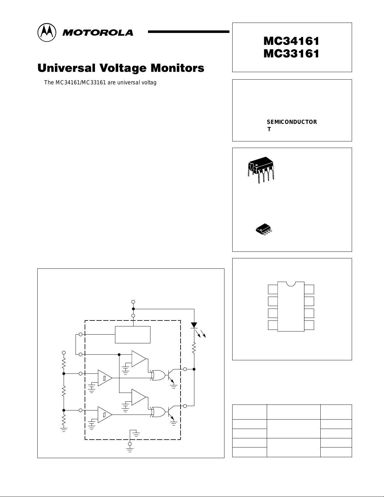
Simplified Block Diagram
(Positive Voltage Window Detector Application)
V
CC
8
1
V
S
7
2
3
+
–
+
1.27V
+
–
+
1.27V
2.54V
Reference
–
+
+
2.8V
–
+
+
0.6V
4
PIN CONNECTIONS
1
V
ref
2
Input 1
3
Input 2
4
Gnd
(TOP VIEW)
6
5
MC34161D
MC34161P Plastic DIP
MC33161D SO–8
MC33161P Plastic DIP
ORDERING INFORMATION
Operating
Device
Temperature Range
TA = 0° to +70°C
TA = –40° to +85°C
8
V
CC
7
Mode Select
6
Output 1
5
Output 2
Package
SO–8
MOTOROLA ANALOG IC DEVICE DATA
Motorola, Inc. 1998 Rev 1.1
1
MC34161 MC33161
MAXIMUM RATINGS
Rating Symbol Value Unit
Power Supply Input Voltage V
Comparator Input Voltage Range V
Comparator Output Sink Current (Pins 5 and 6) (Note 1) I
Comparator Output Voltage V
Power Dissipation and Thermal Characteristics (Note 1)
P Suffix, Plastic Package, Case 626
Maximum Power Dissipation @ TA = 70°C
Thermal Resistance, Junction–to–Air
D Suffix, Plastic Package, Case 751
Maximum Power Dissipation @ TA = 70°C
Thermal Resistance, Junction–to–Air
Operating Junction Temperature T
Operating Ambient Temperature (Note 3)
MC34161
MC33161
Storage Temperature Range T
Sink
P
R
P
R
CC
in
out
D
θJA
D
θJA
T
A
stg
J
ELECTRICAL CHARACTERISTICS (VCC = 5.0 V, for typical values TA = 25°C, for min/max values TA is the operating
ambient temperature range that applies [Notes 2 and 3], unless otherwise noted.)
Characteristics Symbol Min Typ Max Unit
COMPARATOR INPUTS
Threshold Voltage, Vin Increasing (TA = 25°C)
Threshold Voltage, Vin Increasing (TA = T
Threshold Voltage Variation (VCC = 2.0 V to 40 V) ∆V
Threshold Hysteresis, Vin Decreasing V
Threshold Difference |V
Reference to Threshold Difference (V
Input Bias Current (Vin = 1.0 V)
Input Bias Current (Vin = 1.5 V)
MODE SELECT INPUT
Mode Select Threshold Voltage (Figure 5) Channel 1
Mode Select Threshold Voltage (Figure 5) Channel 2
COMPARATOR OUTPUTS
Output Sink Saturation Voltage (I
Output Sink Saturation Voltage (I
Output Sink Saturation Voltage (I
Off–State Leakage Current (VOH = 40 V) I
REFERENCE OUTPUT
Output Voltage (IO = 0 mA, TA = 25°C) V
Load Regulation (IO = 0 mA to 2.0 mA) Reg
Line Regulation (VCC = 4.0 V to 40 V) Reg
Total Output Variation over Line, Load, and Temperature ∆V
Short Circuit Current I
TOTAL DEVICE
Power Supply Current (V
Power Supply Current (V
Operating Voltage Range (Positive Sensing)
Operating Voltage Range (Negative Sensing)
NOTES: 1. Maximum package power dissipation must be observed.
2.Low duty cycle pulse techniques are used during test to maintain junction temperature as close to ambient as possible.
3.T
=0°C for MC34161 T
low
–40°C for MC33161 +85°C for MC33161
– V
th1
Mode
Mode
| V
th2
ref
= 2.0 mA)
Sink
= 10 mA)
Sink
= 0.25 mA, VCC = 1.0 V)
Sink
, V
, V
in1
, Vin 1, Vin 2 = Gd) (VCC = 40 V)
to T
min
– V
), (V
in1
= Gnd) (VCC = 5.0 V)
in2
= +70°C for MC34161
high
max
ref
)
– V
) V
in2
40 V
– 1.0 to +40 V
20 mA
40 V
800
100
450
178
+150 °C
0 to +70
– 40 to +85
– 55 to +150 °C
V
V
V
th
th
H
D
RTD
I
IB
th(CH 1)
th(CH 2)
V
OL
OH
ref
load
line
ref
SC
I
CC
V
CC
mW
°C/W
mW
°C/W
°C
1.245
1.235
– 7.0 15 mV
15 25 35 mV
– 1.0 15 mV
1.20 1.27 1.32 V
–
–
V
+0.15
ref
0.3
–
–
–
– 0 1.0 µA
2.48 2.54 2.60 V
– 0.6 15 mV
– 5.0 15 mV
2.45 – 2.60 V
– 8.5 30 mA
–
–
2.0
4.0
1.27
–
40
85
V
+0.23
ref
0.63
0.05
0.22
0.02
450
560
–
–
V
1.295
1.295
200
400
+0.30
ref
0.9
0.3
0.6
0.2
700
900
40
40
V
nA
V
V
µA
V
2
MOTOROLA ANALOG IC DEVICE DATA
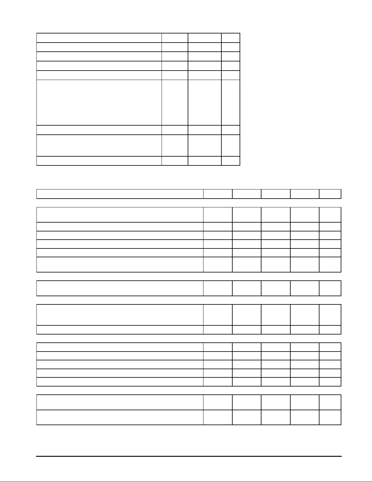
Figure 1. Comparator Input Threshold Voltage
6.0
VCC = 5.0 V
RL = 10 k to V
5.0
TA =
4.0
3.0
2.0
, OUTPUT VOL TAGE (V)
TA = 85°C
out
TA = 25°C
V
1.0
TA = –40°C
0
1.22 1.281.23 1.24 1.25 1.26 1.27 1.29
CC
25°C
TA = 85°C
TA = 25
TA = –40
Vin, INPUT VOLTAGE (V)
Figure 3. Output Propagation Delay Time
versus Percent Overdrive
3600
3000
2400
1800
1200
, OUTPUT PROP AGATION DELAY TIME (ns)
PHL
t
600
VCC = 5.0 V
°
C
TA = 25
1
4.0 6.00 2.0
PERCENT OVERDRIVE (%)
1. V
= Gnd, Output Falling
Mode
2. V
= VCC, Output Rising
Mode
3. V
= VCC, Output Falling
Mode
4. V
= Gnd, Output Rising
Mode
2
3
4
8.0 10
MC34161 MC33161
500
400
300
200
°
C
°
C
IB
100
I , INPUT BIAS CURRENT (nA)
0
0 4.0 5.0
Figure 4. Output V oltage versus Supply Voltage
8.0
6.0
4.0
, OUTPUT VOL TAGE (V)
out
2.0
V
0
0 2.0 4.0 6.0 8.0
Figure 2. Comparator Input Bias Current
versus Input V oltage
VCC = 5.0 V
V
= Gnd
Mode
°
C
TA = 25
1.0 3.02.0
Vin, INPUT VOLTAGE (V)
Undervoltage Detector
Programmed to trip at 4.5 V
R1 = 1.8 k, R2 = 4.7 k
RL = 10 k to V
Refer to Figure 16
CC
TA = –40°C
°
C
TA = –25
°
TA = –85
C
VCC, SUPPLY VOLTAGE (V)
Figure 5. Mode Select Thresholds
6.0
Channel 2 Threshold Channel 1 Threshold
5.0
VCC = 5.0 V
RL = 10 k to V
TA = 85°C
TA = 25°C
TA = –40°C
1.0 3.00 0.5 1.5 2.52.0 3.5
, MODE SELECT INPUT VOLTAGE (V)
CC
TA = –40°C
, CHANNEL OUTPUT VOLTAGE (V)
out
V
4.0
3.0
2.0
1.0
0
V
Mode
MOTOROLA ANALOG IC DEVICE DATA
°
TA = 85
TA = 25°C
Figure 6. Mode Select Input Current
versus Input V oltage
40
µ
VCC = 5.0 V
35
30
25
20
15
C
10
, MODE SELECT INPUT CURRENT ( A)
5.0
Mode
0
I
°
C
TA = 25
1.0 3.02.00 4.0 5.0
V
, MODE SELECT INPUT VOLTAGE (V)
Mode
3
MC34161 MC33161
2.8
2.4
2.0
1.6
1.2
0.8
ref
V , REFERENCE VOLTAGE (V)
0.4
0
0
0
–2.0
Figure 7. Reference V oltage
versus Supply V oltage
V
Mode
TA = 25
10 3020 40
VCC, SUPPLY VOLTAGE (V)
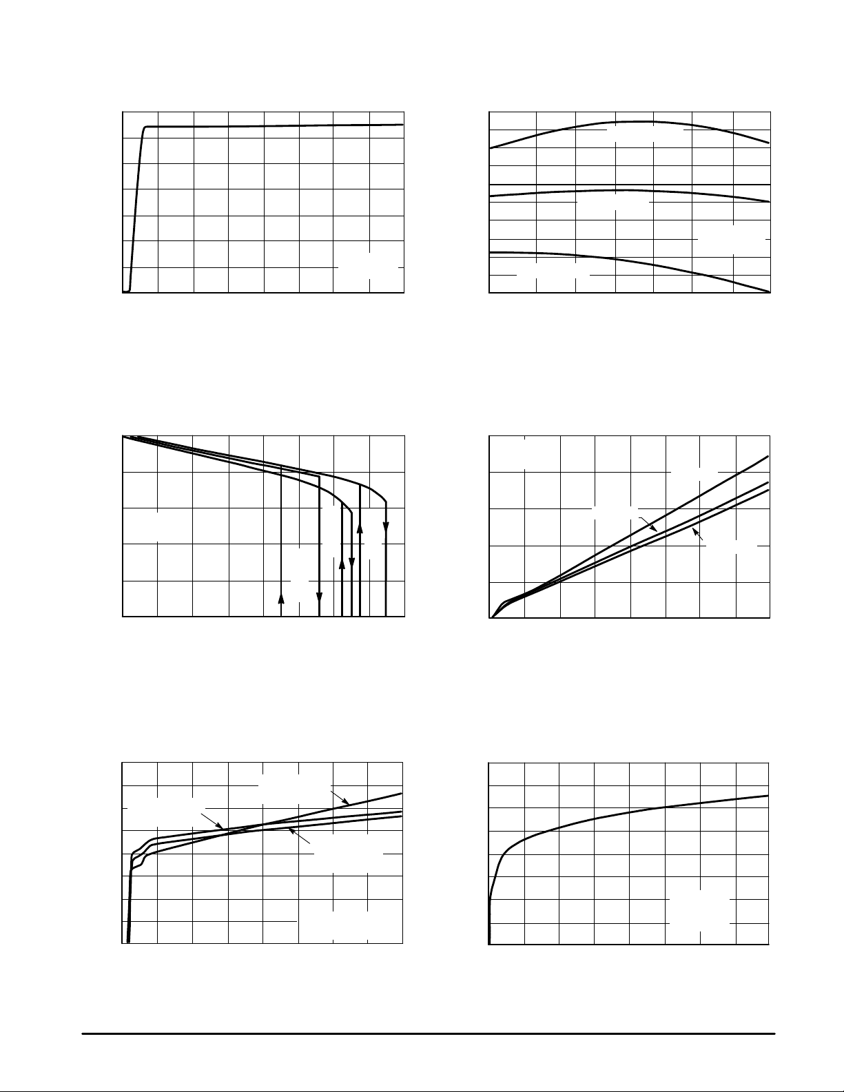
Figure 9. Reference V oltage Change
versus Source Current
= Gnd
°
C
Figure 8. Reference V oltage
versus Ambient T emperature
2.610
V
Max = 2.60 V
V
Typ = 2.54 V
ref
ref
VCC = 5.0 V
V
°C)
2.578
2.546
2.514
2.482
, REFERENCE OUTPUT VOLTAGE (V)
ref
V
2.450
V
Min = 2.48 V
ref
–55 –25 0 25 50 75 100 125
TA, AMBIENT TEMPERATURE (
Figure 10. Output Saturation Voltage
versus Output Sink Current
0.5
VCC = 5.0 V
V
= Gnd
Mode
0.4
TA = 85°C
Mode
= Gnd
–4.0
VCC = 5.0 V
V
= Gnd
Mode
–6.0
–8.0
, REFERENCE VOLTAGE CHANGE (mV)
ref
V
–10
1.00
I
ref
Figure 11. Supply Current versus
0.8
V
= Gnd
Mode
0.6
Pins 2, 3 = 1.5 V
0.4
, SUPPLY CURRENT (mA)
0.2
CC
I
0
C
°
= 85
T
C
°
= –40
A
T
2.0 3.0 4.0 5.0 6.0 7.0 8.0
, REFERENCE SOURCE CURRENT (mA)
C
°
= 25
A
A
T
Supply V oltage
V
= V
Mode
Pins 2, 3 = Gnd
100
VCC, SUPPLY VOLTAGE (V)
20 30 40
CC
V
= V
Mode
Pin 1 = 1.5 V
Pin 2 = Gnd
ICC measured at Pin 8
TA = 25
ref
°
C
0.3
0.2
0.1
, OUTPUT SA TURATION VOLTAGE (V)
out
V
1.6
1.2
0.8
, INPUT SUPPL Y CURRENT (mA)
0.4
CC
I
TA = 25°C
TA = –40°C
0
4.00
I
, OUTPUT SINK CURRENT (mA)
out
8.0 12 16
Figure 12. Supply Current
versus Output Sink Current
VCC = 5.0 V
V
= Gnd
Mode
°
C
TA = 25
0
4.00
I
, OUTPUT SINK CURRENT (mA)
out
8.0 12 16
4
MOTOROLA ANALOG IC DEVICE DATA
MC34161 MC33161
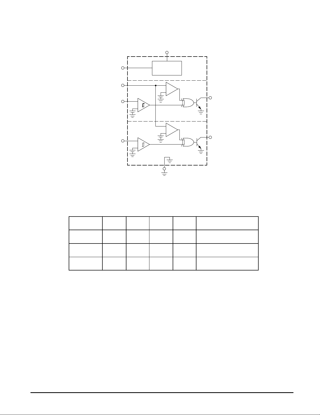
Figure 13. MC34161 Representative Block Diagram
V
CC
8
V
ref
Mode Select
Input 1
Input 2
2.54V
1
7
+
2
3
–
+
1.27V
+
–
+
1.27V
Reference
+
2.8V
+
0.6V
Gnd
–
+
–
+
4
Channel 1
Output 1
6
Channel 2
Output 2
5
Figure 14. Truth Table
Mode Select
Pin 7
GND 0
V
ref
VCC (>2.0 V) 0
Input 1
Pin 2
Output 1
Pin 6
1
0
1
1
0
1
0
1
1
0
Input 2
Pin 3
0
1
0
1
0
1
Output 2
Pin 5
0
1
1
0
1
0
Comments
Channels 1 & 2: Noninverting
Channel 1: Noninverting
Channel 2: Inverting
Channels 1 & 2: Inverting
MOTOROLA ANALOG IC DEVICE DATA
5
 Loading...