Motorola MC34156FN Datasheet

SEMICONDUCTOR
TECHNICAL DATA
28–CHANNEL
INKJET DRIVER
(SMARTMOS Technology)
Pin No.
1
2
3
4
5
6
7
8
9
10
11
12
13
14
15
16
17
18
19
20
21
22
23
24
25
26
27
28
29
30
31
32
33
34
35
36
37
38
39
40
41
42
43
44
Pin Name
IND
V
DD
Gnd
ENB
Chip Enable
OUTB0
OUTB1
OUTB2
OUTB3
OUTB4
OUTB5
OUTB6
OUTB7
OUTB8
OUTB9
Gnd
N/C
N/C
N/C
OUTB10
OUTB11
OUTB12
OUTB13
OUTA13
OUTA12
OUTA11
OUTA10
COM
Gnd
OUTA9
OUTA8
OUTA7
OUTA6
OUTA5
OUTA4
OUTA3
OUTA2
OUTA1
OUTA0
ENA
INA
Gnd
INB
INC
Pin Description
4th Decoder Input
Power Supply
Ground
Enable Pin for B Set Drivers
Chip Enable
B Set 1st Driver
B Set 2nd Driver
B Set 3rd Driver
B Set 4th Driver
B Set 5th Driver
B Set 6th Driver
B Set 7th Driver
B Set 8th Driver
B Set 9th Driver
B Set 10th Driver
Ground
Not Connected
Not Connected
Not Connected
B Set 11th Driver
B Set 12th Driver
B Set 13th Driver
B Set 14th Driver
A Set 14th Driver
A Set 13th Driver
A Set 12th Driver
A Set 11th Driver
Common
Ground
A Set 10th Driver
A Set 9th Driver
A Set 8th Driver
A Set 7th Driver
A Set 6th Driver
A Set 5th Driver
A Set 4th Driver
A Set 3rd Driver
A Set 2nd Driver
A Set 1st Driver
Enable Pin for A Set Drivers
1st Decoder Input
Ground
2nd Decoder Input
3rd Decoder Input
FN SUFFIX
PLASTIC PACKAGE
CASE 777
44
1
PIN ASSIGNMENTS
Order this document from Analog Marketing
1
MOTOROLA ANALOG IC DEVICE DATA
The MC34156 is a 28–Channel Decoder/Driver intended to be used in
inkjet printer applications. By using sophisticated SMARTMOS technology, it
has been possible to combine low power CMOS inputs and logic and high
current, high voltage bipolar outputs capable of sustaining a maximum of 30 V .
A 4–to–14 line decoder determines the selected output driver (n) in each
14–driver bank. Two independent output enable inputs (active low) then
provide the final decoding to activate 1– or 2–of–28 outputs (OUTAn and/or
OUTBn). The ac electrical characteristics of the drivers are tightly controlled
and thereby the energy of the device delivers to the inkjet print head. A Chip
Enable function is provided to lock out the drivers during system power up.
The 28 bipolar power outputs are open collector 30 V Darlington drivers
capable of sinking 500 mA at ambient temperatures up to 70°C. All driver
outputs are capable of withstanding a contact discharge of ±8.0 kV with the
IC biased.
• ESD Output Protection with Clamping Diodes
• Addressable Data Entry
• Tightly Controlled AC and Electrical Characteristics for Inkjet Printers
• CMOS, TTL Compatible Inputs
• Low Power CMOS Logic
SMARTMOS is a trademark of Motorola, Inc.
ORDERING INFORMATION
Device
Operating
Temperature Range
Package
MC34156FN TA = 0° to +70°C Plastic Package
Simplified Block Diagram
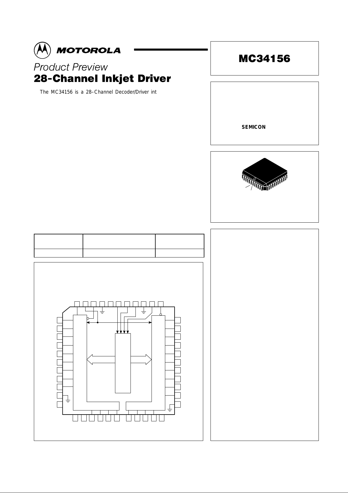
OUTB1 OUTA0
OUTB2 OUTA1
OUTB3 OUTA2
OUTB4 OUTA3
OUTB5 OUTA4
OUTB6 OUTA5
OUTB7 OUTA6
OUTB8 OUTA7
OUTB9 OUTA8
Gnd OUTA9
N/C Gnd
7
8
9
10
11
12
13
14
15
16
17
39
38
37
36
35
34
33
32
31
30
29
6
5
4
3
2
1
44
43
42
41
40
18
19
20
21
22
23
24
25
26
27
28
OUTB0
N/C
Chip Enable
Output Enable B
Gnd
Logic Supply
IND (MSB)
INC
INB
Gnd
INA (LSB)
Output Enable A
N/C
OUTB10
OUTB11
OUTB12
OUTB13
OUTA13
OUTA12
OUTA11
OUTA10
COM
Output Driver Bank B
4–T o–14 Line Decoder
Output Driver Bank A
V
DD
This document contains information on a product under development. Motorola reserves the
right to change or discontinue this product without notice.
Motorola, Inc. 1996 Issue 0

MC34156
2
MOTOROLA ANALOG IC DEVICE DATA
OUTA0
OUTA1
OUTA2
OUTA13
OUTB0
OUTB1
OUTB2
OUTB13
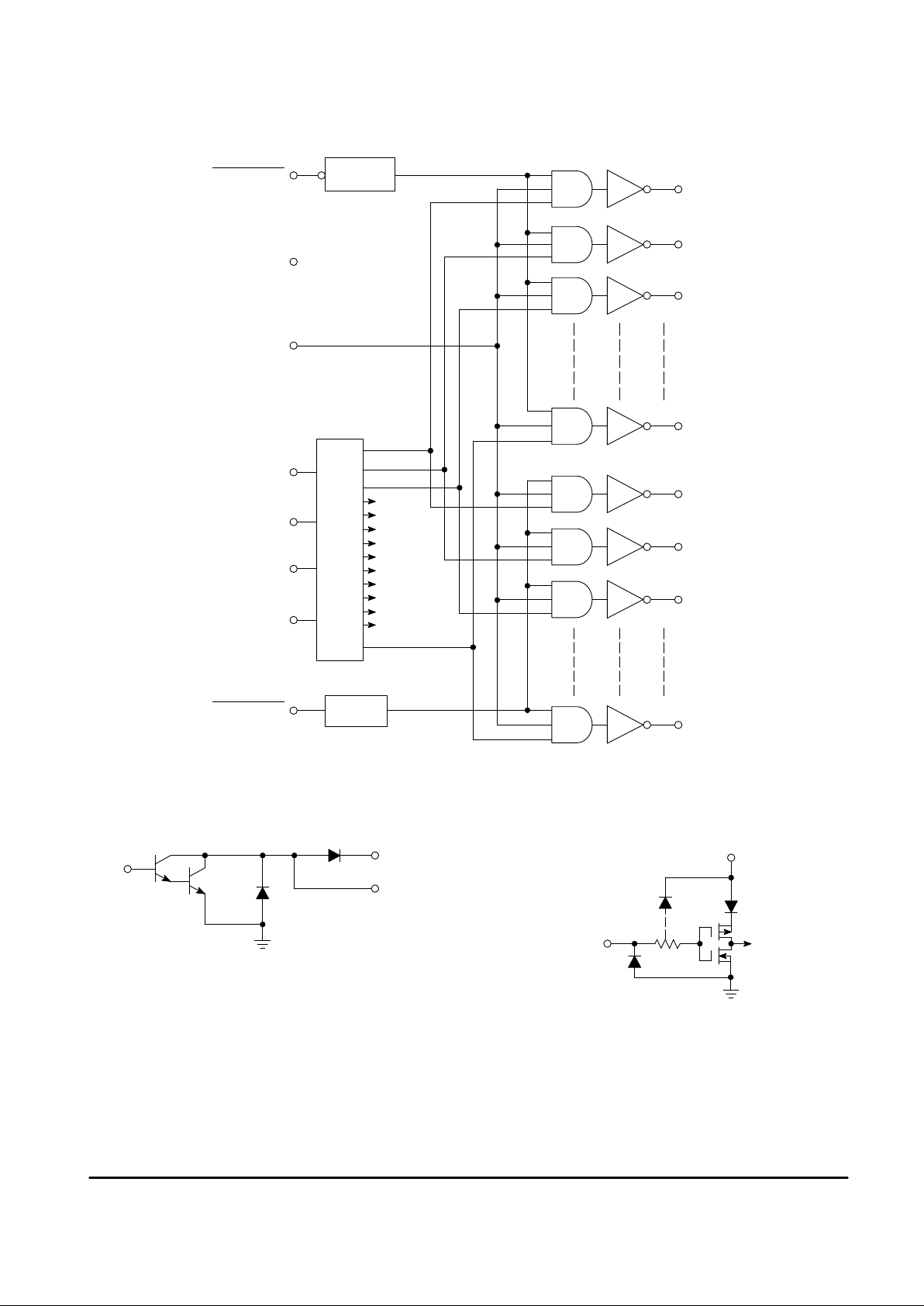
Output Enable A
Logic Supply
Chip Enable
INA (LSB)
INB
INC
IND (MSB)
Output Enable B
Turn Off
Delay
Turn On
Delay
4–to–14 Line Decoder
Figure 1. Functional Block Diagram
Figure 2. Output Driver Configuration Figure 3. Typical Input Circuit
COM
OUT
V
DD
IN
 Loading...