

Motorola MC34115DW, MC34115P Datasheet
Device
Operating
Temperature Range
Package
SEMICONDUCTOR
TECHNICAL DATA
CONTINUOUSLY VARIABLE
SLOPE DELTA
MODULATOR/DEMODULATOR
ORDERING INFORMATION
MC34115P
MC34115DW
TA = 0° to +70°C
Plastic DIP
SO–16L
P SUFFIX
PLASTIC PACKAGE
CASE 648
1 16
15
14
13
12
11
10
9
2
3
4
5
6
7
8
(Top View)
Analog Input (–)
Analog Feedback (+)
Syllabic Filter
Filter Input (–)
Analog Output
V
EE
V
CC
Digital Data Input (–)
Digital Output
PIN CONNECTIONS
Order this document by MC34115/D
DW SUFFIX
PLASTIC PACKAGE
CASE 751G
(SO–16L)
Gain Control
Ref Input (+)
VCC/2 Output
Coincidence
Output
Digital Threshold
Clock
Encode/Decode
16
1
1
16
1
MOTOROLA ANALOG IC DEVICE DATA
Providing a simplified approach to digital speech encoding/decoding, the
MC34115 CVSD is designed for speech synthesis and commercial telephone
applications. A single IC provides both encoding and decoding functions.
• Encode and Decode Functions Selectable with a Digital Input
• Utilization of Compatible I
2
L – Linear Bipolar Technology
• CMOS Compatible Digital Output
• Digital Input Threshold Selectable (V
CC
/2 Reference Provided On–Chip)
• 3–Bit Algorithm
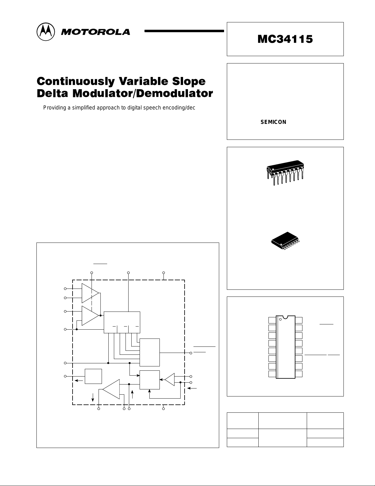
CVSD Block Diagram
This device contains 144 active transistors.
Syllabic Filter
Coincidence
Output
Encode/Decode
Analog Input
Analog
Feedback
Digital
Data Input
Digital
Threshold
Digital Output
VCC/2 Output
Clock
3–Bit
Shift Register
Integrator
Amplifier
Analog
Output
Ref
Input
(+)
VCC/2
Ref
Filter
Input
(–)
I
O
I
Int
Logic
Slope
Polarity
Switch
V/I
Converter
Gain Control
I
GC
V
th
1
2
13
12
9
10
7 5 6
15 14
11
3
4
+
–
Q Q Q Q Q Q
+
–
+
–
8
I
Ref
V
CC
16
V
EE
Motorola, Inc. 1996 Rev 1
MC34115
2
MOTOROLA ANALOG IC DEVICE DATA
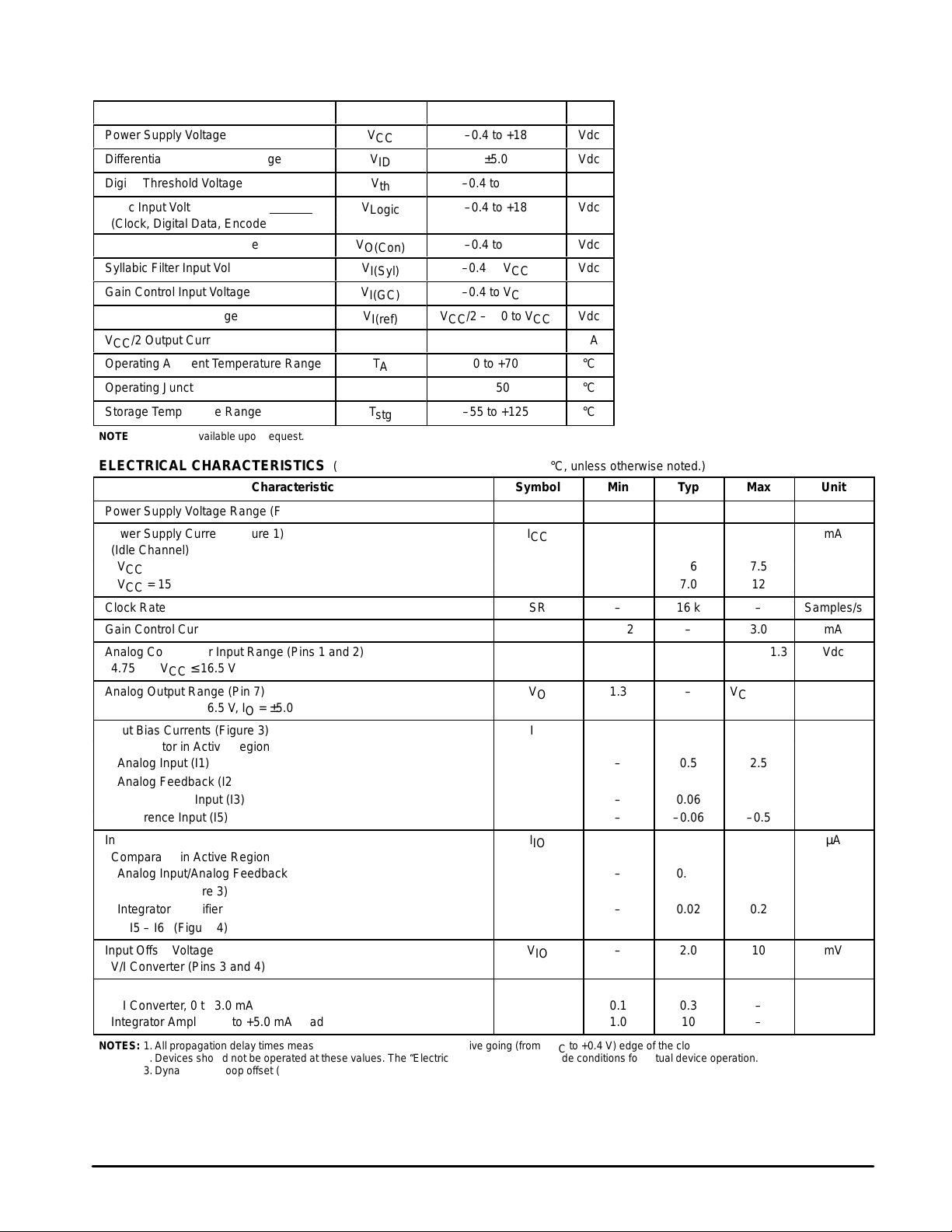
MAXIMUM RATINGS (All voltages referenced to V
EE
, TA = 25°C,
unless otherwise noted.) (Note 2)
Rating
Symbol Value Unit
Power Supply Voltage
ÁÁÁÁ
ÁÁÁÁ
ÁÁÁÁ
V
CC
–0.4 to +18
Vdc
Differential Analog Input Voltage
ÁÁÁÁ
ÁÁÁÁ
ÁÁÁÁ
V
ID
±5.0
Vdc
Digital Threshold Voltage
ÁÁÁÁ
ÁÁÁÁ
ÁÁÁÁ
V
th
–0.4 to V
CC
Vdc
Logic Input Voltage
ÁÁÁÁ
ÁÁÁÁ
ÁÁÁÁ
V
Logic
–0.4 to +18
Vdc
(Clock, Digital Data, Encode/Decode)
ÁÁÁÁ
ÁÁÁÁ
Coincidence Output Voltage
ÁÁÁÁ
ÁÁÁÁ
ÁÁÁÁ
V
O(Con)
–0.4 to +18
Vdc
Syllabic Filter Input Voltage
ÁÁÁÁ
ÁÁÁÁ
ÁÁÁÁ
V
I(Syl)
–0.4 to V
CC
Vdc
Gain Control Input Voltage
ÁÁÁÁ
ÁÁÁÁ
ÁÁÁÁ
V
I(GC)
–0.4 to V
CC
Vdc
Reference Input Voltage
ÁÁÁÁ
ÁÁÁÁ
ÁÁÁÁ
V
I(ref)
VCC/2 – 1.0 to V
CC
Vdc
VCC/2 Output Current
ÁÁÁÁ
ÁÁÁÁ
ÁÁÁÁ
I
ref
–25
mA
Operating Ambient Temperature Range
ÁÁÁÁ
ÁÁÁÁ
ÁÁÁÁ
T
A
0 to +70
°C
Operating Junction Temperature
ÁÁÁÁ
ÁÁÁÁ
ÁÁÁÁ
T
J
+150
°C
Storage Temperature Range
ÁÁÁÁ
ÁÁÁÁ
ÁÁÁÁ
T
stg
–55 to +125
°C
NOTE: ESD data available upon request.
ELECTRICAL CHARACTERISTICS (V
CC
= 12 V, VEE = Gnd, TA = 0° to 70°C, unless otherwise noted.)
Characteristic
Symbol Min Typ Max Unit
Power Supply Voltage Range (Figure 1) V
CC
4.75 12 16.5 Vdc
Power Supply Current (Figure 1) I
CC
mA
(Idle Channel)
VCC = 5.0 V – 4.6 7.5
VCC = 15 V – 7.0 12
Clock Rate SR – 16 k – Samples/s
Gain Control Current Range (Figure 2) I
GCR
0.002 – 3.0 mA
Analog Comparator Input Range (Pins 1 and 2) V
I
1.3 – VCC – 1.3 Vdc
4.75 V ≤ VCC ≤ 16.5 V
Analog Output Range (Pin 7) V
O
1.3 – VCC – 1.3 Vdc
4.75 V ≤ VCC ≤ 16.5 V, IO = ±5.0 mA
Input Bias Currents (Figure 3) I
IB
µA
Comparator in Active Region
Analog Input (I1) – 0.5 2.5
Analog Feedback (I2) – 0.5 2.5
Syllabic Filter Input (I3) – 0.06 0.5
Reference Input (I5) – –0.06 –0.5
Input Offset Current I
IO
µA
Comparator in Active Region
Analog Input/Analog Feedback – 0.15 0.8
I1 – I2 (Figure 3)
Integrator Amplifier – 0.02 0.2
I5 – I6 (Figure 4)
Input Offset Voltage V
IO
– 2.0 10 mV
V/I Converter (Pins 3 and 4) (Figure 5)
Transconductance gm mA/mV
V/I Converter, 0 to 3.0 mA 0.1 0.3 –
Integrator Amplifier, 0 to +5.0 mA Load 1.0 10 –
NOTES: 1. All propagation delay times measured 50% to 50% from the negative going (from VCC to +0.4 V) edge of the clock.
2.Devices should not be operated at these values. The “Electrical Characteristics” provide conditions for actual device operation.
3.Dynamic total loop offset (ΣV
offset
) equals VIO (comparator) (Figure 3) minus V
IOX
(Figure 5). The input offset voltages of the analog
comparator and of the integrator amplifier include the effects of input offset current through the input resistors. The slope polarity switch
current mismatch appears as an average voltage across the 10 k integrator resistor. The clock frequency is 16 kHz. Idle channel
performance is guaranteed if this dynamic total loop offset is less than one–half of the change in integrator output voltage during one
clock cycle (ramp step size).
MC34115
3
MOTOROLA ANALOG IC DEVICE DATA
ELECTRICAL CHARACTERISTICS (continued) (V
CC
= 12 V, VEE = Gnd, TA = 0° to 70°C, unless otherwise noted.)
Characteristic UnitMaxTypMinSymbol
Propagation Delay Times (Note 1) µs
Clock Trigger to Digital Output t
PLH
– 1.0 3.0
CL = 25 pF to Gnd t
PHL
– 0.8 3.0
Clock Trigger to Coincidence Output t
PLH
– 1.0 3.5
CL = 25 pF to Gnd, RL = 4.0 kΩ to V
CC
t
PHL
– 0.8 2.5
Coincidence Output Voltage – Low Logic Stage (I
OL(Con)
= 3.0 mA) V
OL(Con)
– 0.12 0.25 Vdc
Coincidence Output Leakage Current – High Logic State (VOH = 15 V) I
OH(Con)
– 0.01 0.5 µA
Applied Digital Threshold Voltage Range (Pin 12) V
th
1.2 – VCC – 2.0 Vdc
Digital Threshold Input Current I
I(th)
µA
1.2 V ≤ Vth ≤ VCC – 2.0 V
VIL Applied to Pins 13, 14 and 15 – – 5.0
VIH Applied to Pins 13, 14 and 15 – –10 –50
Maximum Integrator Amplifier Output Current I
O
±5.0 – – mA
VCC/2 Generator Maximum Output Current (Source Only) I
ref
–10 – – mA
VCC/2 Generator Output Impedance (0 to –10 mA) z
ref
– 3.0 6.0 Ω
VCC/2 Generator Tolerance (4.75 V ≤ VCC ≤ 16.5 V) εr – – ±3.5 %
Logic Input Voltage (Pins 13, 14 and 15) Vdc
Low Logic State V
IL
V
EE
– Vth – 0.4
High Logic State V
IH
Vth + 0.4 – 16.5
Dynamic Total Loop Offset Voltage (Note 3) (Figures 3, 4 and 5) ΣV
offset
mV
IGC = 33 µA, VCC = 12 V
TA = 25°C – ±2.5 ±7.0
0°C ≤ TA ≤ +70°C – ±3.0 ±10
IGC = 33 µA, VCC = 5.0 V
TA = 25°C – ±4.0 ±8.0
0°C ≤ TA ≤ +70°C – ±4.5 ±12
Digital Output Voltage (Pin 9) Vdc
IOL = 3.6 mA V
OL
– 0.1 0.4
IOH = –0.35 mA V
OH
VCC – 1.0 VCC – 0.2 –
Syllabic Filter Applied Voltage (Pin 3) (Figure 2) V
I(Syl)
3.2 – V
CC
Vdc
Integrating Current (Figure 2) I
Int
IGC = 12 µA 8.0 10 12 µA
IGC = 1.5 mA 1.4 1.5 1.6 mA
IGC = 3.0 mA 2.75 3.0 3.25 mA
Dynamic Integrating Current Match (Figure 6) (IGC = 1.5 mA) V
O(Ave)
– ±100 ±300 mV
Input Current – High Logic State (VIH = 16.5 V) I
IH
µA
Digital Data Input – – 5.0
Clock Input – – 5.0
Encode/Decode Input – – 5.0
Input Current – Low Logic State (VIL = 0 V) I
IL
µA
Digital Data Input –10 – –
Clock Input –360 – –
Encode/Decode Input –36 – –
Clock Input, VIL = 0.4 V –72 – –
NOTES: 1. All propagation delay times measured 50% to 50% from the negative going (from VCC to +0.4 V) edge of the clock.
2.Devices should not be operated at these values. The “Electrical Characteristics” provide conditions for actual device operation.
3.Dynamic total loop offset (ΣV
offset
) equals VIO (comparator) (Figure 3) minus V
IOX
(Figure 5). The input offset voltages of the analog
comparator and of the integrator amplifier include the effects of input offset current through the input resistors. The slope polarity switch
current mismatch appears as an average voltage across the 10 k integrator resistor. The clock frequency is 16 kHz. Idle channel
performance is guaranteed if this dynamic total loop offset is less than one–half of the change in integrator output voltage during one
clock cycle (ramp step size).

MC34115
4
MOTOROLA ANALOG IC DEVICE DATA
DEFINITION AND FUNCTION OF PINS
Pin 1 – Analog Input
This is the analog comparator inverting input where the
voice signal is applied. It may be ac or dc coupled depending
on the application. If the voice signal is to be level shifted to
the internal reference voltage, then a bias resistor between
Pins 1 and 10 is used. The resistor is used to establish the
reference as the new dc average of the ac coupled signal.
The analog comparator was designed for low hysteresis
(typically less than 0.1 mV) and high gain (typically 70 dB).
Pin 2 – Analog Feedback
This is the noninverting input to the analog signal
comparator. In an encoder application it should be
connected to the analog output of the encoder circuit. This
may be Pin 7 or a low pass filter output connected to Pin 7.
In a decode circuit, Pin 2 is not used and may be tied to
VCC/2 at Pin 10 or ground.
The analog input comparator has bias currents of 2.5 µA
max, thus the driving impedances of Pins 1 and 2 should be
equal to avoid disturbing the idle channel characteristics of
the encoder.
Pin 3 – Syllabic Filter
This is the point at which the syllabic filter voltage is
returned to the IC in order to control the integrator step size.
It is an NPN input to an op amp. The syllabic filter consists of
an RC network between Pins 1 1 and 3. Typical time constant
values of 6.0 ms to 50 ms are used in voice codecs.
Pin 4 – Gain Control Input
The syllabic filter voltage appears across CS of the syllabic
filter and is the voltage between VCC and Pin 3. The active
voltage to current (V–I) converter drives Pin 4 to the same
voltage at a slew rate of typically 0.5 V/µs. Thus the current
injected into Pin 4 (IGC) is the syllabic filter voltage divided by
the Rx resistance. Figure 7 shows the relationship between
IGC (x–axis) and the integrating current, I
Int
(y–axis). The
discrepancy, which is most significant at very low currents, is
due to circuitry within the slope polarity switch which enables
trimming to a low total loop offset. The Rx resistor is then
varied to adjust the loop gain of the codec, but should be no
larger than 5.0 kΩ to maintain stability.
Pin 5 – Reference Input
This pin is the noninverting input of the integrator amplifier.
It is used to reference the dc level of the output signal. In an
encoder circuit, it must reference the same voltage as Pin 1
and is tied to Pin 10.
Pin 6 – Filter Input
This inverting op amp input is used to connect the
integrator external components. The integrating current (I
Int
)
flows into Pin 6 when the analog input (Pin 1) is high with
respect to the analog feedback (Pin 2) in the encode mode
or when the digital data input (Pin 13) is high in the decode
mode. For the opposite states, I
Int
flows out of Pin 6. Single
integration systems require a capacitor and resistor between
Pins 6 and 7. Multipole configurations will have different
circuitry. The resistance between Pins 6 and 7 should
typically be between 8.0 kΩ and 13 kΩ to maintain good idle
channel characteristics.
Pin 7 – Analog Output
This is the integrator op amp output. It is capable of driving
a 600 Ω load referenced to VCC/2 to +6.0 dBm and can
otherwise be treated as an op amp output. Pins 5, 6 and 7
provide full access to the integrator op amp for designing
integration filter networks. The slew rate of the internally
compensated integrator op amp is typically 0.5 V/µs. Pin 7
output is current limited for both polarities of current flow at
typically 30 mA.
Pin 8 – V
EE
The circuit is designed to work in either single or dual
power supply applications. Pin 8 is always connected to the
most negative supply.
Pin 9 – Digital Output
The digital output provides the results of the delta
modulator’s conversion. It swings between VCC and VEE and
is CMOS or TTL compatible. Pin 9 is inverting with respect to
Pin 1 and noninverting with respect to Pin 2. It is clocked on
the falling edge of Pin 14. The typical 10% to 90% rise and fall
times are 250 ns and 50 ns respectively for VCC = 12 V and
CL = 25 pF to ground.
Pin 10 – VCC/2 Output
An internal low impedance mid–supply reference is
provided for use in single supply applications. The internal
regulator is a current source and must be loaded with a
resistor to ensure its sinking capability. If a +6.0 dBmo signal
is expected across a 600 Ω input bias resistor, then Pin 10
must sink 2.2 V/600 Ω = 3.66 mA. This is possible only if
Pin 10 sources 3.66 mA into a resistor normally and will
source the difference under peak load. The reference load
resistor is chosen accordingly. A 0.1 µF bypass capacitor
from Pin 10 to VEE is also recommended. The VCC/2
reference is capable of sourcing 10 mA and can be used as
a reference elsewhere in the system circuitry.
Pin 11 – Coincidence
Output
The coincidence output will be low whenever the content
of the internal 3–bit shift register is all 1s or all 0s. Pin 11 is
an open collector NPN device and requires a pull–up
resistor. If the syllabic filter is to have equal charge and
discharge time constants, the value of RP should be much
less than RS. In systems requiring different charge and
discharge constants, the charging constant is RSCS while
the decay constant is (RS + RP)CS. Thus, longer decays are
easily achievable. The NPN device should not be required to
sink more than 3.0 mA. The typical 10% to 90% rise and fall
times are 200 ns and 100 ns respectively for RL = 4.0 kΩ to
12 V and CL = 25 pF to ground.
Pin 12 – Digital Threshold
This input sets the switching threshold for Pins 13, 14 and
15. It is intended to aid in interfacing different logic families
without external parts. Typically it is connected to the VCC/2
reference for CMOS interface or can be biased two diode
drops above VEE for TTL interface.
MC34115
5
MOTOROLA ANALOG IC DEVICE DATA
Pin 13 – Digital Data Input
In a decode application, the digital data stream is applied
to Pin 13. In an encoder it may be unused or may be used to
transmit a signaling message under the control of Pin 15. It is
an inverting input with respect to Pin 9. When Pins 9 and 13
are connected, a toggle flip–flop is formed and a forced idle
channel pattern can be transmitted. The digital data input
level should be maintained for 0.5 µs before and after the
clock trigger for proper clocking.
Pin 14 – Clock Input
The clock input determines the data rate of the codec
circuit. A 16 k bit rate requires a 16 kHz clock. The switching
threshold of the clock input is set by Pin 12. The shift register
circuit toggles on the falling edge of the clock input. The
minimum high time for the clock input is 300 ns and minimum
low time is 900 ns.
Pin 15 – Encode/Decode
This pin controls the connection of the analog input
comparator and the digital input comparator to the internal
shift register. If high, the result of the analog comparison will
be clocked into the register on the falling edge at Pin 14. If low,
the digital input state will be entered. This allows use of the IC
as an encoder/decoder or simplex codec without external
parts. Furthermore, it allows non–voice patterns to be forced
onto the transmission line through Pin 13 in an encoder.
Pin 16 – V
CC
The power supply range is from 4.75 to 16.5 V between
Pin VCC and VEE.
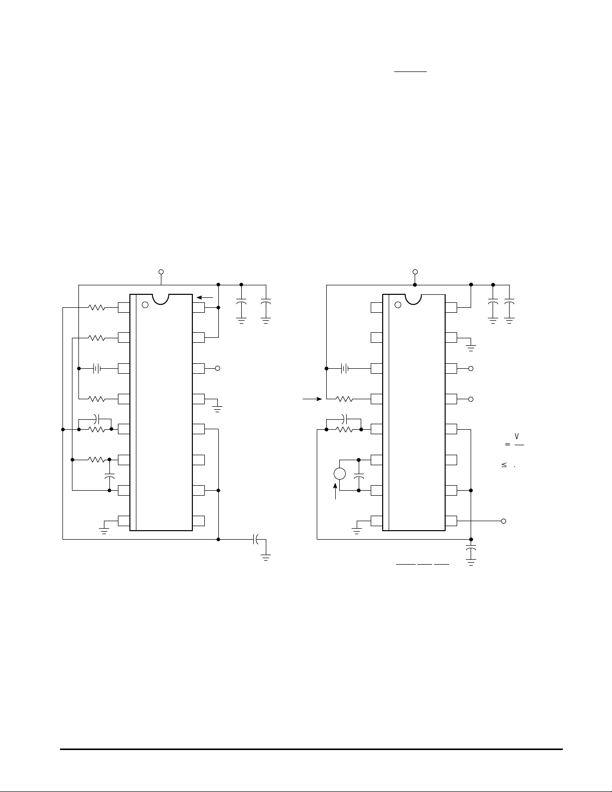
Figure 1. Power Supply Current
60 mV
10 k
0.05
0.1
Clock
I
CC
CVSD
MC34115
1.0 k
1.0 k
5.0 k
+ –
V
CC
10 k
0.05
0.1
Clock
(Note 2)
0.1
I
GC
CVSD
MC34115
V
B
R
x
Digital
Output
(Note 1)
Digital Data
Input
I
Int
A
+ –
NOTES: 1. Digital Output = Digital Data Input
2.For static testing, the clock is only necessary for
preconditioning to obtain proper state for a given input.
Figure 2. I
GCR
– Gain Control Range and I
Int
–
Integrating Current
IGC+
V
B
R
x
11
9
7
6
8
5
4
1
2
3
13
12
10
16
15
14
11
7
6
8
5
4
1
2
3
13
12
10
16
15
14
9
Rxv
5.0 k
10 µF 10 µF 0.1
V
CC
0.1
10 k
0.1
 Loading...