

Motorola MC34065P, MC34065DW, MC33065P, MC33065DW Datasheet
Order this document by MC34065/D
The MC34065 is a high performance, fixed frequency , dual current mode
controllers. It is specifically designed for off–line and dc–to–dc converter
applications offering the designer a cost effective solution with minimal
external components. This integrated circuit feature a unique oscillator for
precise duty cycle limit and frequency control, a temperature compensated
reference, two high gain error amplifiers, two current sensing comparators,
Drive Output 2 Enable pin, and two high current totem pole outputs ideally
suited for driving power MOSFETs.
Also included are protective features consisting of input and reference
undervoltage lockouts each with hysteresis, cycle–by–cycle current limiting,
and a latch for single pulse metering of each output.
The MC34065 and MC33065 are available in dual–in–line and surface
mount packages.
• Unique Oscillator for Precise Duty Cycle Limit and Frequency Control
• Current Mode Operation to 500 kHz
• Automatic Feed Forward Compensation
• Separate Latching PWMs for Cycle–By–Cycle Current Limiting
• Internally Trimmed Reference with Undervoltage Lockout
• Drive Output 2 Enable Pin
• Two High Current Totem Pole Outputs
• Input Undervoltage Lockout with Hysteresis
• Low Startup and Operating Current
HIGH PERFORMANCE
DUAL CHANNEL CURRENT
MODE CONTROLLER
SEMICONDUCTOR
TECHNICAL DATA
P SUFFIX
PLASTIC PACKAGE
CASE 648
DW SUFFIX
PLASTIC PACKAGE
CASE 751G
(SO–16L)
16
1
16
1
Representative Block Diagram
V
ref
Lockout
5.0 V
Reference
V
ref
Sync Input
R
T
C
T
Voltage
Feedback 1
Compensation 1
Drive Output 2
Enable
Voltage
Feedback 2
Compensation 2
15
1
3
2
4
5
14
13
12
R
R
Undervoltage
Oscillator
+
–
Error
Amp 1
+
–
Error
Amp 2
Gnd 8 Drive Gnd 9
This device contains 208 active transistors.
MOTOROLA ANALOG IC DEVICE DATA
V
CC
Undervoltage
Lockout
Latching
PWM 1
Latching
PWM 2
PIN CONNECTIONS
V
16
CC
Drive
Output 1
7
Current
Sense 1
6
Drive
Output 2
10
Current
Sense 2
11
Motorola, Inc. 1996 Rev 1
Sync Input
Voltage Feedback 1
Compensation 1
Current Sense 1
Drive Output 1
ORDERING INFORMATION
Device
MC34065DW
MC34065P
MC33065DW
MC33065P
1
2
C
T
3
R
T
4
5
6
7
89
Gnd
(Top View)
Operating
Temperature Range
TA = 0° to +70°C
TA = –40° to +85°C
16
V
CC
15
V
ref
Drive Output 2
14
Enable
13
Voltage Feedback 2
12
Compensation 2
11
Current Sense 2
10
Drive Output 2
Drive Gnd
Package
SO–16L
Plastic DIP
SO–16L
Plastic DIP
1
MC34065 MC33065
MAXIMUM RATINGS
Rating Symbol Value Unit
Total Power Supply and Zener Current (ICC + IZ) 50 mA
Output Current, Source or Sink (Note 1) I
O
Output Energy (Capacitive Load per Cycle) W 5.0 µJ
Current Sense, Enable, and Voltage Feedback Inputs V
in
Sync Input
High State (Voltage) V
Low State (Reverse Current) I
Error Amp Output Sink Current I
IH
IL
O
Power Dissipation and Thermal Characteristics
DW Suffix, Plastic Package Case 751G
Maximum Power Dissipation @ TA = 25°C P
Thermal Resistance, Junction–to–Air R
D
θJA
P Suffix, Plastic Package Case 648
Maximum Power Dissipation @ TA = 25°C P
Thermal Resistance, Junction–to–Air R
Operating Junction Temperature T
Operating Ambient Temperature T
D
θJA
J
A
MC34065 0 to +70
MC33065 –40 to +85
Storage Temperature Range T
NOTE: ESD data available upon request.
stg
1.0 A
–0.3 to +5.5 V
5.5 V
–5.0 mA
10 mA
862 mW
145 °C/W
1.25 W
100 °C/W
+150 °C
–65 to +150 °C
°C
ELECTRICAL CHARACTERISTICS (V
= 15 V [Note 2], RT = 8.2 kΩ, CT = 3.3 nF, for typical values TA = 25°C, for
CC
min/max values TA is the operating ambient temperature range that applies [Note 3].)
Characteristics
Symbol Min Typ Max Unit
REFERENCE SECTION
Reference Output Voltage (IO = 1.0 mA, TJ = 25°C) V
Line Regulation (VCC = 11 V to 15 V) Reg
Load Regulation (IO = 1.0 mA to 10 mA) Reg
Total Output Variation over Line, Load, and Temperature V
Output Short Circuit Current I
ref
line
load
ref
SC
4.9 5.0 5.1 V
– 2.0 20 mV
– 3.0 25 mV
4.85 – 5.15 V
30 100 – mA
OSCILLATOR AND PWM SECTIONS
Total Frequency Variation over Line and Temperature f
VCC = 11 V to 15 V, TA = T
low
to T
high
osc
MC34065 46.5 49 51.5
MC33065 45 49 53
Frequency Change with Voltage (VCC = 11 V to 15 V) ∆f
/∆V – 0.2 1.0 %
osc
Duty Cycle at each Output %
Maximum DC
Minimum DC
max
min
46 49.5 52
– – 0
Sync Input Current µA
High State (Vin = 2.4 V) I
Low State (Vin = 0.8 V) I
NOTES: 1. Maximum package power dissipation limits must be observed.
2.Adjust VCC above the startup threshold before setting to 15 V.
3.Low duty cycle pulse techniques are used during test to maintain junction temperature as close to ambient as possible:
T
= 0°C for the MC34065 T
low
T
= –40°C for the MC33065 T
low
4.This parameter is measured at the latch trip point with VFB = 0 V
5.Comparator gain is defined as
AV
+
= +70°C for MC34065
high
= +85°C for MC33065
high
D
V Compensation
D
V Current Sense
IH
IL
– 170 250
– 80 160
kHz
2
MOTOROLA ANALOG IC DEVICE DATA
MC34065 MC33065
ELECTRICAL CHARACTERISTICS (continued) (V
= 15 V [Note 2], RT = 8.2 kΩ, CT = 3.3 nF, for typical values TA = 25°C, for
CC
min/max values TA is the operating ambient temperature range that applies [Note 3].)
Characteristics UnitMaxTypMinSymbol
ERROR AMPLIFIERS
Voltage Feedback Input (VO = 2.5 V) V
Input Bias Current (VFB = 5.0 V) I
Open Loop Voltage Gain (VO = 2.0 to 4.0 V) A
FB
IB
VOL
2.42 2.5 2.58 V
– – 0.1 –1.0 µA
65 100 – dB
Unity Gain Bandwidth (TJ = 25°C) BW 0.7 1.0 – MHz
Power Supply Rejection Ratio (VCC = 11 V to 15 V) PSRR 60 90 – dB
Output Current mA
Source (VO = 3.0 V, VFB = 2.3 V) I
Sink (VO = 1.2 V, VFB = 2.7 V) I
source
sink
–0.45 –1.0 –
2.0 12 –
Output Voltage Swing V
High State (RL = 15 k to ground, VFB = 2.3 V) V
Low State (RL = 15 k to V
, VFB = 2.7 V) V
ref
OH
OL
5.0 6.2 –
– 0.8 1.1
CURRENT SENSE SECTION
Current Sense Input Voltage Gain (Notes 4 and 5) A
Maximum Current Sense Input Threshold (Note 4) V
Input Bias Current I
Propagation Delay (Current Sense Input to Output) t
PLN(In/Out)
V
th
IB
2.75 3.0 3.25 V/V
430 480 530 mV
– –2.0 –10 µA
– 150 300 ns
DRIVE OUTPUT 2 ENABLE PIN
Enable Pin Voltage V
High State (Output 2 Enabled) V
Low State (Output 2 Disabled) V
Low State Input Current (VIL = 0 V) I
IH
IL
IB
3.5 – V
ref
0 – 1.5
100 250 400 µA
DRIVE OUTPUTS
Output Voltage V
Low State (I
High State(I
Output Voltage with UVLO Activated (VCC = 6.0 V, I
Output Voltage Rise T ime (CL = 1.0 nF) t
Output Voltage Fall T ime (CL = 1.0 nF) t
= 20 mA) V
sink
(I
= 200 mA) – 1.6 2.5
sink
= 20 mA) V
source
(I
= 200 mA) 12 13.4 –
source
= 1.0 mA) V
sink
OL
OH
OL(UVLO)
r
f
– 0.1 0.4
13 13.5 –
– 0.1 1.1 V
– 28 150 ns
– 25 150 ns
UNDERVOLTAGE LOCKOUT SECTION
Startup Threshold V
Minimum Operating Voltage After Turn–On V
CC(min)
th
13 14 15 V
9.0 10 11 V
TOTAL DEVICE
Power Supply Current I
CC
Startup (VCC = 12 V) – 0.6 1.0
Operating (Note 2) – 20 25
Power Supply Zener Voltage (ICC = 30 mA) V
NOTES: 1. Maximum package power dissipation limits must be observed.
2.Adjust VCC above the startup threshold before setting to 15 V.
3.Low duty cycle pulse techniques are used during test to maintain junction temperature as close to ambient as possible:
T
= 0°C for the MC34065 T
low
T
= –40°C for the MC33065 T
low
4.This parameter is measured at the latch trip point with VFB = 0 V
5.Comparator gain is defined as
AV
+
= +70°C for MC34065
high
= +85°C for MC33065
high
D
V Compensation
D
V Current Sense
Z
15.5 17 19 V
mA
MOTOROLA ANALOG IC DEVICE DATA
3
MC34065 MC33065
PIN FUNCTION DESCRIPTION
Pin Function Description
1 Sync Input A narrow rectangular waveform applied to this input will synchronize the oscillator. A dc voltage
2 C
3 R
T
T
4 Voltage Feedback 1 This pin is the inverting input of Error Amplifier 1. It is normally connected to the switching power
5 Compensation 1 This pin is the output of Error Amplifier 1 and is made available for loop compensation.
6 Current Sense 1 A voltage proportional to the inductor current is connected to this input. PWM 1 uses this
7 Drive Output 1 This pin directly drives the gate of a power MOSFET Q1. Peak currents up to 1.0 A are sourced
8 Gnd This pin is the control circuitry ground return and is connected back to the source ground.
9 Drive Gnd This pin is a separate power ground return that is connected back to the power source. It is used
10 Drive Output 2 This pin directly drives the gate of a power MOSFET Q2. Peak currents up to 1.0 A are sourced
11 Current Sense 2 A voltage proportional to inductor current is connected to this input. PWM 2 uses this information
12 Compensation 2 This pin is the output of Error Amplifier 2 and is made available for loop compensation.
13 Voltage Feedback 2 This pin is the inverting input of Error Amplifier 2. It is normally connected to the switching power
14 Drive Output 2 Enable A logic low at this input disables Drive Output 2.
15 V
16 V
ref
CC
within the range of 2.4 V to 5.5 V will inhibit the oscillator.
Timing capacitor CT connects from this pin to ground setting the free–running oscillator frequency
range.
Resistor RT connects from this pin to ground precisely setting the charge current for CT. RT must
be between 4.0 k and 16 k.
supply output through a resistor divider.
information to terminate conduction of output switch Q1.
and sunk by this pin.
to reduce the effects of switching transient noise on the control circuitry .
and sunk by this pin.
to terminate conduction of output switch Q2.
supply output through a resistor divider.
This is the 5.0 V reference output. It can provide bias for any additional system circuitry.
This pin is the positive supply of the control IC. The minimum operating voltage range after startup
is 11 V to 15.5 V.
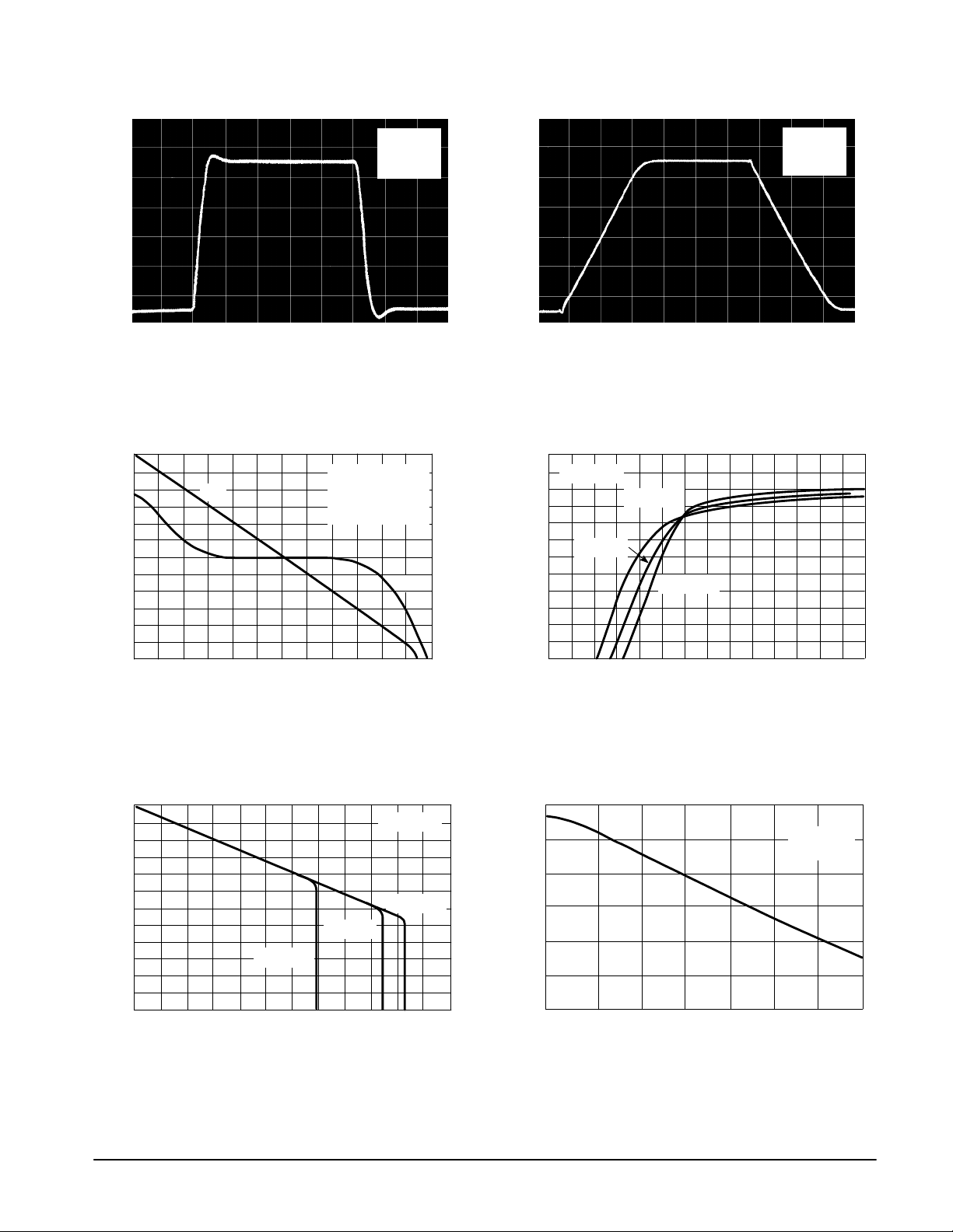
Figure 1. Timing Resistor versus
Oscillator Frequency
16
3.3 nF
)
14
Ω
12
10
8.0
, TIMING RESISTOR (k
T
R
6.0
4.0
10 k 30 k 50 k 300 k 500 k100 k 1.0 M
5.0 nF
CT=
10 nF
VCC=15V
°
C
TA=25
f
osc, OSCILLATOR FREQUENCY (Hz)
500 pF
1.0 nF
2.2 nF
100 pF
220 pF
330 pF
4
Figure 2. Maximum Output Duty Cycle
50
48
46
44
VCC=15V
42
, DUTY CYCLE MAXIMUM (%)
RT= 4.0 k to 16 k
CL=15pF
max
40
TA = 25
DC
38
10 k 30 k 50 k 300 k 500 k100 k 1.0 M
versus Oscillator Frequency
°
f
osc, OSCILLATOR FREQUENCY (Hz)
Output 2
Output 1
MOTOROLA ANALOG IC DEVICE DATA
MC34065 MC33065
Figure 3. Error Amp Small–Signal
Transient Response
2.55 V
2.50 V
2.45 V
1.0 µs/DIV
Figure 5. Error Amp Open Loop Gain and
Phase versus Frequency
100
80
60
40
20
Gain
VCC=15V
AV= –1.0
TA=25
VCC=15V
VO= 1.5 V to 2.5 V
RL= 100 k
°
C
TA=25
Phase
°
C
0
30
60
90
120
3.0 V
2.5 V
20 mV/DIV
2.0 V
Figure 4. Error Amp Large–Signal
Transient Response
1.0 µs/DIV
Figure 6. Current Sense Input Threshold
versus Error Amp Output Voltage
0.6
VCC = 15 V
0.5
0.4
0.3
0.2
TA = 25°C
TA = 125°C
TA = –55°C
VCC=15V
AV= –1.0
°
C
TA=25
200 mV/DIV
, OPEN LOOP VOL TAGE GAIN (dB)
0
VOL
A
–20
10 100 1.0 k 10 k 100 k 1.0 M 10 M
f, FREQUENCY (Hz)
Figure 7. Reference V oltage Change
versus Source Current
0
VCC = 15 V
–4.0
–8.0
–12
–16
–20
, REFERENCE VOLTAGE CHANGE (mV)
ref
V
∆
–24
0
20 40 60 80 100 120
I
, REFERENCE SOURCE CURRENT (mA)
ref
TA = 25°C
TA = 125°C
TA = –55°C
, EXCESS PHASE (DEGREES)
150
φ
180
0.1
, CURRENT SENSE INPUT THRESHOLD (V)
0
th
V
0 1.0 2.0 3.0 4.0 7.05.0 6.0
120
100
80
60
, REFERENCE SHORT CIRCUIT CURRENT (mA)
–55
SC
I
VO, ERROR AMP OUTPUT VOLTAGE (V)
Figure 8. Reference Short Circuit Current
versus T emperature
VCC=15V
≤
0.1
R
L
–25 0 25 50 75 100 125
TA, AMBIENT TEMPERATURE (°C)
Ω
MOTOROLA ANALOG IC DEVICE DATA
5
 Loading...