

MOTOROLA MC34064, MC33064 Technical data
查询MC33064DM-5供应商
The MC34064 is an undervoltage sensing circuit specifically designed for
use as a reset controller in microprocessor-based systems. It offers the
designer an economical solution for low voltage detection with a single
external resistor. The MC34064 features a trimmed-in-package bandgap
reference, and a comparator with precise thresholds and built-in hysteresis
to prevent erratic reset operation. The open collector reset output is capable
of sinking in excess of 10 mA, and operation is guaranteed down to 1.0 V
input with low standby current. These devices are packaged in 3-pin
TO-226AA, 8-pin SO–8 and Micro–8 surface mount packages.
Applications include direct monitoring of the 5.0 V MPU/logic power
supply used in appliance, automotive, consumer and industrial equipment.
• Trimmed-In-Package Temperature Compensated Reference
• Comparator Threshold of 4.6 V at 25°C
• Precise Comparator Thresholds Guaranteed Over Temperature
• Comparator Hysteresis Prevents Erratic Reset
• Reset Output Capable of Sinking in Excess of 10 mA
• Internal Clamp Diode for Discharging Delay Capacitor
• Guaranteed Reset Operation with 1.0 V Input
• Low Standby Current
• Economical TO–226AA, SO–8 and Micro–8 Surface Mount Packages
Order this document by MC34064/D
UNDERVOLTAGE
SENSING CIRCUIT
SEMICONDUCTOR
TECHNICAL DATA
P SUFFIX
PLASTIC PACKAGE
CASE 29
(TO–226AA)
D SUFFIX
PLASTIC PACKAGE
CASE 751
(SO–8)
Pin 1. Reset
2. Input
1
2
3
3. Ground
8
1
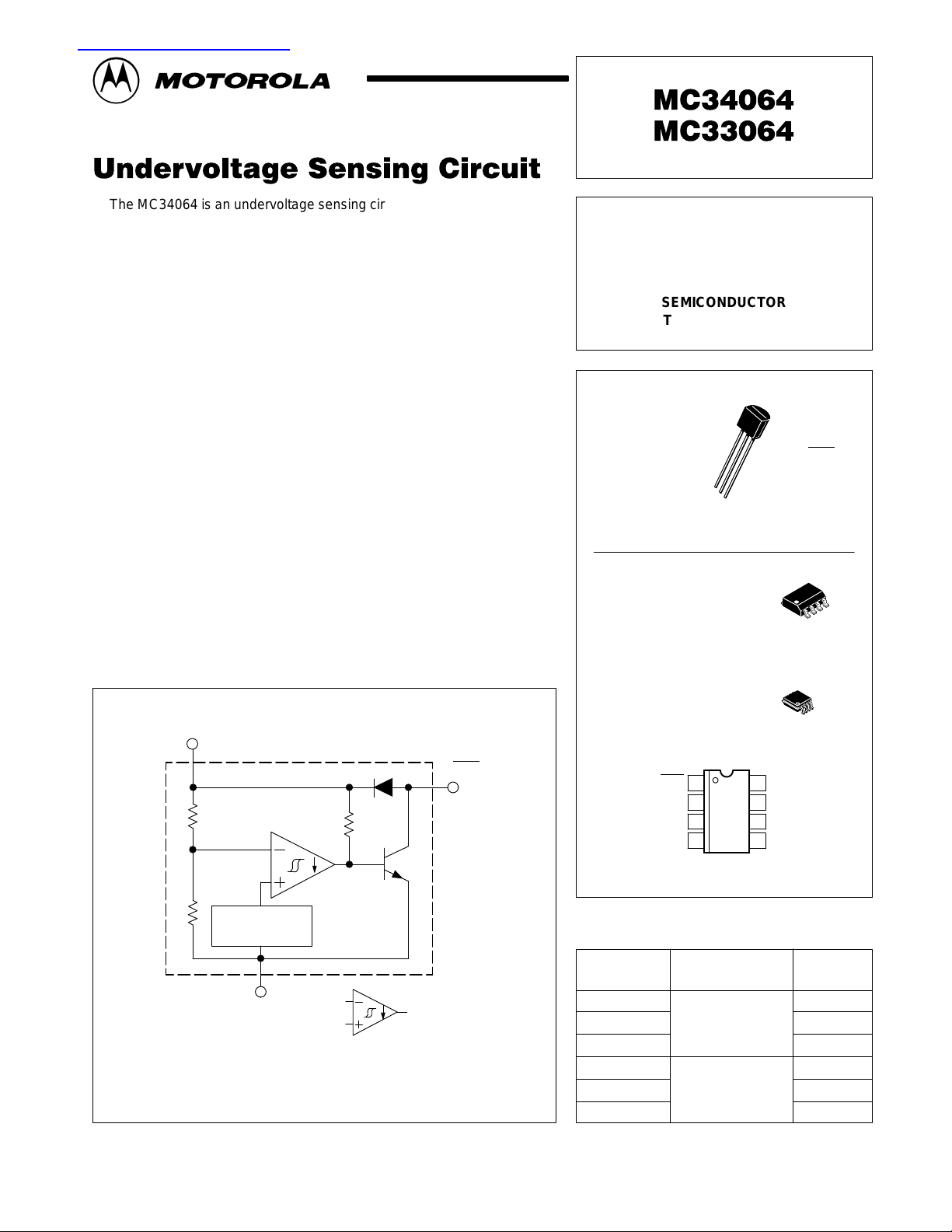
Representative Block Diagram
Input
Pin numbers adjacent to terminals are for the 3–pin TO–226AA package.
Pin numbers in parenthesis are for the 8–lead packages.
2 (2)
1.2 V
ref
3 (4)
Gnd
=
This device contains 21 active transistors.
Reset
1 (1)
Sink Only
Positive True Logic
DM SUFFIX
PLASTIC PACKAGE
CASE 846A
(Micro–8)
1
Reset
2
Input
3
N.C.
4
Ground
(Top View)
8
1
8
N.C.
7
N.C.
6
N.C.
5
N.C.
ORDERING INFORMATION
Operating
Device
MC34064D–5
MC34064DM–5 Micro–8
MC34064P–5 TO–226AA
MC33064D–5 SO–8
MC33064DM–5 Micro–8
MC33064P–5 TO–226AA
Temperature Range
TA = 0° to +70°C
TA = – 40° to +85°C
Package
SO–8
MOTOROLA ANALOG IC DEVICE DATA
Motorola, Inc. 1996 Rev 2
1
MAXIMUM RATINGS
Rating Symbol Value Unit
Power Input Supply Voltage V
Reset Output Voltage V
Reset Output Sink Current (Note 1) I
Clamp Diode Forward Current, Pin 1 to 2 (Note 1) I
Power Dissipation and Thermal Characteristics
P Suffix, Plastic Package
Maximum Power Dissipation @ TA = 25°C
Thermal Resistance, Junction–to–Air
D Suffix, Plastic Package
Maximum Power Dissipation @ TA = 25°C
Thermal Resistance, Junction–to–Air
DM Suffix, Plastic Package
Maximum Power Dissipation @ TA = 25°C
Thermal Resistance, Junction–to–Air
Operating Junction Temperature T
Operating Ambient Temperature
MC34064
MC33064
Storage Temperature Range T
NOTE: ESD data available upon request.
MC34064 MC33064
–1.0 to 10 V
10 V
Internally
Limited
100 mA
625
200
625
200
520
240
+150 °C
0 to +70
–40 to +85
–65 to +150 °C
Sink
P
R
P
R
P
R
F
θJA
θJA
θJA
T
stg
in
O
D
D
D
J
A
mA
mW
°C/W
mW
°C/W
mW
°C/W
°C
ELECTRICAL CHARACTERISTICS (For typical values T
= 25°C, for min/max values TA is the operating ambient temperature range
A
that applies [Notes 2 and 3] unless otherwise noted.)
Characteristics Symbol Min Typ Max Unit
COMPARATOR
Threshold Voltage
High State Output (Vin Increasing)
Low State Output (Vin Decreasing)
Hysteresis
V
IH
V
IL
V
H
0.01
RESET OUTPUT
Output Sink Saturation
(Vin = 4.0 V, I
(Vin = 4.0 V, I
(Vin = 1.0 V, I
Sink
Sink
Sink
= 8.0 mA)
= 2.0 mA)
= 0.1 mA)
Output Sink Current (Vin, Reset = 4.0 V) I
Output Off-State Leakage (Vin, Reset = 5.0 V) I
Clamp Diode Forward Voltage, Pin 1 to 2 (IF = 10 mA) V
V
OL
Sink
OH
F
TOTAL DEVICE
Operating Input Voltage Range V
Quiescent Input Current (Vin = 5.0 V) I
NOTES: 1. Maximum package power dissipation limits must be observed.
2.Low duty cycle pulse techniques are used during test to maintain junction temperature as close to ambient as possible.
3.T
=0°C for MC34064 T
low
–40°C for MC33064 +85°C for MC33064
= +70°C for MC34064
high
in
in
1.0 to 6.5 – – V
4.5
4.5
4.61
4.59
0.02
4.7
4.7
0.05
V
V
–
–
–
0.46
0.15
–
1.0
0.4
0.1
10 27 60 mA
– 0.02 0.5 µA
0.6 0.9 1.2 V
– 390 500 µA
2
MOTOROLA ANALOG IC DEVICE DATA
MC34064 MC33064
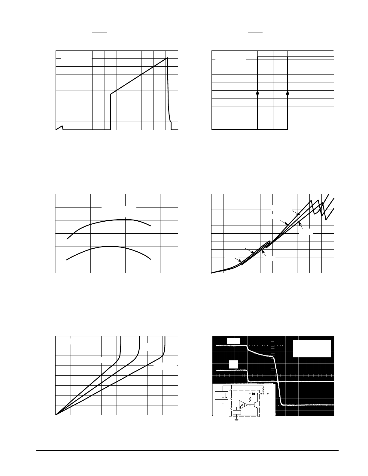
Figure 1. Reset Output Voltage versus
Input Voltage
1
RL = 10 k to V
0
TA = 25
8.0
6.0
4.0
, OUTPUT VOL TAGE (V)
O
2.0
V
0
0 2.0 4.0 6.0 8.0 1
in
°
C
Vin, INPUT VOLTAGE (V)
Figure 3. Comparator Threshold V oltage
versus T emperature
4.630
4.620
4.610
4.600
4.590
, THRESHOLD VOLTAGE (V)
th
4.580
V
RL = 10 k to V
in
Upper Threshold
High State Output
Lower Threshold
Low State Output
Figure 2. Reset Output Voltage versus
Input Voltage
5.0
RL = 10 k to V
TA = 25
4.0
3.0
2.0
, OUTPUT VOL TAGE (V)
O
1.0
V
0
0
4.56
0
in
°
C
4.58
0
Vin, INPUT VOLTAGE (V)
4.60
0
4.62
0
4.64
0
Figure 4. Input Current versus Input Voltage
1.0
0.8
0.6
0.4
, INPUT CURRENT (mA)
0.2
in
I
TA = +25
°
C
+85
°
C
TA = +25°C
–40°C
°
C
–40
+85°C
4.570
–55 –25 0 25 50 75 100 125
TA, AMBIENT TEMPERATURE (
Figure 5. Reset
Output Saturation versus
°
C)
Sink Current
2.0
V
= 4.0 V
in
1.5
1.0
, OUTPUT SA TURATION (V)
0.5
OL
V
0
010203040
TA = 85
°
C
I
, SINK CURRENT (mA)
Sink
TA = 25
°
C
TA = –40
°
C
90%
5.0 V –
4.0 V –
10%
0
0 2.0 4.0 6.0 8.0 10
Vin, INPUT VOLTAGE (V)
Delay Time
10k
Reset
200 ns/DIV
Vin = 5.0 V to 4.0 V
RL = 10 k
°
C
TA = 25
5.0V
4.0V
Figure 6. Reset
Reset
V
in
V
in
REF
MOTOROLA ANALOG IC DEVICE DATA
3
 Loading...