The MC3405 contains two differential–input operational amplifiers and
two comparators, each set capable of single supply operation. This
operational amplifier–comparator circuit fulfills its applications as a general
purpose product for automotive and consumer circuits as well as an
industrial building block.
The MC3405 is specified over the commercial operating temperature
range of 0° to +70°C.
• Operational Amplifier Equivalent in Performance to MC3403
• Comparator Similar in Performance to LM339
• Single Supply Operation: 3.0 V to 36 V
• Split Supply Operation: ±1.5 V to ±18 V
• Low Supply Current Drain
• Operational Amplifier is Internally Frequency Compensated
• Comparator TTL and CMOS Compatible
Order this document by MC3405/D
DUAL OPERATIONAL
AMPLIFIER / DUAL
VOLTAGE COMPARATOR
SEMICONDUCTOR
TECHNICAL DATA
14
1
Single Supply
3.0 V to 36 V
P SUFFIX
PLASTIC PACKAGE
CASE 646
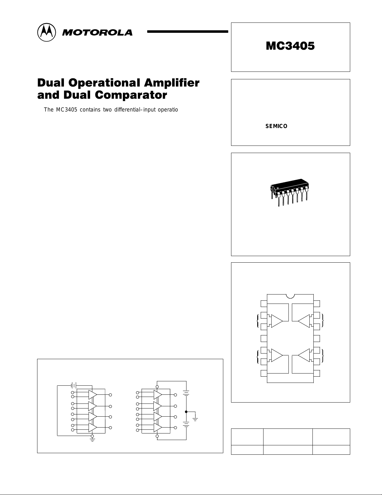
PIN CONNECTIONS
1
Out 1
Inputs 1
V
CC
Inputs 2
Split Supplies
V
CC
1
2
V
CC
1
2
1.5 V to 18 V
Out 2
Comp
1
2
(Top View)
Amp 1
Amp 2
2
+
14
–
3
4
Comp
5
+
23
–
6
7
Op
Op
14
Out 4
13
–
+
+
–
12
11
10
9
8
Inputs 4
VEE/Gnd
Inputs 3
Out 3
3
4
VEE, Gnd
MOTOROLA ANALOG IC DEVICE DATA
3
4
V
EE
1.5 V to 18 V
MC3405P TA = 0° to +70°C Plastic DIP
Motorola, Inc. 1996 Rev 1
ORDERING INFORMATION
Operating
Device
Temperature Range
Package
1

OPERATIONAL AMPLIFIER SECTION
MAXIMUM RATINGS
Rating Symbol Value Unit
Power Supply Voltage – Single Supply
Power Supply Voltage – Split Supplies
Input Differential Voltage Range V
Input Common Mode Voltage Range V
Operating Ambient Temperature Range T
Storage Temperature Range
Operating Junction Temperature Range T
VCC, V
V
IDR
ICR
Tstg
CC
EE
A
J
MC3405
0 to +70 °C
–55 to +125 °C
36
±18
±36 Vdc
±18 Vdc
150 °C
Vdc
ELECTRICAL CHARACTERISTICS (V
Characteristic
Input Offset Voltage V
Input Offset Current I
Input Bias Current I
Large–Signal, Open Loop Voltage Gain (RL = 2.0 kΩ) A
Power Supply Rejection PSR – – 150 µV/V
Output Voltage Range (Note 1) V
(RL = 10 kΩ, VCC = 5.0 V) 3.3 3.5 –
(RL = 10 kΩ, 5.0 V ≤ VCC ≤ 30 V) VCC–2.0 VCC –1.7 –
Power Supply Current (Notes 2 and 3) I
Channel Separation, f = 1.0 kHz to 20 kHz (Input Referenced) – – –120 – dB
ELECTRICAL CHARACTERISTICS (V
Characteristic
Input Offset Voltage V
(TA = T
Average Temperature Coefficient of Input Offset Voltage ∆VIO/∆T – 15 – µV/°C
Input Offset Current I
(TA = T
Input Bias Current I
(TA = T
Input Common Mode Voltage Range V
Large Signal, Open Loop Voltage Gain A
(VO = ±10 V, RL = 2.0 kΩ) 20 200 –
(TA = T
Common Mode Rejection CMR 70 90 – dB
Power Supply Rejection Ratio PSRR – 30 150 µV/V
Output Voltage V
(RL = 10 kΩ) ±12 ±13.5 –
(RL = 2.0 kΩ) ±10 ±13 –
(RL = 2.0 kΩ, TA = T
Output Short Circuit Current I
Power Supply Current (Notes 2 and 3) ICC, I
Phase Margin φm – 60 – Degrees
Small–Signal Bandwidth (AV = 1, RL = 10 kΩ, VO = 50 mV) BW – 1.0 – MHz
NOTES: 1. Output will swing to ground.
+ T
low
low
low
low
2.Not to exceed maximum package power dissipation.
3.For operational amplifier and comparator.
4.T
low
) (Note 4) – – 12
high
to T
to T
to T
= 0°C, T
) (Note 4) – – 200
high
) (Note 4) – – –800
high
) (Note 4) 15 100 –
high
high
to T
low
= +70°C
) (Note 4) ±10 – –
high
= 5.0 V, VEE = Gnd, TA = 25°C, unless otherwise noted.)
CC
Symbol Min Typ Max Unit
IO
IO
IB
VOL
OR
CC
= +15 V, VEE = –15 V, TA = 25°C, unless otherwise noted.)
CC
Symbol Min Typ Max Unit
IO
IO
IB
ICR
VOL
O
SC
EE
– 2.0 10 mV
– 30 50 nA
– –200 –500 nA
20 200 – V/mV
– 2.5 7.0 mA
– 2.0 10 mV
– – 50 nA
– –200 –500 nA
+13 –V
±10 ±20 ±45 mA
– 2.8 7.0 mA
EE
V
pp
– – Vdc
V
/mV
Vdc
2
MOTOROLA ANALOG IC DEVICE DATA

MC3405
ELECTRICAL CHARACTERISTICS (V
Characteristic
Power Bandwidth (AV = 1, RL = 2.0 kΩ, VO = 20 Vpp, THD = 5%) BWp – 9.0 – kHz
Rise Time/Fall Time t
Overshoot (AV = 1, RL = 10 kΩ, VO = 50 mV) os – 20 – %
Slew Rate SR – 0.6 – V/µs
= +15 V, VEE = –15 V, TA = 25°C, unless otherwise noted.)
CC
Symbol Min Typ Max Unit
TLH
, t
THL
– 0.35 – µs
COMPARATOR SECTION
MAXIMUM RATINGS
Rating Symbol Value Unit
Power Supply Voltage – Single Supply V
Power Supply Voltage – Split Supplies VCC, V
Input Differential Voltage Range V
Input Common Mode Voltage Range V
Sink Current I
Operating Ambient Temperature Range T
Storage Temperature Range
Operating Junction Temperature Range T
CC
IDR
ICR
Sink
A
Tstg
EE
J
36 Vdc
±18
±36 Vdc
–0.3 to +36 Vdc
20 mA
0 to +70 °C
–55 to +125 °C
150 °C
ELECTRICAL CHARACTERISTICS (V
Characteristic
Input Offset Voltage V
(TA = T
Average Temperature Coefficient of Input Offset Voltage ∆VIO/∆T – 15 – µV/°C
Input Offset Current I
(TA = T
Input Bias Current I
(TA = T
Input Common Mode Voltage Range V
(TA = T
Input Differential Voltage
(All Vin ≥ 0 Vdc)
Large–Signal, Open Loop Voltage Gain (RL = 15 kΩ) A
Output Sink Current (–Vin ≥ 1.0 Vdc, +Vin= 0, VO ≤ 1.5 V) I
Low Level Output Voltage
(+Vin= 0 V, –Vin= 1.0 V, I
(TA = T
Output Leakage Current I
(+Vin ≥ 1.0 Vdc, –Vin= 0, VO = 5.0 Vdc) – 0.1 1.0
(TA = T
Large–Signal Response – – 300 – ns
Response Time (Note 3) (VRL = 5.0 Vdc, RL = 5.1 kΩ) – – 1.3 – µs
NOTES: 1. T
to T
low
to T
low
to T
low
to T
low
to T
low
to T
low
= 0°C, T
low
2.VO ^ 1.4 V, RS = 0 Ω with VCC from 5.0 Vdc to 30 Vdc, and over the input common mode range 0 to VCC –1.7 V.
3.The response time specified is for a 100 mV input step with 5.0 mV overdrive. For larger signals 300 ns is typical.
) (Notes 1 and 2) – – 12
high
) (Note 1) – – 200
high
) (Note 1) – – –800
high
) (Note 1) 0 VCC –1.7 VCC –2.0
high
= 4.0 mA)
Sink
) (Note 1)
high
) (Note 1) – 0.1 1.0
high
= +70°C
high
= 5.0 V, VEE = Gnd, TA = 25°C, unless otherwise noted.)
CC
Symbol Min Typ Max Unit
IO
IO
IB
ICR
V
ID
VOL
Sink
V
OL
OL
6.0 16 – mA
– 2.0 10 mV
– 50 100 nA
– –125 –500 nA
0 VCC –1.5 VCC –1.7 Vpp
– – 36 V
– 200 – V
–
–
350
–
500
700
/mV
µA
µA
MOTOROLA ANALOG IC DEVICE DATA
3

MC3405
CC
V
(–)
2, 6 3, 5
(+)
Output
8,14
Q41
Q1
11
/Gnd
EE
V
700
Comparator Side
2.4 k
Comparators
to All Op Amps and
Bias Circuitry Common
Output
25
1,7
Q34
Q35
Q40
Q36
Q37
Q38
Q39
Q43
Q42
Q28
Q12
Q11
4
Q32Q31
Q33
Q29
Q26 Q30
Q27
Q16
Q15
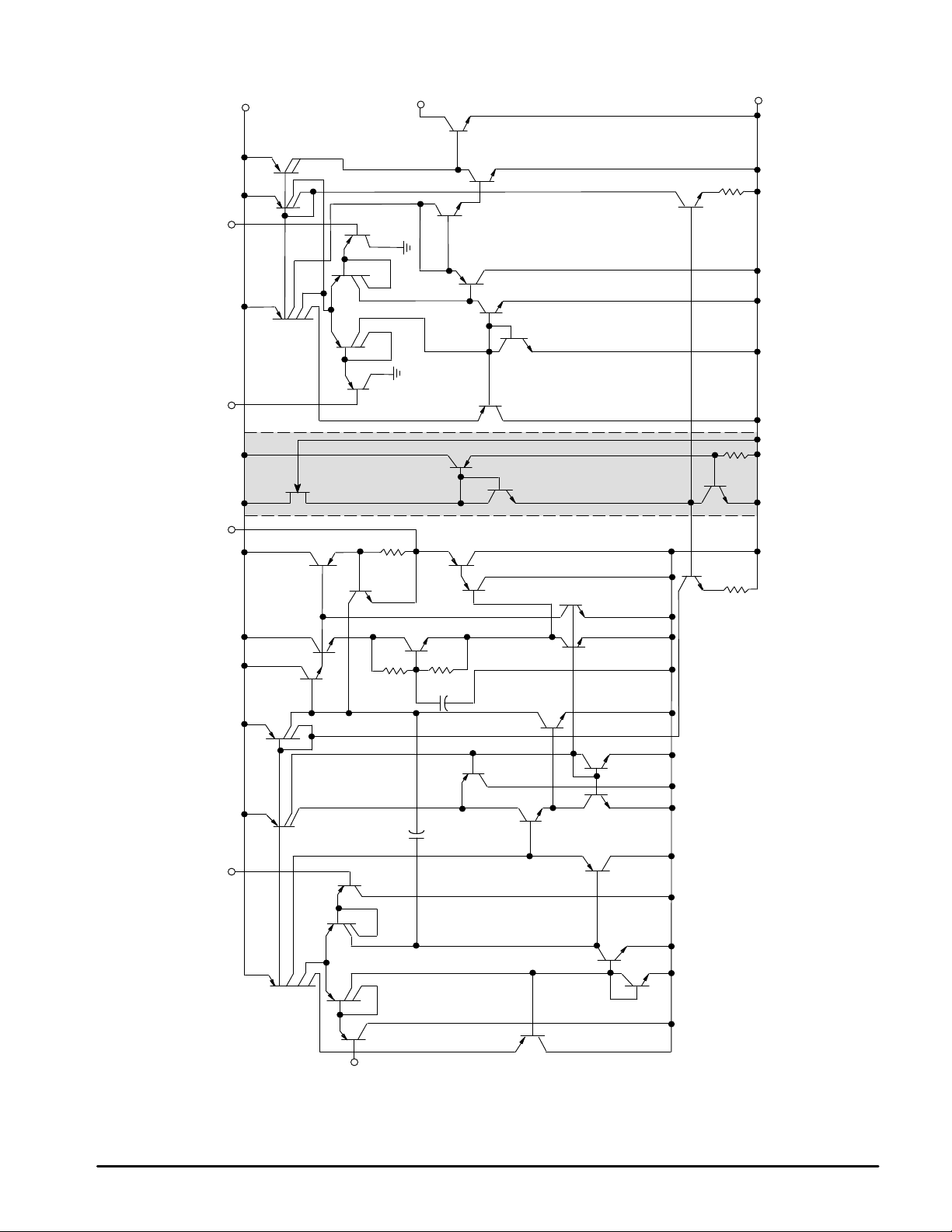
(1/2 of Circuit Shown)
Q17Q18
Representative Schematic Diagram
Q19
Q20
10,12
(+)
Q21
Q22Q24
Q23
Q25
(–)
9, 13
Q14
Q13
34.4 k
30
31.2 k
pF
Q7
Q6
5.0 pF
Q2
Q10
Q9
Q8
Q27
Q5
Q4
Q3
2.0 k
Operational Amplifier Side
4
MOTOROLA ANALOG IC DEVICE DATA
 Loading...