Motorola MC34058FTA, MC34059FTA Datasheet

SEMICONDUCTOR
TECHNICAL DATA
HEX EIA–485 TRANSCEIVER
with THREE–STATE OUTPUTS
Order this document by MC34058/D
FTA SUFFIX
PLASTIC PACKAGE
CASE 932
(Thin QFP)
148
Device
Operating
Temperature Range
Package
ORDERING INFORMATION
MC34058FTA
MC34059FTA
TA = 0° to +70°C TQFP–48
1
MOTOROLA ANALOG IC DEVICE DATA
The Motorola MC34058/9 Hex Transceiver is composed of six
driver/receiver combinations designed to comply with the EIA–485 standard.
Features include three–state outputs, thermal shutdown for each driver, and
current limiting in both directions. This device also complies with EIA–422
and CCITT Recommendations V.11 and X.27.
The devices are optimized for balanced multipoint bus transmission at
rates to 20 MBPS (MC34059). The driver outputs/receiver inputs feature a
wide common mode voltage range, allowing for their use in noisy
environments. The current limit and thermal shutdown features protect the
devices from line fault conditions.
The MC34058/9 is available in a space saving 7.0 mm 48 lead surface
mount quad package designed for optimal heat dissipation.
• Meets EIA–485 Standard for Party Line Operation
• Meets EIA–422A and CCITT Recommendations V.11 and X.27
• Operating Ambient Temperature: 0°C to +70°C
• Common Mode Driver Output/Receiver Input Range: –7.0 to +12 V
• Positive and Negative Current Limiting
• Transmission Rates to 14 MBPS (MC34058) and 20 MBPS (MC34059)
• Driver Thermal Shutdown at 150°C Junction Temperature
• Thermal Shutdown Active Low Output
• Single +5.0 V Supply, ±10%
• Low Supply Current
• Compact 7.0 mm 48 Lead TQFP Plastic Package
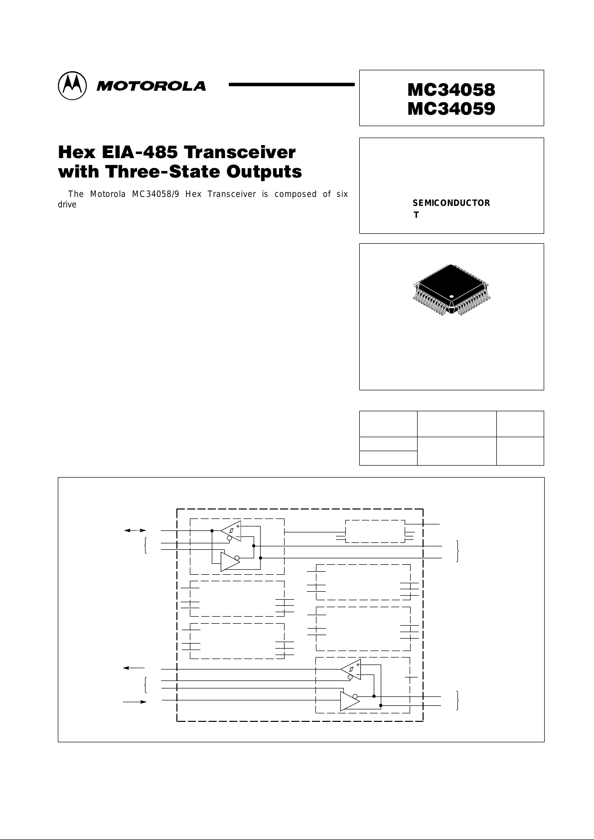
Representative Block Diagram
This device contains 1,399 active transistors.
TTL/CMOS Data DR
Direction
Control
RE
DE
Thermal
Shutdown
OB
OA
To Cable
Thermal
Shutdown
(Same as #1)
(Same as #1)
(Same as #1)
(Same as #1)
#3
#5
#4
#2
#1
TSD
#6
TSD
OB
OA
To Cable
TTL/CMOS Data RO
Direction
Control
RE
DE
TTL/CMOS Data DI
D
D
Motorola, Inc. 1996 Rev 1

MC34058 MC34059
2
MOTOROLA ANALOG IC DEVICE DATA
MAXIMUM RATINGS
Rating Symbol Value Unit
Power Supply Voltage
V
CC
–0.5, 7.0
Vdc
Input Voltage (Driver Data, Enables)
V
in
7.0
Vdc
Applied Driver Output Voltage When in Three–State
V
Z
–10, 14
Vdc
Condition (VCC = 5.0 V)
Applied Driver Output Voltage When VCC = 0 V
V
X
±14
Vdc
Output Current
I
O
Self Limiting
–
Storage Temperature
T
stg
–65, 150
°C
NOTE: Devices should not be operated at these limits. The “Recommended Operating Conditions”
provides for actual device operation.
RECOMMENDED OPERATING CONDITIONS (All limits are not necessarily functional concurrently.)
Characteristic
Symbol Min Typ Max Unit
Power Supply Voltage
V
CC
4.5
5.0
5.5
Vdc
Input Voltage (All Inputs Except Receiver Inputs)
V
in
0
–
V
CC
Vdc
Driver Output Voltage in Three–State Condition,
V
CM
–7.0
–
12
Vdc
Receiver Inputs, or When VCC = 0 V
БББББББББББББ
Driver Output Current (Normal Data Transmission)
ÁÁÁ
I
O
ÁÁÁ
–60
ÁÁÁÁ–ÁÁÁ60Á
mA
БББББББББББББ
Á
Operating Ambient Temperature
ÁÁÁ
Á
T
A
ÁÁÁ
Á
0
ÁÁÁÁ
Á
–
ÁÁÁ
Á
70
Á
Á
°C
ELECTRICAL CHARACTERISTICS (T
A
= 25°C, VCC = 5.0 V ± 10%)
Characteristic
Symbol Min Typ Max Unit
DRIVER CHARACTERISTICS
Output Voltage
ÁÁÁ
Single Ended, IO = 0 V
O
0 – V
CC
Vdc
Differential, Open Circuit (IO = 0) |V
OD1
| 1.5 – – Vdc
Differential, RL = 54 Ω |V
OD2
| 1.5 – – Vdc
Change in Differential V oltage (Note 1), RL = 54 Ω |∆V
OD2
| – – 200 mVdc
Differential, RL = 100 Ω |∆V
OD2A
| 2.0 – – Vdc
Change in Differential V oltage (Note 1), RL = 100 Ω |V
OD2A
| – – 200 mVdc
Common Mode Voltage, RL = 54 Ω V
OCM
– – 3.0 Vdc
Common Mode Voltage Change, RL = 54 Ω |∆V
OCM
| – – 200 mVdc
Output Current (Each Output)
ÁÁÁ
mA
Short Circuit Current, –7.0 V ≤ VO ≤ 12 V I
OS
–250 – 250
Driver Data Inputs
ÁÁÁ
Vdc
Low Level Voltage V
ILD
– – 0.8
High Level Voltage V
IHD
2.0 – –
Clamp Voltage (Iin = –18 mA) V
IKD
–1.5 – –
Thermal Shutdown Junction Temperature
T
JTS
–
150
–
ÁÁÁ
°C
RECEIVER CHARACTERISTICS
БББББББББББББББББ
Á
БББББББББББББББББ
Á
Input Threshold RO = High
RO = Low
Input Loading (Driver Disabled)
Hysteresis
ÁÁÁ
Á
ÁÁÁ
Á
V
th
V
H
ÁÁ
Á
ÁÁ
Á
–
–200
–
–
ÁÁ
Á
ÁÁ
Á
–
–
0.36
100
ÁÁ
Á
ÁÁ
Á
200
–
1.0
–
ÁÁÁ
ÁÁ
Á
ÁÁ
Á
mVdc
U.L.
mV
Output Voltage High (IOH = –400 µA)
Low (IOL = 4.0 mA)
V
OHR
V
OLR
2.4
–
–
–
–
0.4
ÁÁÁ
Vdc
Output Short Circuit Current
I
OSR
–
45
85
ÁÁÁ
mA
Output Leakage Current When in Three–State Mode I
OLKR
– – 20 µA
NOTE: 1. Input switched from low to high.

MC34058 MC34059
3
MOTOROLA ANALOG IC DEVICE DATA
ELECTRICAL CHARACTERISTICS (continued) (T
A
= 25°C, VCC = 5.0 V ± 10%)
Characteristic UnitMaxTypMinSymbol
MISCELLANEOUS
Enable Inputs
ÁÁÁ
Vdc
Low Level Voltage V
ILE
0 – 0.8
High Level Voltage V
IHE
2.0 – V
CC
Clamp Voltage (Iin = –18 mA) V
IKE
–1.5 – –
Power Supply Current (Total Package, All Outputs Open, Enabled
or Disabled)
I
CC
–
18
28
ÁÁÁ
mA
БББББББББББББББББ
Á
БББББББББББББББББ
Á
Thermal Shutdown Output Voltage
High
Low
ÁÁÁ
Á
ÁÁÁ
Á
V
OHT
V
OLT
ÁÁ
Á
ÁÁ
Á
2.4
0
ÁÁ
Á
ÁÁ
Á
–
–
ÁÁ
Á
ÁÁ
Á
–
0.8
ÁÁÁ
ÁÁ
Á
ÁÁ
Á
Vdc
TIMING CHARACTERISTICS – DRIVER
Propagation Delay – Input to Single Ended Output
ns
Input to Output – Low–to–High t
PLH
– 10 20
Input to Output – High–to–Low t
PHD
– 11 20
Propagation Delay – Input to Differential Output
ÁÁÁ
ns
Input Low–to–High t
PLHD
– 15 23
Input High–to–Low t
PHLD
– 15 23
Differential Output Transition T ime
tDR, t
DF
–
9.0
10.7
ÁÁÁ
ns
Skew Timing MC34058 ns
|t
PLHD
– t
PHLD
| for Each Driver t
SK1
0 0.1 –
Maximum – Minimum t
PLHD
Within a Package t
SK2
0 – 8.0
Maximum – Minimum t
PHLD
Within a Package t
SK3
0 – 6.0
Skew Timing MC34059 ns
|t
PLHD
– t
PHLD
| for Each Driver t
SK7
0 0.1 –
Propagation Delay Difference Between Any Two Drivers (Same
Package or Different Packages at Same VCC and TA)
t
SK8
– <4.0 –
Enable Timing ns
Single Ended Outputs
Enable to Active High Output t
PZH
– 15 40
Enable to Active Low Output t
PZL
– 25 40
Active High to Disable t
PHZ
– 12 25
Active Low to Disable t
PLZ
– 10 25
Differential Outputs
Enable to Active Output t
PZD
– – 40
Enable to Three–State Output t
PDZ
– – 25
TIMING CHARACTERISTICS – RECEIVER
Propagation Delay ns
Input to Output – Low–to–High t
PLHR
– 16 23
Input to Output – High–to–Low t
PHLR
– 16 23
Skew Timing ns
|t
PLHR
– t
PHLR
| for Each Receiver t
SK4
0 1.0 –
Maximum – Minimum t
PLHR
Within a Package t
SK5
0 – 3.0
Maximum – Minimum t
PHLR
Within a Package t
SK6
0 – 3.0
Skew Timing t
SK9
– <5.0 – ns
Propagation Delay Difference Between Any Two Receivers in Different
Packages at Same VCC and TA (MC34059 Only)
Enable Timing ns
Single Ended Outputs
Enable to Active High Output t
PZHR
– 15 22
Enable to Active Low Output t
PZLR
– 25 30
Active High to Disable t
PHZR
– 12 25
Active Low to Disable t
PLZR
– 10 25

MC34058 MC34059
4
MOTOROLA ANALOG IC DEVICE DATA
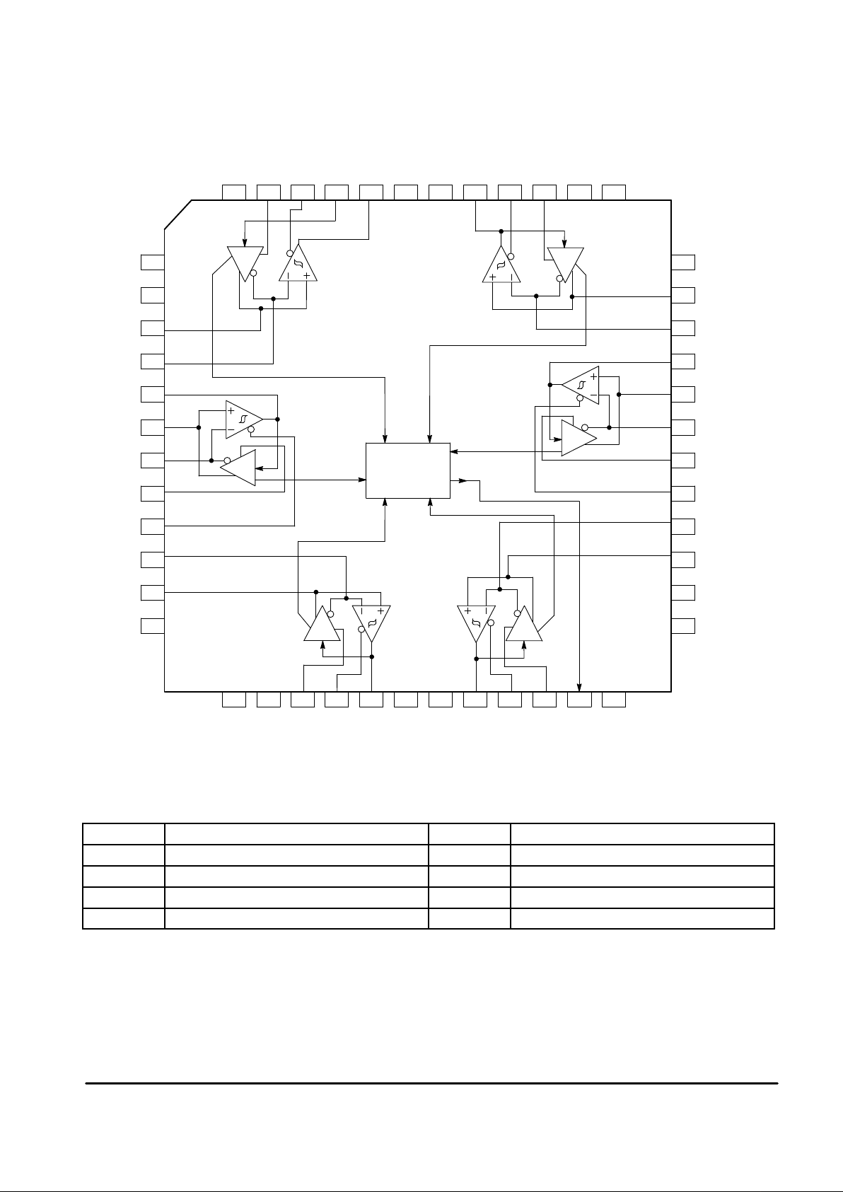
Block Diagram and Pinout
MC34058/9
Thermal
Shutdown
Indicator
Gnd
1
Gnd Gnd Gnd
GndDE5RE5DR5V
CC
V
CC
RO6DI6RE6DE6
DE2 RE2 DR2 VCCVCCDR3 RE3 DE3 TSD
Gnd
OA5
OB5
DR4
OA4
OB4
DE4
RE4
OB3
OA3
Gnd
Gnd
#4
#5
#6
#3
#2
#1
Gnd
Gnd
OA6
OB6
DR1
OA1
OB1
DE1
RE1
OB2
OA2
Gnd
2
3
4
5
6
7
8
9
10
11
12
36
35
34
33
32
31
30
29
28
27
26
18 19 20 21 22 23 24
25
1716151413
43 42 41 40 39 38 374445464748
Gnd
D
D
D
D
D
D
PINOUT SUMMARY
OA NonInverting Output/Input DE Driver Enable, Active High (TTL)
OB Inverting Output/Input RE Receiver Enable, Active Low (TTL)
DR Driver Input/Receiver Output (TTL) TSD Thermal Shutdown Indicator
DI6 #6 Driver Input (TTL) V
CC
Connect 4 Pins to 5.0 V , ±10%
RO6 #6 Receiver Output (TTL) Gnd Connect 12 Pins to Circuit Ground
 Loading...