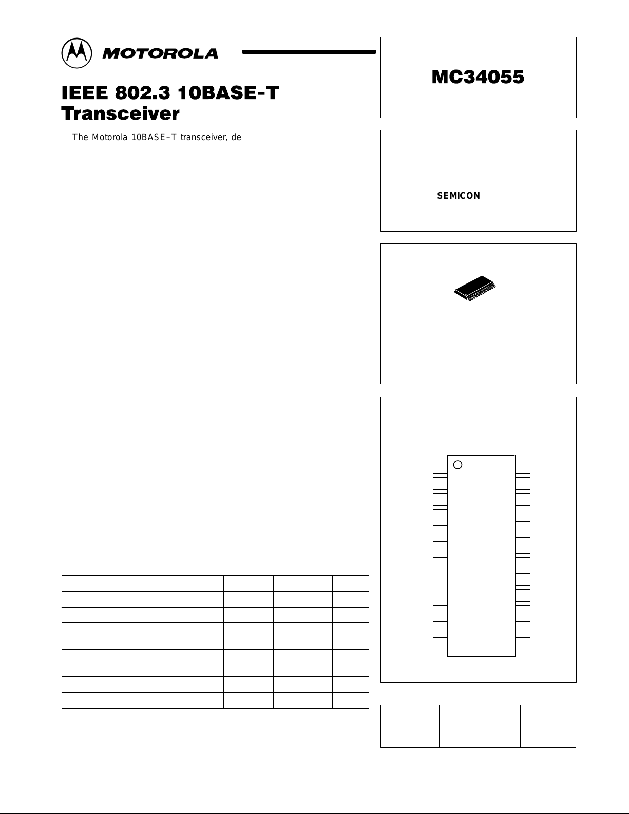
The Motorola 10BASE–T transceiver, designed to comply with the ISO
8802–3 [IEEE 802.3] 10BASE–T specification, will support a Medium
Dependent Interface (MDI) in an embedded Media Attachment Unit (MAU)*.
The interface supporting the Data T erminal Equipment (DTE) is TTL, CMOS,
and raised ECL compatible, and the interface to the Twisted Pair (TP) media
is supported through standard 10BASE–T filters and transformers.
Differential data intended for the TP media is provided a 50 ns pre–emphasis
and data at the TP receiver is screened by Smart Squelch circuitry for
specific threshold, pulse width, and sequence requirements.
Other features of the MC34055 include: Collision and Jabber detection
status outputs, select mode pins for forcing Loop Back and Full–Duplex
operation, a Signal Quality Error pin for testing the collision detect circuitry
without affecting the TP output, and a LED driver for Link Integrity status. An
on–chip oscillator, capable of receiving a clock input or operating under
crystal control, is also provided for internal timing and driving a buffered
clock output.
The MC34055 is manufactured on a BiCMOS process and is packaged in
a 24 pin SOIC.
• BiCMOS Technology for Low Power Operation
• Standard 5.0 V, ± 5% Voltage Supply
• Smart Squelch Enforcement of Threshold, Pulse Width, and Sequence
Requirements
• Driver Pre–Emphasis for Output Data
• TTL, CMOS and Raised ECL Compatible
• Interfaces to TP Media with Standard 10BASE–T Filters and
Transformers
• LED Capable Status Outputs for Collision, Jabber Detection, and Link
Integrity
• Directly Driven or Crystal Controlled Clock Oscillator
• Selectable Full–Duplex Operation
• Signal Quality Error Test Pin
• Selectable Loop Back
MAXIMUM RATINGS
Power Supply Voltage V
Differential V oltage at RX+/RX– V
Voltage Applied to Logic and Mode/Test
Select Inputs
Voltage Applied to Logic Outputs and
Output Status Pins
Ambient Operating Temperature Range T
Junction Temperature T
NOTE: Devices should not be operated at these limits. The “Recommended Operating
Conditions” table provides for actual device operation.
(TA = 25°C, unless otherwise noted.)
Rating Symbol Value Unit
CC
ID
A
J
– 0.5 to 7.0 Vdc
– 5.25 to 5.25 Vdc
– 0.5 to 5.5 Vdc
– 0.5 to 7.0 Vdc
0 to 70 °C
– 65 to 150 °C
Order this document by MC34055/D
10BASE–T TRANSCEIVER
SEMICONDUCTOR
TECHNICAL DATA
24
1
DW SUFFIX
PLASTIC PACKAGE
CASE 751E
(SO–24L)
PIN CONNECTIONS
Clk Out
TX Data A
TX Data B
TX EN H
Dig. Gnd
VCC(Dig/Ana)
Ana. Gnd
RX Data A
RX Data B
RX EN H
LNKFL H JABB H
Loop L
1
2
3
4
5
6
7
8
9
10
11
12
ORDERING INFORMATION
Operating
Device
MC34055DW TA = 0° to +70°C SO–24L
Temperature Range
24
23
22
21
20
19
18
17
16
15
14
13
Clk+
Clk–
SQE EN L
TX+
TX–
Pwr Gnd
Pwr V
CC
FULLD L
RX+
RX–
CTL H
Package
MOTOROLA ANALOG IC DEVICE DATA
Motorola, Inc. 1996 Rev 1
1
Balun
V
CC
TX+
Filter
TX–
Loop L
RX+
Filter
RX–
FULLD L
LNKFL H
TP Differential
Driver and Control
Loop Back
TP Differential Receiver
with Smart Squelch
Full Duplex Disable
Duplex Mode
Select
Link Fail Disable
TTL/CMOS
MC34055
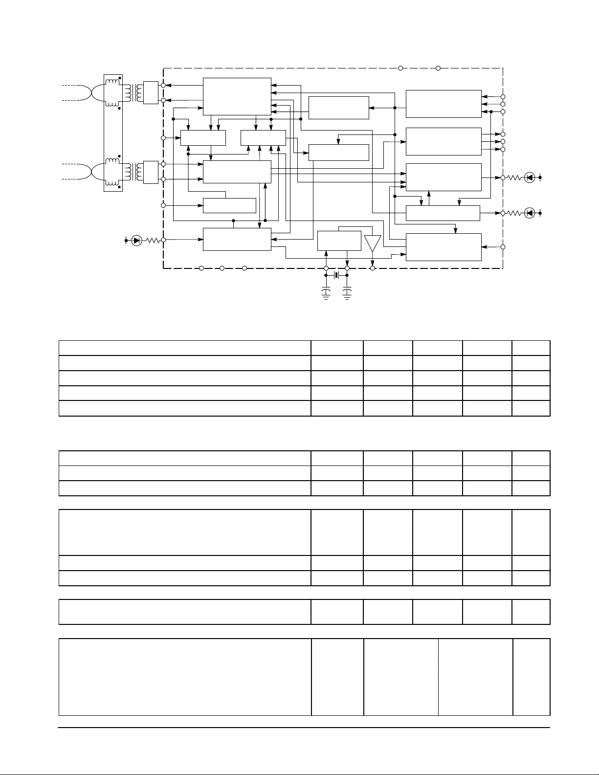
Simplified Block Diagram
Driver Pre–Emphasis
Collision
Detect
Link Beat
Control
Jabber Disable
Transmit Idle
Collision Announcement
Link Pulse
Clock Oscillator
TTL/CMOS
Timer
Data In
Collision T est
Data Out
VCC (Dig/Ana)Pwr V
CC
Transmit Input
and Control
Received Data
Output and
Control
Collision
Detect
Outputs
Jabber
Signal
Quality
Error
CMOS
ECL
TTL/CMOS
TTL/CMOS
ECL
TTL/CMOS
TTL/CMOS
TTL/CMOS
TTL/CMOS
TX Data A
TX Data B
TX EN H
RX Data A
RX Data B
RX EN H
CTL H
JABB H
SQE EN L
V
CC
V
CC
Clk–Clk +
Clk
Out
*The sale and use of this product is licensed
*under technology covered by one or more
*Digital Equipment Corporation patents.
Ana.
Gnd
Dig.
Pwr
Gnd
Gnd
10MHz
This device contains 9,875 active transistors.
RECOMMENDED OPERATING CONDITIONS
Characteristic Symbol Min Typ Max Unit
Power Supply Voltage V
CC
Voltage Applied to Logic Inputs and Status Pins – 0 – 5.25 Vdc
Differential Input Voltage – 0.59 – 2.8 Vpp
Operating Ambient Temperature T
NOTE: All limits are not necessarily functional concurrently.
ELECTRICAL CHARACTERISTICS (0°C ≤ T
≤ 70°C, VCC = 5.0 V, unless otherwise noted.)
A
A
Characteristic Symbol Min Typ Max Unit
Supply Current (4.75 V ≤ VCC ≤ 5.25 V) I
CC
Reset Circuit Threshold – 4.0 – 4.4 Vdc
TWISTED PAIR TRANSMITTER
Output Differential V oltage
(See Load Circuits: Differential Load Circuit)
V
O
Output Differential Voltage with Pre–Emphasis 2.2 2.53 2.8
Output Differential V oltage 1.56 1.72 1.98
Common Mode Driver Impedance Z
Transmitter Differential Output Impedance Z
OCM
OD
TX DATA A
Input High Voltage (IIH = + 20 µA) V
Input Low Voltage (IIL = –150 µA) V
IH
IL
TX DATA B
Input Voltage (See Load Circuits: ECL Load Circuit)
High: @ 0°C V
IH
@ 25°C 0.984 VCC– 0.877 0.984 VCC– 0.727
@ 70°C 0.984 VCC– 0.825 0.984 VCC– 0.644
Low: @ 0°C V
IL
@ 25°C 0.750 VCC– 0.550 0.750 VCC– 0.350
@ 70°C 0.750 VCC– 0.531 0.750 VCC– 0.324
4.75 5.0 5.25 Vdc
0 – 70 °C
– 60 180 mA
6.0 8.5 14 Ω
8.0 15.5 29 Ω
3.15 – 5.25 Vdc
0 – 0.8
0.984 VCC– 0.923 0.984 VCC– 0.763
0.750 VCC– 0.568 0.750 VCC– 0.361
Vpp
Vdc
2
MOTOROLA ANALOG IC DEVICE DATA
MC34055
ELECTRICAL CHARACTERISTICS (0°C ≤ T
Characteristic Symbol Min Typ Max Unit
TX EN H
Input High Voltage (IIH = 200 µA) V
Input Low Voltage (IIL = – 20 µA) V
RX DATA A/RX EN H/JABB H/CTL H
Output Voltage (See Load Circuits: CMOS Load Circuit)
High (IOH = –12 mA) V
Low (IOL = +16 mA) V
RX DATA B
Output Voltage (See Load Circuits: ECL Load Circuit)
High: @ 0°C V
@ 25°C 0.984 VCC– 0.877 0.984 VCC– 0.727
@ 70°C 0.984 VCC– 0.825 0.984 VCC– 0.644
Low: @ 0°C V
@ 25°C 0.750 VCC– 0.550 0.750 VCC– 0.350
@ 70°C 0.750 VCC– 0.531 0.750 VCC– 0.324
SIGNAL QUALITY ERROR TEST ENABLE CONTROL (SQE EN L)
Test Control Voltage
Test Disabled (Input High Voltage)(IIH = + 20 µA Max.) V
Test Enabled (Input Low Voltage)(– 50 µA < IIL < –150 µA) V
FULL DUPLEX MODE SELECT (FULLD L)
Mode Select Control Voltage
Normal Operation (Input High)(IIH = + 20 µA) V
Full Duplex (Input Low)(– 50 µA < IIH < –150 µA) V
LOOPBACK TEST MODE FUNCTION (LOOP L)
Test Control Voltage
Test Disabled (Input High)(IIH = + 20 µA) V
Test Enabled (Input Low)(IIL = – 200 µA) V
LINK FAIL STATUS (LINKFL H)
Status Output Voltage (See Load Circuits: CMOS Load Circuit)
Maximum Voltage for Output Low Condition (IOL = 20 mA) V
Output Low Sink Current V
CLOCK OSCILLATOR
Clk+ Input Logic Threshold
High Level Input Voltage (IIH = +100 µA Max.) V
Logic Low Input Voltage (IIL = –100 µA Max.) V
Clk Out Output Voltage (See Load Circuits: CMOS Load Circuit)
Logic High (IOH = –12 mA) V
Logic Low (I
= +16 µA) V
out
≤ 70°C, VCC = 5.0 V, unless otherwise noted.)
A
IH
IL
OH
OL
OH
OL
IH
IL
IH
IL
IH
IL
OH
OL
IH
IL
OH
OL
2.0 – 5.0 Vdc
0 – 0.8
Vdc
3.7 – –
– – 0.5
Vdc
0.984 VCC– 0.923 0.984 VCC– 0.763
0.750 VCC– 0.568 0.750 VCC– 0.361
Vdc
2.0 – 5.0
0 – 0.8
Vdc
2.0 – 5.0
0 – 0.8
Vdc
2.0 – 5.0
0 – 0.8
– – 0.5 Vdc
– – 20 mA
2.0 – 5.0 Vdc
– – 0.8 µA
Vdc
3.7 3.9 –
– 0.25 0.5
Ω
15 pF
ECL Load Circuit
330
MOTOROLA ANALOG IC DEVICE DATA
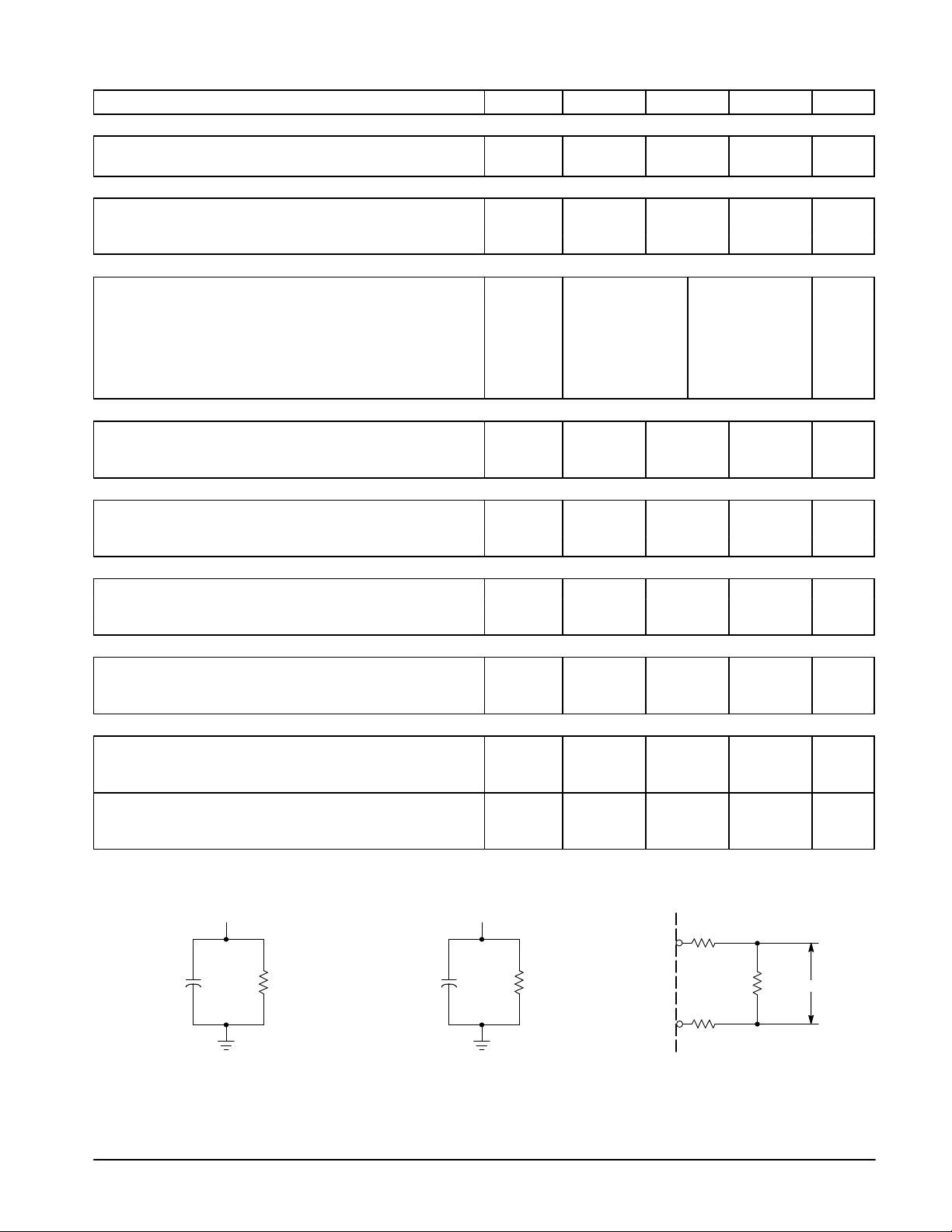
Output Load Circuits
20 pF
TTL/CMOS Load Circuit
6.0k
39 (1%)
TX–
Ω
39 (1%)
TX+
Differential Load Circuit
100
Ω
V
OD
3
MC34055
TIMING CHARACTERISTICS
TRANSMIT START TIMING
TX EN H to TX+/TX– Enable Time t
TX Data A/B to TX+/TX– Enable Time t
Steady State Propagation Delay of TX Data A/B to TX+/TX– Output t
Pre–Emphasis Pulse Width t
Transmitter Caused Edge Skew Between TX+ and TX– t
Transmitter Added Edge Jitter to TX+/TX– from TX Data A/B t
Steady–State Delay between the TX Data A/B Input to the RX Data
A/B Outputs for Normal Operation
TX EN H Assert to RX EN H Assert Under Normal Operation t
TRANSMIT STOP TIMING
Delay between TX EN H Low and TX+/TX– High t
TX EN H Assert/De–assert Delay from TX EN H to RX EN H
Assert/De–assert
End of Packet Hold Time from Last TX Data A/B Edge or
TX EN H De–assert
LINK BEAT PULSES
Output Link Test Pulse Width t
Minimum Link Beat Pulse Duration on RX+/RX– t
LOOP BACK MODE TIMING
Delay from Loop L Deassertion to RX EN H Driven from
TX EN H Status
TX EN H Assert/De–assert to RX EN H, Assert/De–assert when in
Loop–Back Mode and Receiver Inactive
Steady–State TX Data A/B to RX Data A/B when in Loop–Back Mode t
SMART SQUELCH
Interval Unit Squelch Deactivation t
RECEIVE START TIMING
Receiver–Added Edge Skew to RX Data A/B Signal t
Receiver–Added Edge Jitter to RX Data A/B Signal t
Start–Up Delay from RX+/RX– to RX Data A/B t
Delay from RX EN H Assertion Until RX Data A/B Valid t
Steady–State Propagation Delay from RX+/RX– Data A/B t
RECEIVE SHUTDOWN TIMING
Last received Data Edge until the RX EN H Output forces low t
(0°C ≤ TA ≤ 70°C)
Characteristic
Symbol Min Typ Max Unit
TXEN
FDXD
TXSS
PRCM
Skew T
Jitter T
t
TXRX
DREL
TXDH
t
XTRE
t
TDDC
LKPW
LDCY_A
t
LTRA
t
LTRX
LTRD
SQ
Skew R
Jitter R
RXNE
RARE
RXSS
RXDE
– – 75 ns
– – 75 ns
– – 75 ns
45 – 55 ns
– – 2.0 ns
– – 4.0 ns
– – 50 ns
– – 50 ns
– – 75 ns
– – 400 ns
250 – – ns
80 – 120 ns
80 – 192 ns
– – 30 ns
– – 50 ns
– – 50 ns
– – 5.0 Bit
Times
– – 1.5 ns
– – 1.5 ns
– – 50 ns
–10 – +10 ns
– – 50 ns
155 – 250 ns
4
MOTOROLA ANALOG IC DEVICE DATA
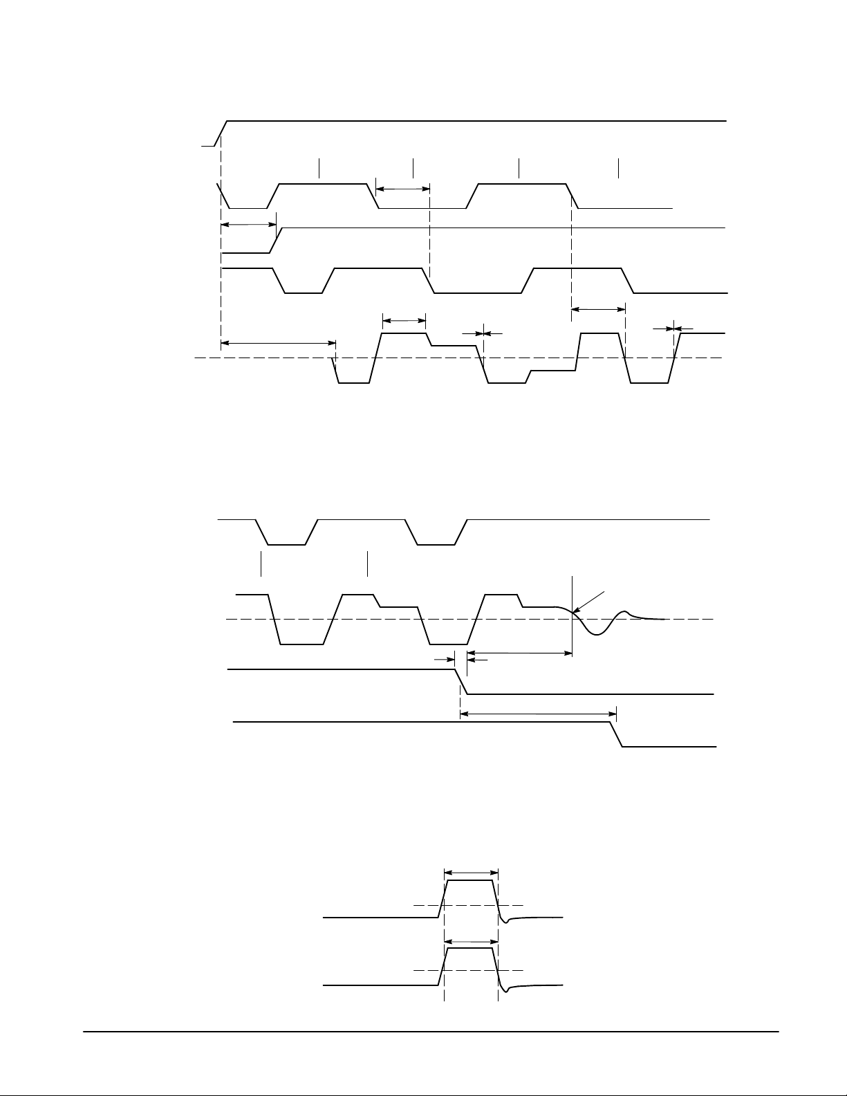
TX EN H
MC34055
Figure 1. Start Up and Steady State Transmit Timing
Bit Pattern
TX Data A/B
RX EN H
RX Data A/B
TX+/TX–
TX Data A/B
Bit Pattern
t
DREL
t
TXEN
t
TXRX
t
PRCM
t
SKEW T
Figure 2. Driver Shutdown Timing
01
0101
t
TXSS
t
JITTER T
TX+/TX–
TX EN H
RX EN H
RX+/RX–
TX+/TX–
t
TXDH
Figure 3. Link Pulse Timing
t
LDCY_A
t
LKPW
t
TDDC
t
585mV
XTRE
585mV
585mV
MOTOROLA ANALOG IC DEVICE DATA
5
 Loading...