

查询MC33025供应商
The MC34025 series are high speed, fixed frequency, double–ended
pulse width modulator controllers optimized for high frequency operation.
They are specifically designed for Off–Line and DC–to–DC converter
applications offering the designer a cost effective solution with minimal
external components. These integrated circuits feature an oscillator, a
temperature compensated reference, a wide bandwidth error amplifier, a
high speed current sensing comparator, steering flip–flop, and dual high
current totem pole outputs ideally suited for driving power MOSFETs.
Also included are protective features consisting of input and reference
undervoltage lockouts each with hysteresis, cycle–by–cycle current limiting,
and a latch for single pulse metering.
The flexibility of this series allows it to be easily configured for either
current mode or voltage mode control.
• 50 ns Propagation Delay to Outputs
• Dual High Current Totem Pole Outputs
• Wide Bandwidth Error Amplifier
• Fully–Latched Logic with Double Pulse Suppression
• Latching PWM for Cycle–By–Cycle Current Limiting
• Soft–Start Control with Latched Overcurrent Reset
• Input Undervoltage Lockout with Hysteresis
• Low Start–Up Current (500 µA Typ)
• Internally Trimmed Reference with Undervoltage Lockout
• 90% Maximum Duty Cycle (Externally Adjustable)
• Precision Trimmed Oscillator
• Voltage or Current Mode Operation to 1.0 MHz
• Functionally Similar to the UC3825
Simplified Application
V
ref
Clock
R
T
C
T
Ramp
Error Amp
Output
Noninverting
Input
Inverting
Input
Soft–Start
16
4
5
Oscillator
6
7
3
2
1
8
Error
Amp
Soft–Star
t
This device contains 227 active transistors.
5.1V
Reference
UVLO
Latching
PWM and
Steering
Flip Flop
Ground
10
15
V
CC
13
V
C
14
Output B
11
Output A
Power
Ground
12
9
Current
Limit/
Shutdown
Order this document by MC34025/D
16
1
P SUFFIX
PLASTIC PACKAGE
CASE 648
16
1
DW SUFFIX
PLASTIC PACKAGE
CASE 751G
(SO–16L)
PIN CONNECTIONS
Error Amp
Inverting Input
Error Amp
Noninverting Input
Error Amp Output
Soft–Start
ORDERING INFORMATION
Device
MC33025DW
MC33025P Plastic DIP
MC34025DW SO–16L
MC34025P
1
2
3
4
Clock
5
R
T
6
C
T
7
Ramp
8
(Top View)
Operating
Temperature Range
TA = –40° to +105°C
TA = 0° to +70°C
16
V
ref
15
V
CC
14
Output B
13
V
C
12
Power Ground
11
Output A
10
Ground
Current Limit/
9
Shutdown
Plastic DIP
Package
SO–16L
MOTOROLA ANALOG IC DEVICE DATA
Motorola, Inc. 1996 Rev 1
1
MC34025 MC33025
MAXIMUM RATINGS
Rating Symbol Value Unit
Power Supply Voltage V
Output Driver Supply Voltage V
Output Current, Source or Sink (Note 1)
DC
Pulsed (0.5 µs)
Current Sense, Soft–Start, Ramp, and Error Amp Inputs V
Error Amp Output and Soft–Start Sink Current I
Clock and RT Output Current I
Power Dissipation and Thermal Characteristics
SO–16 Package (Case 751G)
Maximum Power Dissipation @ TA = +25°C
Thermal Resistance, Junction–to–Air
DIP Package (Case 648)
Maximum Power Dissipation @ TA = +25°C
Thermal Resistance, Junction–to–Air
Operating Junction Temperature T
Operating Ambient Temperature (Note 2)
MC34025
MC33025
Storage Temperature Range T
R
R
CC
C
I
O
in
O
CO
P
D
θJA
P
D
θJA
J
T
A
stg
30 V
20 V
0.5
2.0
–0.3 to +7.0 V
10 mA
5.0 mA
862
145
1.25
100
mW
°C/W
W
°C/W
+150 °C
°C
0 to +70
–40 to +105
–55 to +150 °C
A
ELECTRICAL CHARACTERISTICS (V
= 15 V, RT = 3.65 kΩ, CT = 1.0 nF, for typical values TA = +25°C, for min/max values TA is
CC
the operating ambient temperature range that applies [Note 2], unless otherwise noted.)
Characteristic
Symbol Min Typ Max Unit
REFERENCE SECTION
Reference Output Voltage (IO = 1.0 mA, TJ = +25°C) V
Line Regulation (VCC = 10 V to 30 V) Reg
Load Regulation (IO = 1.0 mA to 10 mA) Reg
T emperature Stability T
Total Output Variation over Line, Load, and Temperature V
Output Noise Voltage (f = 10 Hz to 10 kHz, TJ = +25°C) V
ref
line
load
S
ref
n
5.05 5.1 5.15 V
– 2.0 15 mV
– 2.0 15 mV
– 0.2 – mV/°C
4.95 – 5.25 V
– 50 – µV
Long Term Stability (TA = +125°C for 1000 Hours) S – 5.0 – mV
Output Short Circuit Current I
SC
–30 –65 –100 mA
OSCILLATOR SECTION
Frequency
TJ = +25°C
Line (VCC = 10 V to 30 V) and Temperature (TA = T
low
to T
high
)
Frequency Change with Voltage (VCC = 10 V to 30 V) ∆f
Frequency Change with Temperature (TA = T
low
to T
) ∆f
high
Sawtooth Peak Voltage V
Sawtooth Valley Voltage V
f
osc
/∆V – 0.2 1.0 %
osc
/∆T – 2.0 – %
osc
P
V
380
370
400
400
420
430
2.6 2.8 3.0 V
0.7 1.0 1.25 V
Clock Output Voltage
High State
Low State
NOTES: 1. Maximum package power dissipation limits must be observed.
2.Low duty cycle pulse techniques are used during test to maintain junction temperature as close to ambient as possible.
T
= 0°C for MC34025 T
low
T
= – 40°C for MC33025 T
low
= +70°C for MC34025
high
= +105°C for MC33025
high
V
OH
V
OL
3.9
–
2.3
4.5
–
2.9
kHz
V
2
MOTOROLA ANALOG IC DEVICE DATA
MC34025 MC33025
p
th
ELECTRICAL CHARACTERISTICS (V
= 15 V, RT = 3.65 kΩ, CT = 1.0 nF, for typical values TA = +25°C, for min/max values
CC
TA is the operating ambient temperature range that applies [Note 2], unless otherwise noted.)
Characteristic
Symbol Min Typ Max Unit
ERROR AMPLIFIER SECTION
Input Offset Voltage V
Input Bias Current I
Input Offset Current I
Open–Loop Voltage Gain (VO = 1.0 V to 4.0 V) A
IO
IB
IO
VOL
– – 15 mV
– 0.6 3.0 µA
– 0.1 1.0 µA
60 95 – dB
Gain Bandwidth Product (TJ = +25°C) GBW 4.0 8.3 – MHz
Common Mode Rejection Ratio (VCM = 1.5 V to 5.5 V) CMRR 75 95 – dB
Power Supply Rejection Ratio (VCC = 10 V to 30 V) PSRR 85 110 – dB
Output Current, Source (VO = 4.0 V)
Output Current, Sink (VO = 1.0 V)
Output Voltage Swing, High State (IO = – 0.5 mA)
Output Voltage Swing, Low State (IO = 1.0 mA)
I
Source
I
Sink
V
OH
V
OL
0.5
1.0
4.5
3.0
3.6
4.75
0
0.4
–
–
5.0
1.0
Slew Rate SR 6.0 12 – V/µs
PWM COMPARATOR SECTION
Ramp Input Bias Current I
Duty Cycle, Maximum
Duty Cycle, Minimum
DC
DC
Zero Duty Cycle Threshold Voltage Pin 3(4) (Pin 7(9) = 0 V) V
Propagation Delay (Ramp Input to Output, TJ = +25°C) t
PLH(in/out)
IB
(max)
(min)
th
– –0.5 –5.0 µA
80
–
90
–
0
–
1.1 1.25 1.4 V
– 60 100 ns
SIFT–START SECTION
Charge Current (V
Soft–Start
Discharge Current (V
= 0.5 V) I
Soft–Start
= 1.5 V) I
chg
dischg
3.0 9.0 20 µA
1.0 4.0 – mA
CURRENT SENSE SECTION
Input Bias Current (Pin 9(12) = 0 V to 4.0 V) I
Current Limit Comparator Threshold
Shutdown Comparator Threshold
Propagation Delay (Current Limit/Shutdown to Output, TJ = +25°C) t
PLH(in/out)
IB
V
th
V
th
– – 15 µA
0.9
1.0
1.10
1.25 1.40 1.55
– 50 80 ns
OUTPUT SECTION
Output Voltage
Low State (I
High State (I
Output Voltage with UVLO Activated (VCC = 6.0 V, I
Output Leakage Current (VC = 20 V) I
Output Voltage Rise T ime (CL = 1.0 nF, TJ = +25°C) t
Output Voltage Fall T ime (CL = 1.0 nF, TJ = +25°C) t
Sink
(I
Sink
Source
(I
Source
= 20 mA)
= 200 mA)
= 20 mA)
= 200 mA)
= 0.5 mA) V
Sink
V
OL
V
OH
OL(UVLO)
L
r
f
–
–
13
12
0.25
1.2
13.5
13
0.4
2.2
–
–
– 0.25 1.0 V
– 100 500 µA
– 30 60 ns
– 30 60 ns
UNDERVOLTAGE LOCKOUT SECTION
Start–Up Threshold (VCC Increasing) V
UVLO Hysteresis Voltage (VCC Decreasing After Turn–On) V
th(on)
H
8.8 9.2 9.6 V
0.4 0.8 1.2 V
TOTAL DEVICE
Power Supply Current
Start–Up (VCC = 8.0 V)
Operating
NOTES: 1. Maximum package power dissipation limits must be observed.
2.Low duty cycle pulse techniques are used during test to maintain junction temperature as close to ambient as possible.
T
= 0°C for MC34025 T
low
= – 40°C for MC33025 T
T
low
= +70°C for MC34025
high
= +105°C for MC33025
high
I
CC
–
–
0.5
25
1.2
35
mA
V
%
V
V
mA
MOTOROLA ANALOG IC DEVICE DATA
3
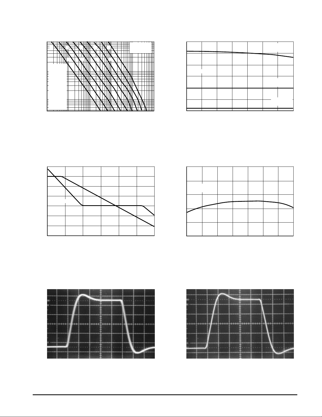
Figure 1. Timing Resistor versus
100 k
1
3
Ω
CT=
1. 100 nF
10 k
2. 47 nF
3. 22 nF
4. 10 nF
5. 4.7 nF
, TIMING RESISTOR ( )
6. 2.2 nF
T
R
7. 1.0 nF
1.0 k
8. 470 pF
9. 220 pF
470
100 1000 10
2
Oscillator Frequency
5
7
9
4
6
8
4
f
, OSCILLAT OR FREQUENCY (Hz)
osc
10
5
MC34025 MC33025
VCC = 15 V
TA = +25
6
10
°
C
7
10
1200
1000
, OSCILLAT OR FREQUENCY (kHz)f
osc
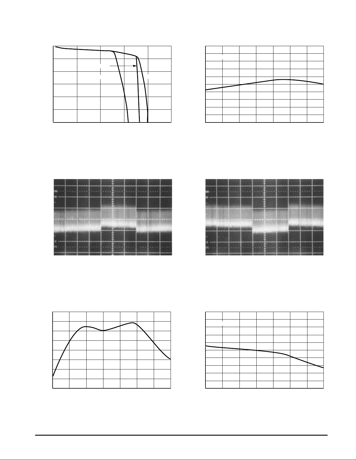
Figure 2. Oscillator Frequency versus T emperature
1.0 MHz
800
600
400
200
VCC = 15 V
400 kHz
50 kHz
0
– 55 – 25 0 25 75 100 125
TA, AMBIENT TEMPERATURE (°C)
50
RT = 1.2 k
CT = 1.0 nF
RT = 3.6 k
CT = 1.0 nF
RT = 36 k
CT = 1.0 nF
Figure 3. Error Amp Open Loop Gain and
Phase versus Frequency
120
100
80
60
40
20
, OPEN LOOP VOL TAGE GAIN (dB)
0
VOL
A
–20
10 100 1.0 k 10 k 100 k 1.0 M 10 M
Phase
Gain
f, FREQUENCY (Hz)
Figure 5. Error Amp Small Signal
Transient Response
2.55 V
0
45
90
θ
135
1.3
1.28
C)
°
1.26
1.24
, ZERO DUTY CYCLE (V)
, EXCESS PHASE (
th
1.22
V
1.2
3.0 V
Figure 4. PWM Comparator Zero Duty Cycle
Threshold V oltage versus Temperature
VCC = 15 V
Pin 7(9) = 0 V
–55 –25 0 25 50 75 100
TA, AMBIENT TEMPERATURE (
°
C)
Figure 6. Error Amp Large Signal
Transient Response
125
2.5 V
2.45 V
4
2.5 V
2.0 V
0.1 µs/DIV 0.1 µs/DIV
MOTOROLA ANALOG IC DEVICE DATA
MC34025 MC33025
Figure 7. Reference V oltage Change
0
–5.0
VCC = 15 V
–10
–15
–20
–25
, REFERENCE VOLTAGE CHANGE (mV)
ref
V
–30
0
10 20 30 40 50
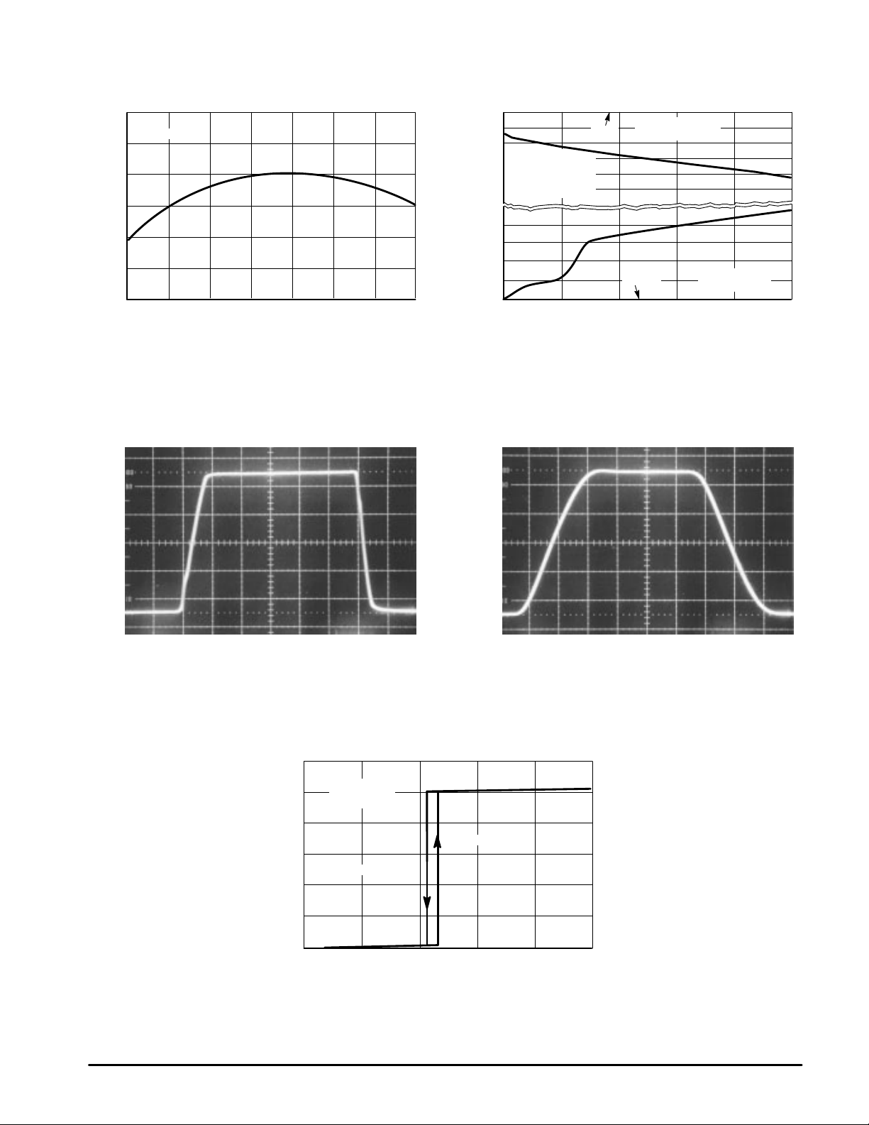
Figure 9. Reference Line Regulation Figure 10. Reference Load Regulation
versus Source Current
TA = –55°C
TA = +125°C
I
, SOURCE CURRENT (mA)
Source
TA = +25°C
65.6
65.2
64.8
64.4
, REFERENCE SHORT CIRCUIT CURRENT (mA)
SC
I
Figure 8. Reference Short Circuit Current
versus T emperature
66
VCC = 15 V
64
–55
–25 0 25 50 75 100 125
TA, AMBIENT TEMPERATURE (
°
C)
2.0 mV/DIV
V
LINE REGULA TION 10 V – 24 V
ref
2.0 ms/DIV
Figure 11. Current Limit Comparator Threshold
Change versus T emperature
4.0
2.0
0
–2.0
–4.0
–6.0
–8.0
–10
–12
(CL), CURRENT LIMIT THRESHOLD CHANGE (mV)V
th
∆
TA, AMBIENT TEMPERATURE (°C)
2.0 mV/DIV
V
ref
Figure 12. Shutdown Comparator Threshold
V oltage versus Temperature
1.50
VCC = 15 V
1.46
1.42
1.38
1.34
, SHUTDOWN THRESHOLD VOLTAGE (V)V
th
1.30
100 0
–55 –25 25 50 75 100 125–50 – 25 0 25 50 75 125
TA, AMBIENT TEMPERATURE (
LINE REGULA TION 1.0 mA – 10 mA
2.0 ms/DIV
°
C)
MOTOROLA ANALOG IC DEVICE DATA
5
MC34025 MC33025
Figure 13. Soft–Start Charge Current
versus T emperature
A)
10
µ
, SOFT-ST ART CHARGE CURRENT (
I
chg
VCC = 15 V
9.5
9.0
8.5
8.0
7.5
7.0
–55 –25 0 25 50 75 100 125
TA, AMBIENT TEMPERATURE (
°
C)
, OUTPUT SA TURATION VOLTAGE (V)
sat
V
0
–1.0
–2.0
2.0
1.0
0
Figure 14. Output Saturation Voltage
versus Load Current
Source Saturation
V
CC
(Load to Ground)
VCC = 15 V
µ
s Pulsed Load
80
120 Hz Rate
°
TA = +25
0 0.2 0.4 0.6 0.8 1.0
C
Ground
IO, OUTPUT LOAD CURRENT (A)
Figure 15. Drive Output Rise and Fall Time Figure 16. Drive Output Rise and Fall Time
Sink Saturation
(Load to VCC)
OUTPUT RISE & FALL TIME 1.0 nF LOAD
50 ns/DIV
Figure 17. Supply V oltage versus Supply Current
30
RT = 3.65 k
25
20
15
10
, SUPPLY CURRENT (mA)
CC
5.0
I
CT = 1.0 nF
VCC Decreasing
0
0 4.0 8.0 12 16 20
OUTPUT RISE & FALL TIME 10.0 nF LOAD
50 ns/DIV
Ω
VCC Increasing
VCC, SUPPLY VOLT AGE (V)
6
MOTOROLA ANALOG IC DEVICE DATA
MC34025 MC33025
16
V
ref
4
Clock
5
R
T
C
T
Error Amp Output
Noninverting Input
Inverting Input
Soft–Start
Ramp
C
SS
6
1.25 V
7
3
Error
Amp
2
1
8
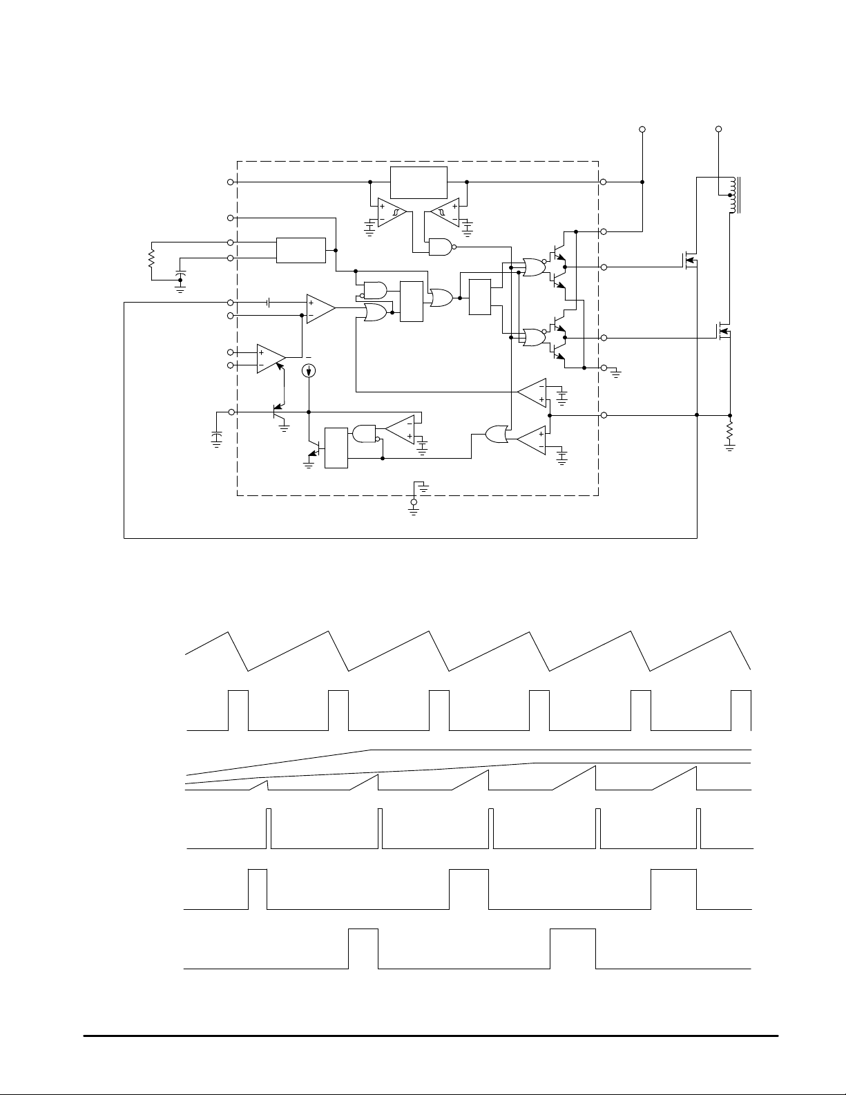
Figure 18. Representative Block Diagram
Reference
Regulator
4.2 V
V
ref
Oscillator
PWM
Comparator
+
9.0
µ
R
Q
S
UVLO
PWM Latch
A
Soft–Start Latch
R
Q
S
Steering
Flip Flop
0.5 V
UVLO
9.2 V
Q
T
Q
V
CC
Current
Limit
Shutdown
1.0 V
1.4 V
V
CC
15
V
CC
13
V
C
14
Output B
11
Output A
12
Power Ground
9
Current Limit/
Shutdown
V
in
C
T
Clock
Soft–Start
Error Amp Output
Ramp
PWM
Comparator
10
Ground
Figure 19. Current Limit Operating Waveforms
Output A
Output B
MOTOROLA ANALOG IC DEVICE DATA
7

MC34025 MC33025
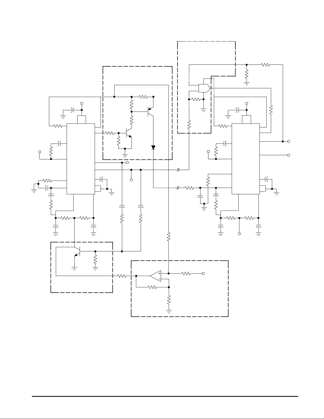
OPERA TING DESCRIPTION
The MC33025 and MC34025 series are high speed, fixed
frequency, double–ended pulse width modulator controllers
optimized for high frequency operation. They are specifically
designed for Off–Line and DC–to–DC converter applications
offering the designer a cost effective solution with minimal
external components. A representative block diagram is
shown in Figure 18.
Oscillator
The oscillator frequency is programmed by the values
selected for the timing components RT and CT. The RT pin is
set to a temperature compensated 3.0 V. By selecting the
value of RT, the charge current is set through a current mirror
for the timing capacitor CT. This charge current runs
continuously through CT. The discharge current is ratioed to
be 10 times the charge current, which yields the maximum
duty cycle of 90%. CT is charged to 2.8 V and discharged to
1.0 V . During the discharge of CT, the oscillator generates an
internal blanking pulse that resets the PWM Latch, inhibits
the outputs, and toggles the steering flip–flop. The threshold
voltages on the oscillator comparator is trimmed to guarantee
an oscillator accuracy of 5.0% at 25°C.
Additional dead time can be added by externally
increasing the charge current to CT as shown in Figure 23.
This changes the charge to discharge ratio of CT which is set
internally to I
ratio will be:
% Deadtime
A bidirectional clock pin is provided for synchronization or
for master/slave operation. As a master, the clock pin
provides a positive output pulse during the discharge of CT.
As a slave, the clock pin is an input that resets the PWM latch
and blanks the drive output, but does not discharge CT.
Therefore, the oscillator is not synchronized by driving the
clock pin alone. Figures 29 and 30 provide suggested
synchronization.
Error Amplifier
A fully compensated Error Amplifier is provided. It features
a typical DC voltage gain of 95 dB and a gain bandwidth
product of 8.3 MHz with 75 degrees of phase margin
(Figure 3). Typical application circuits will have the
noninverting input tied to the reference. The inverting input
will typically be connected to a feedback voltage generated
from the output of the switching power supply. Both inputs
have a Common Mode Voltage (VCM) input range of 1.5 V to
5.5 V . The Error Amplifier Output is provided for external loop
compensation.
Soft–Start Latch
Soft–Start is accomplished in conjunction with an external
capacitor. The soft start capacitor is charged by an internal
9.0 µA current source. This capacitor clamps the output of
the error amplifier to less than its normal output voltage, thus
limiting the duty cycle.
charge
/10 I
charge
I
+
. The new charge to discharge
)
I
10 (I
l
charge
charge
)
additiona
The time it takes for a capacitor to reach full charge is
given by:
t[(4.5 • 105)C
A Soft–Start latch is incorporated to prevent erratic
operation of this circuitry. Two conditions can cause the
Soft–Start circuit to latch so that the Soft–Start capacitor
stays discharged. The first condition is activation of an
undervoltage lockout of either VCC or V
condition is when current sense input exceeds 1.4 V. Since
this latch is “set dominant”, it cannot be reset until either of
these signals is removed, and the voltage at C
than 0.5 V.
PWM Comparator and Latch
A PWM circuit typically compares an error voltage with a
ramp signal. The outcome of this comparison determines the
state of the output. In voltage mode operation the ramp signal
is the voltage ramp of the timing capacitor. In current mode
operation the ramp signal is the voltage ramp induced in a
current sensing element. The ramp input of the PWM
comparator is pinned out so that the user can decide which
mode of operation best suits the application requirements.
The ramp input has a 1.25 V offset such that whenever the
voltage at this pin exceeds the Error Amplifier Output voltage
minus 1.25 V , the PWM comparator will cause the PWM latch
to set, disabling the outputs. Once the PWM latch is set, only
a blanking pulse by the oscillator can reset it, thus initiating
the next cycle.
A toggle flip flop connected to the output of the PWM latch
controls which output is active. The flip flop is pulsed by an
OR gate that gets its inputs from the oscillator clock and the
output of the PWM latch. A pulse from either one will cause
the flip flop to enable the other output.
Current Limiting and Shutdown
A pin is provided to perform current limiting and shutdown
operations. Two comparators are connected to the input of
this pin. When the voltage at this pin exceeds 1.0 V, one of
the comparators is activated. The output of this comparator
sets the PWM latch, which disables the output. In this way
cycle–by–cycle current limiting is accomplished. If a current
limit resistor is used in series with the power devices, the
value of the resistor is found by:
R
If the voltage at this pin exceeds 1.4 V, the second
comparator is activated. This comparator sets a latch which,
in turn, causes the Soft–Start capacitor to be discharged. In
this way a “hiccup” mode of recovery is possible in the case
of output short circuits. If a current limit resistor is used in
series with the output devices, the peak current at which the
controller will enter a “hiccup” mode is given by:
I
+
Sense
shutdown
Soft-Start
1.0 V
I
pk (switch)
1.4 V
+
R
Sense
. The second
ref
Soft–Start
is less
8
MOTOROLA ANALOG IC DEVICE DATA

MC34025 MC33025
Undervoltage Lockout
There are two undervoltage lockout circuits within the IC.
The first senses VCC and the second V
VCC must exceed 9.2 V and V
the outputs can be enabled and the Soft–Start latch released.
If VCC falls below 8.4 V or V
are disabled and the Soft–Start latch is activated. When the
UVLO is active, the part is in a low current standby mode
allowing the IC to have an off–line bootstrap start–up circuit.
Typical start–up current is 500 µA.
Output
The MC34025 has two high current totem pole outputs
specifically designed for direct drive of power MOSFETs.
They are capable of up to ± 2.0 A peak drive current with a
typical rise and fall time of 30 ns driving a 1.0 nF load.
Separate pins for VC and Power Ground are provided.
With proper implementation, a significant reduction of
switching transient noise imposed on the control circuitry is
possible. The separate VC supply input also allows the
designer added flexibility in tailoring the drive voltage
independent of VCC.
Reference
A 5.1 V bandgap reference is pinned out and is trimmed to
an initial accuracy of ±1.0% at 25°C. This reference has short
circuit protection and can source in excess of 10 mA for
powering additional control system circuitry.
Design Considerations
Do not attempt to construct the converter on
wire–wrap or plug–in prototype boards. With high
frequency, high power, switching power supplies it is
imperative to have separate current loops for the signal paths
and for the power paths. The printed circuit layout should
contain a ground plane with low current signal and high
current switch and output grounds returning on separate
paths back to the input filter capacitor. All bypass capacitors
and snubbers should be connected as close as possible to
the specific part in question. The PC board lead lengths must
be less than 0.5 inches for effective bypassing or snubbing.
must exceed 4.2 V before
ref
falls below 3.6 V, the outputs
ref
. During power–up,
ref
Instabilities
In current mode control, an instability can be encountered
at any given duty cycle. The instability is caused by the
current feedback loop. It has been shown that the instability is
caused by a double pole at half the switching frequency . If an
external ramp (Se) is added to the on–time ramp (Sn) of the
current–sense waveform, stability can be achieved (see
Figure 20).
One must be careful not to add too much ramp
compensation. If too much is added, the system will start to
perform like a voltage mode regulator. All benefits of current
mode control will be lost. Figures 28A and 28B show
examples of two different ways in which external ramp
compensation can be implemented.
Figure 20. Ramp Compensation
Ramp Input
Ramp Compensation
S
e
A simple equation can be used to calculate the amount of
external ramp necessary to add that will achieve stability in
the current loop. For the following equations, the calculated
values for the application circuit in Figure 36 are also shown.
V
Se+
NP, N
V
O
= number of power transformer primary
S
= or secondary turns
A
= gain of the current sense network
i
= (see Figures 25, 26 and 27)
L
= output inductor
R
= current sense resistance
S
where: = DC output voltage
+
+
Current Signal
S
n
N
O
S
ǒ
Ǔ
N
L
P
(R
1.25 V
)
A
S
i
MOTOROLA ANALOG IC DEVICE DATA
For the application circuit:
Se+
+
5
4
ǒ
Ǔ
16
1.8 µ
0.115 Vńµs
(
0.3)(0.55
)
9

MC34025 MC33025
PIN FUNCTION DESCRIPTION
Pin No.
DIP/SOIC
1 Error Amp
2 Error Amp
3 Error Amp
4 Clock This is a bidirectional pin used for synchronization.
5 R
6 C
7 Ramp Input For voltage mode operation this pin is connected to CT. For current mode operation this pin is
8 Soft–Start A capacitor at this pin sets the Soft–Start time.
9 Current
10 Ground This pin is the ground for the control circuitry.
11 Output A This is a high current totem pole output.
12 Power Ground This is a separate power ground return that is connected back to the power source. It is used to
13 V
14 Output B This is a high current totem pole output.
15 V
16 V
Function Description
Inverting
Input
Noninverting
Input
Output
T
T
Limit/Shutdown
C
CC
ref
This pin is usually used for feedback from the output of the power supply.
This pin is used to provide a reference in which an error signal can be produced on the output of the
error amp. Usually this is connected to V
be used.
This pin is provided for compensating the error amp for poles and zeros encountered in the power
supply system, mostly the output LC filter.
The value of RT sets the charge current through timing Capacitor, CT.
In conjunction with RT, the timing Capacitor sets the switching frequency. Because this part is a
push–pull output, each output runs at one–half the frequency set at this pin.
connected through a filter to the current sensing element.
This pin has two functions. First, it provides cycle–by–cycle current limiting. Second, if the
current is excessive, this pin will reinitiate a Soft–Start cycle.
reduce the effects of switching transient noise on the control circuitry .
This is a separate power source connection for the outputs that is connected back to the power source
input. With a separate power source connection, it can reduce the effects of switching transient noise
on the control circuitry.
This pin is the positive supply of the control IC.
This is a 5.1 V reference. It is usually connected to the noninverting input of the error amplifier.
, however an external reference can also
ref
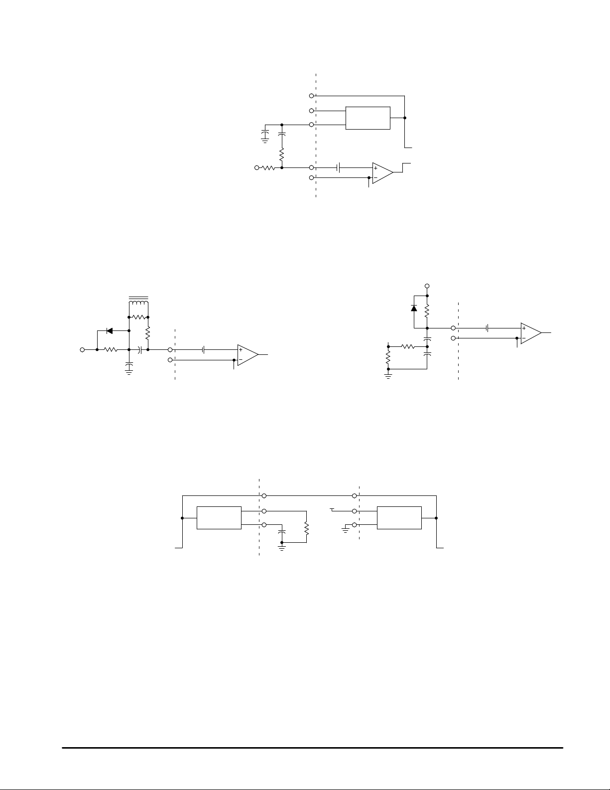
Figure 21. V oltage Mode Operation
4
5
Oscillator
C
T
Output Voltage
Feedback Input
In voltage mode operation, the control range on the output of the Error
Amplifier from 0% to 90% duty cycle is from 2.25 V to 4.05 V.
6
1.25 V
7
3
1
2
V
ref
10
Figure 22. Current Mode Operation
4
5
Oscillator
C
From Current
Sense Element
Output Voltage
Feedback Input
In current mode control, an RC filter should be placed at the ramp input to filter
the leading edge spike caused by turn–on of a power MOSFET.
6
T
1.25 V
7
3
1
2
V
ref
MOTOROLA ANALOG IC DEVICE DATA

MC34025 MC33025
Figure 23. Dead Time Addition
V
ref
R
DT
4
5
R
6
T
Additional dead time can be added by the addition of a dead time resistor from
V
to CT. See text on oscillator section for more information.
ref
C
T
Oscillator
Figure 25. Resistive Current Sensing
Figure 24. External Clock Synchronization
5.0 V
0 V
R
T
The sync pulse fed into the clock pin must be at least 3.9 V . RT and CT need
to be set 10% slower than the sync frequency. This circuit is also used in voltage
mode operation for master/slave operation. The clock signal would be coming
from the master which is set at the desired operating frequency, while the slave
is set 10% slower.
4
5
6
C
T
Oscillator
The addition of an RC filter will eliminate instability caused by the leading edge spike
on the current waveform. This sense signal can also be used at the ramp input pin for
current mode control. For ramp compensation it is necessary to know the gain of the
current feedback loop. If a transformer is used, the gain can be calculated by:
Figure 26. Primary Side Current Sensing
9
R
w
I
Sense
A
+
i
9
R
Sense
turns ratio
I
Sense
Figure 27. Primary or Secondary Side
Current Sensing
9
R
w
0
I
Sense
The addition of an RC filter will eliminate instability caused by the leading edge spike on the current waveform. This sense signal can also be used at the ramp input
pin for current mode control. For ramp compensation it is necessary to know the gain of the current feedback loop. The gain can be calculated by:
R
+
w
turns ratio
A
i
MOTOROLA ANALOG IC DEVICE DATA
11
MC34025 MC33025
Figure 28A. Slope Compensation (Noise Sensitive)
4
5
6
C
T
C
1
Oscillator
R
Current Sense
Information
This method of slope compensation is easy to implement, however, it is noise sensitive. Capacitor C1 provides AC coupling. The oscillator signal is added to the
current signal by a voltage divider consisting of resistors R1 and R2.
1
R
2
1.25 V
7
3
Figure 28B. Slope Compensation (Noise Immune)
R
Output
C
M
f
Ramp
Input
R
M
C
f
1.25 V
7
3
Current Sense
Transformer
R
w
R
Output
When only one output is used, this method of slope compensation can be used and it is relatively noise immune. Resistor RM and capacitor CM provide the added
slope necessary. By choosing RM and CM with a larger time constant than the switching frequency, you can assume that its charge is linear. First choose CM, then R
can be adjusted to achieve the required slope. The diode provides a reset pulse at the ramp input at the end of every cycle. The charge current IM can be calculated
by IM = CMSe. Then RM can be calculated by RM = VCC/IM.
R
M
C
f
C
f
M
Figure 28. Keeps Fig numbering sequence correct
Ramp
Input
1.25 V
7
3
Current Sense
Resistor
M
Figure 29. Current Mode Master/Slave Operation Over Short Distances
4
V
ref
5
6
Oscillator
Oscillator
4
5
6
R
T
C
T
12
MOTOROLA ANALOG IC DEVICE DATA
MC34025 MC33025
Figure 30. Synchronization Over Long Distances
Synchronizes Both
Converters
to the Same Phase
10 k
22 k
470 pF
+15 V
15
2
3
1
5
6
79
MC34025
13
11
14
8
12
10
16
4
2200
Synchronizes Both Converters
to the Same Operating Frequency
20
1.0 k
MMBT3906
4700
MMBT3904
430
562
MMBD914
Output A
Output B
680 pF680 pF
562
4.7 k
10 k
21
470 pF
30 k
4.7 k
+15 V
3.0 k
15
2
3
FBFB
1
5
6
79
MC34025
13
16
4
11
Output A
14
Output B
8
12
10
MMBT3904
Provides Leading
Edge Blanking
100
MC34071
3320
1.0 k
100 k
1.0 k
Provides Current
Sense Amplification &
Eliminates Leading
Edge Spike
From Curr
Sense
From Curr
Sense
MOTOROLA ANALOG IC DEVICE DATA
13

MC34025 MC33025
Figure 31. Buffered Maximum Clamp Level
1
2
V
ref
R
1
R
2
In voltage mode operation, the maximum duty cycle can be clamped. By the
addition of a PNP transistor to buffer the clamp voltage, the Soft–Start current
is not affected by R1.
The new equation for Soft–Start is
In current mode operation, this circuit will limit the maximum voltage allowed
at the ramp input to end a cycle.
8
C
SS
V
clamp
t
[
)
9.0 µA
+
0.6
ǒ
Ǔ
C
SS
Figure 33. Isolated MOSFET Drive
V
C
15
Isolation
Boundary
14
Figure 32. Bipolar Transistor Drive
I
B
+
15
V
C
V
in
0
–
Base Charge
Removal
14
Q
T
Q
11
12
The totem pole output can furnish negative base current for enhanced
transistor turn–off, with the addition of the capacitor in series with the base.
To Current
Sense Input
R
S
Figure 34. Direct Transformer Drive
V
C
15
14
Q
T
Q
11
12
The totem pole output can easily drive pulse transformers. A Schottky diode is recommended when driving inductive loads at high frequencies. The diode can reduce
the driver’s power dissipation due to excessive ringing, by preventing the output pin from being driven below ground.
Q
T
Q
V
C
11
12
Figure 35. MOSFET Parasitic Oscillations
V
C
15
14
Q
T
Q
11
V
in
A series gate resistor may be needed to damp high frequency parasitic
oscillation caused by a MOSFET’s input capacitance and any series wiring
inductance in the gate–source circuit. The series resistor will also decrease the
MOSFET’s switching speed. A Schottky diode can reduce the driver’s power
dissipation due to excessive ringing, by preventing the output pin from being
driven below ground. The Schottky diode also prevents substrate injection
when the output pin is driven below ground.
14
12
To Current
Sense Input
R
S
MOTOROLA ANALOG IC DEVICE DATA
MC34025 MC33025
36 V to 56 V
in
V
47 k
1N5819
100
47
1500 pF
22
4.7
15
5.0 V
O
V
2
L
900 nH
1
µ
1
L
1.8 H
MBR2535CTL
1
T
10
10
13
3
µ
2.0 F
µ
10 F
50
IRF640
4.7
14
1500 pF
22
1N5819
1600 pF
1N5819
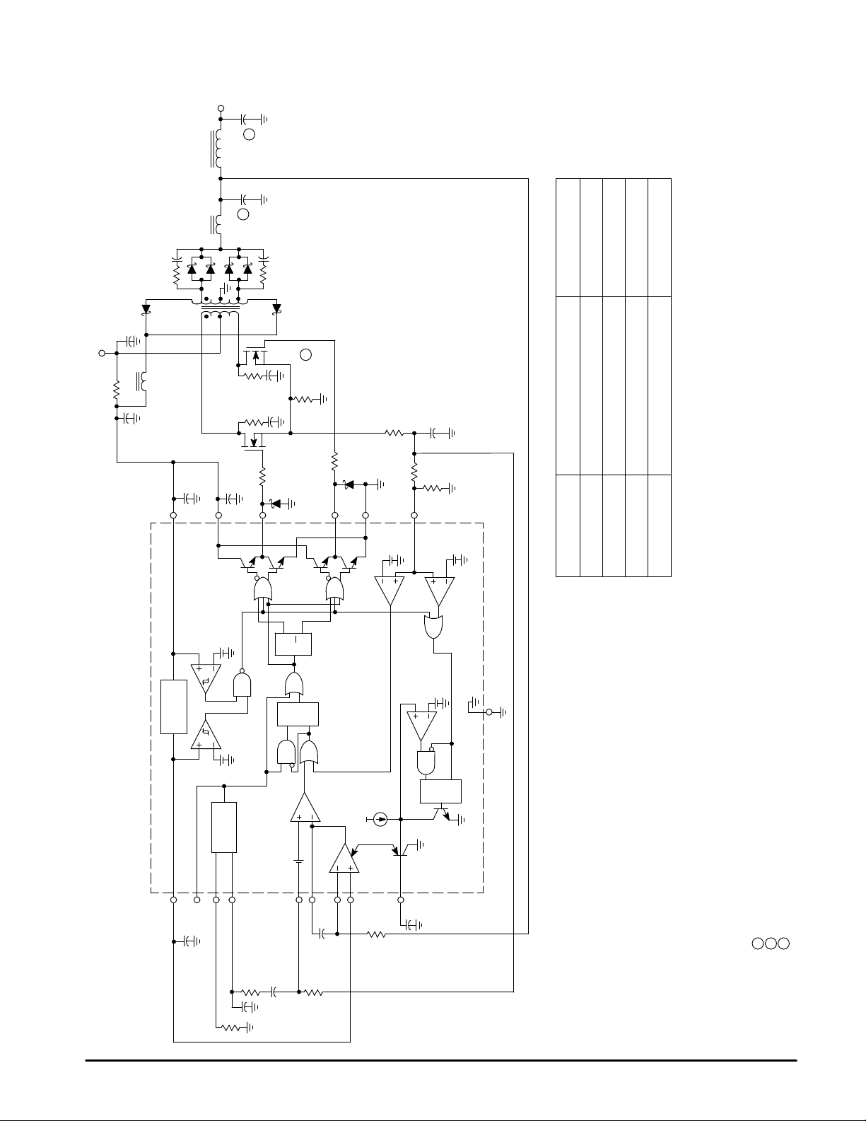
Figure 36. Keeps Fig numbering sequence correct
2
Ω
0.3
220 pF
100
4.7
11
1N5819
12
100
9
1.0 V
47
1.4 V
±
±
54 mV = 1.0%
14 mV = 0.275%
in O
in O
V = 40 V to 56 V, I = 15 A
V = 48 V, I = 8.0 V to 15 A
Test Condition Result
Line Regulation
Load Regulation
50 mVp–p
71.2%
in O
in O
V = 48 V, I = 15 A
V = 48 V, I = 15 A
Output Ripple
Efficiency
Figure 36. Application Circuit
Regulator
Reference
4
16
1.0
9.2 V
4.0 V
5
1.2 k
Oscillator
6
22 k
1000 pF
Q
0.01
Q
T
Q
R
1.25 V
7
3
S
PWM Latch
2
µ
0.015 F
2.0 k
Limit
Current
µ
9.0 A
Error
Amp
1
47 k
Shutdown
0.5 V
10
R
S
Q
8
µ
0.01
Primary: 16 turns center tapped #48 A WG (1300 strands litz wire)
Secondary: 4 turns center tapped 0.003” (2 layers) copper foil
Bootstrap: 1 turn added to each secondary output #36 A WG
Core: Philips 3F3, part #4312 020 4124
Bobbin: Philips part #4322 021 3525
Coilcraft P3269–A
2 turns #48 A WG (1300 strands litz wire)
Core: Philips 3F3, part #EP10–3F3
Bobbin: Philips part #EP10PCB1–8
L = 1.8 H
–
1
T
–
1
L
Coilcraft P3270–A
Power FET : AAVID Heatsink #533902B02554 with clip
7 turns #18 AWG, 1/2” diameter air core
Coilcraft P3271–A
–
2
L
Heatsinks –
µ
Ω
µ
All power devices are insulated with Berquist Sil–Pad 1500
Output Rectifiers: AA VID Heatsink #533402B02552 with clip
5 (1.5 ) resistors in parallel
2 (1.0 F) cearmic capacitors in parallel
10 (1.0 F) ceramic capacitors in parallel
–
–
–
2
3
1
Insulators –
MOTOROLA ANALOG IC DEVICE DATA
15

100 pF
1000 pF
0.01
100 pF
0.01
MC34025 MC33025
Figure 37. PC Board With Components
4.7 Hµ
1N5819
1N5819
2535CTI
MBR
1
+
1N5819
+
10
1N5819
2535CTI
2200 pF
MBR
1500 pF
1500 pF
4.0
″
6.5
″
(Top View)
1
1
16
MOTOROLA ANALOG IC DEVICE DATA

MC34025 MC33025
Figure 38. PC Board Without Components
(Top View)
4.0
″
MOTOROLA ANALOG IC DEVICE DATA
6.5
″
(Bottom View)
17

MC34025 MC33025
OUTLINE DIMENSIONS
P SUFFIX
PLASTIC PACKAGE
CASE 648–08
–A–
916
B
18
F
C
S
–T–
H
G
D
16 PL
K
M M
TA0.25 (0.010)
–A–
916
–B–
P 8 PL
18
G 14 PL
0.25 (0.010)
J
F
C
–T–
SEATING
K
16 PL
D
0.25 (0.010) T A B
M
PLANE
S S
L
SEATING
PLANE
J
DW SUFFIX
PLASTIC PACKAGE
CASE 751G–02
(SO–16L)
M M
B
R
X 45°
M
NOTES:
1. DIMENSIONING AND TOLERANCING PER ANSI
Y14.5M, 1982.
2. CONTROLLING DIMENSION: INCH.
3. DIMENSION L TO CENTER OF LEADS WHEN
FORMED PARALLEL.
4. DIMENSION B DOES NOT INCLUDE MOLD FLASH.
5. ROUNDED CORNERS OPTIONAL.
INCHES MILLIMETERS
MIN MINMAX MAX
DIM
A
0.740
B
0.250
C
0.145
D
0.015
F
0.040
G
0.100 BSC
H
M
NOTES:
1. DIMENSIONING AND TOLERANCING PER
2. CONTROLLING DIMENSION: MILLIMETER.
3. DIMENSIONS A AND B DO NOT INCLUDE
4. MAXIMUM MOLD PROTRUSION 0.15 (0.006)
5. DIMENSION D DOES NOT INCLUDE
0.050 BSC
J
0.008
K
0.110
L
0.295
M
0
°
S
0.020
ANSI Y14.5M, 1982.
MOLD PROTRUSION.
PER SIDE.
DAMBAR PROTRUSION. ALLOWABLE
DAMBAR PROTRUSION SHALL BE 0.13
(0.005) TOTAL IN EXCESS OF D DIMENSION
AT MAXIMUM MATERIAL CONDITION.
INCHES
MIN MAXMAX
DIM
0.400
A
0.292
B
0.093
C
0.014
D
0.020
F
0.050 BSC
G
J
0.010
K
0.004
M
0
°
P
0.395
R
0.010
0.770
0.270
0.175
0.021
0.070
0.015
0.130
0.305
10
0.040
0.411
0.299
0.104
0.019
0.035
0.012
0.009
7
0.415
0.029
°
°
18.80
19.55
6.35
6.85
3.69
4.44
0.39
0.53
1.02
1.77
2.54 BSC
1.27 BSC
0.21
0.38
2.80
3.30
7.50
7.74
0
10
°
°
0.51
1.01
MILLIMETERS
MIN MAX
10.15
10.45
7.40
7.60
2.35
2.65
0.35
0.49
0.50
0.90
1.27 BSC
0.25
0.32
0.10
0.25
0
7
°
°
10.05
10.55
0.25
0.75
18
MOTOROLA ANALOG IC DEVICE DATA

MC34025 MC33025
OUTLINE DIMENSIONS
FN SUFFIX
PLASTIC PACKAGE
CASE 775–02
(PLCC)
–L–
20
C
0.010 (0.250) T L
–N–
Y BRK
B
0.007 (0.180) T L
D
U
0.007 (0.180) T L
–M
SNSM
SNSM
–M
–M–
W
1
D
V
Z
G1
X
0.010 (0.250) T L
–M
SNSS
VIEW D–D
A
0.007 (0.180) T L
–M
SNSM
Z
G1
R
0.007 (0.180) T L
E
0.004 (0.100)
G
J
–T–
SEATING
PLANE
VIEW S
SNSS
–M
–M
SNSM
0.007 (0.180) T L
H
–M
SNSM
K1
K
F
0.007 (0.180) T L
–M
SNSM
VIEW S
NOTES:
1. DATUMS –L–, –M–, AND –N– DETERMINED WHERE
TOP OF LEAD SHOULDER EXITS PLASTIC BODY
AT MOLD PARTING LINE.
2. DIM G1, TRUE POSITION TO BE MEASURED AT
DATUM –T–, SEATING PLANE.
3. DIM R AND U DO NOT INCLUDE MOLD FLASH.
ALLOWABLE MOLD FLASH IS 0.010 (0.250) PER
SIDE.
4. DIMENSIONING AND TOLERANCING PER ANSI
Y14.5M, 1982.
5. CONTROLLING DIMENSION: INCH.
6. THE PACKAGE TOP MAY BE SMALLER THAN THE
PACKAGE BOTTOM BY UP TO 0.012 (0.300).
DIMENSIONS R AND U ARE DETERMINED AT THE
OUTERMOST EXTREMES OF THE PLASTIC BODY
EXCLUSIVE OF MOLD FLASH, TIE BAR BURRS,
GATE BURRS AND INTERLEAD FLASH, BUT
INCLUDING ANY MISMATCH BETWEEN THE TOP
AND BOTTOM OF THE PLASTIC BODY.
7. DIMENSION H DOES NOT INCLUDE DAMBAR
PROTRUSION OR INTRUSION. THE DAMBAR
PROTRUSION(S) SHALL NOT CAUSE THE H
DIMENSION TO BE GREATER THAN 0.037 (0.940).
THE DAMBAR INTRUSION(S) SHALL NOT CAUSE
THE H DIMENSION TO BE SMALLER THAN 0.025
(0.635).
INCHES MILLIMETERS
MIN MINMAX MAX
DIM
A
0.385
0.385
0.165
0.090
0.013
0.026
0.020
0.025
0.350
0.350
0.042
0.042
0.042
—
2
0.310
0.040
0.395
0.395
0.180
0.110
0.019
0.032
—
—
0.356
0.356
0.048
0.048
0.056
0.020
°
10
0.330
—
G1
K1
B
C
E
F
G
H
J
K
R
U
V
W
X
Y
Z
9.78
10.03
9.78
10.03
4.20
4.57
2.29
2.79
0.33
0.48
1.27 BSC0.050 BSC
0.66
0.81
0.51
—
0.64
—
8.89
9.04
8.89
9.04
1.07
1.21
1.07
1.21
1.07
1.42
—
0.50
°
2
7.88
1.02
10
8.38
—
°
°
MOTOROLA ANALOG IC DEVICE DATA
19

MC34025 MC33025
Motorola reserves the right to make changes without further notice to any products herein. Motorola makes no warranty , representation or guarantee regarding
the suitability of its products for any particular purpose, nor does Motorola assume any liability arising out of the application or use of any product or circuit, and
specifically disclaims any and all liability, including without limitation consequential or incidental damages. “T ypical” parameters which may be provided in Motorola
data sheets and/or specifications can and do vary in different applications and actual performance may vary over time. All operating parameters, including “Typicals”
must be validated for each customer application by customer’s technical experts. Motorola does not convey any license under its patent rights nor the rights of
others. Motorola products are not designed, intended, or authorized for use as components in systems intended for surgical implant into the body, or other
applications intended to support or sustain life, or for any other application in which the failure of the Motorola product could create a situation where personal injury
or death may occur. Should Buyer purchase or use Motorola products for any such unintended or unauthorized application, Buyer shall indemnify and hold Motorola
and its officers, employees, subsidiaries, affiliates, and distributors harmless against all claims, costs, damages, and expenses, and reasonable attorney fees
arising out of, directly or indirectly, any claim of personal injury or death associated with such unintended or unauthorized use, even if such claim alleges that
Motorola was negligent regarding the design or manufacture of the part. Motorola and are registered trademarks of Motorola, Inc. Motorola, Inc. is an Equal
Opportunity/Affirmative Action Employer.
How to reach us:
USA/EUROPE/Locations Not Listed: Motorola Literature Distribution; JAP AN: Nippon Motorola Ltd.: SPD, Strategic Planning Office, 4–32–1,
P.O. Box 5405, Denver, Colorado 80217. 303–675–2140 or 1–800–441–2447 Nishi–Gotanda, Shinagawa–ku, Tokyo 141, Japan. 81–3–5487–8488
Mfax: RMFAX0@email.sps.mot.com – TOUCHTONE 602–244–6609 ASIA/P ACIFIC: Motorola Semiconductors H.K. Ltd.; 8B Tai Ping Industrial Park,
INTERNET: http://motorola.com/sps
20
– US & Canada ONLY 1–800–774–1848 51 Ting Kok Road, Tai Po, N.T., Hong Kong. 852–26629298
◊
MOTOROLA ANALOG IC DEVICE DATA
Mfax is a trademark of Motorola, Inc.
MC34025/D
 Loading...