

Motorola MC34017D, MC34017P Datasheet
1
AC1
RO1
RO2
AC2
RI
RG
RC
RS
2
3
4
8
7
6
5
Device
Operating
Temperature Range
Package
SEMICONDUCTOR
TECHNICAL DATA
TELEPHONE TONE RINGER
ORDERING INFORMATION
MC34017D
MC34017P
TA = –20° to +60°C
SOIC
Plastic DIP
P SUFFIX
PLASTIC PACKAGE
CASE 626
8
1
PIN CONNECTIONS
Order this document by MC34017/D
1
8
D SUFFIX
PLASTIC PACKAGE
CASE 751
(Top View)
BIPOLAR LINEAR/I2L
1
MOTOROLA ANALOG IC DEVICE DATA
Bipolar Linear/I2L
• Complete Telephone Bell Replacement Circuit with Minimum
External Components
• On–Chip Diode Bridge and Transient Protection
• Direct Drive for Piezoelectric Transducers
• Push Pull Output Stage for Greater Output Power Capability
• Base Frequency Options – MC34017–1: 1.0 kHz
– MC34017–2: 2.0 kHz
– MC34017–3: 500 Hz
• Input Impedance Signature Meets Bell and EIA Standards
• Rejects Rotary Dial Transients
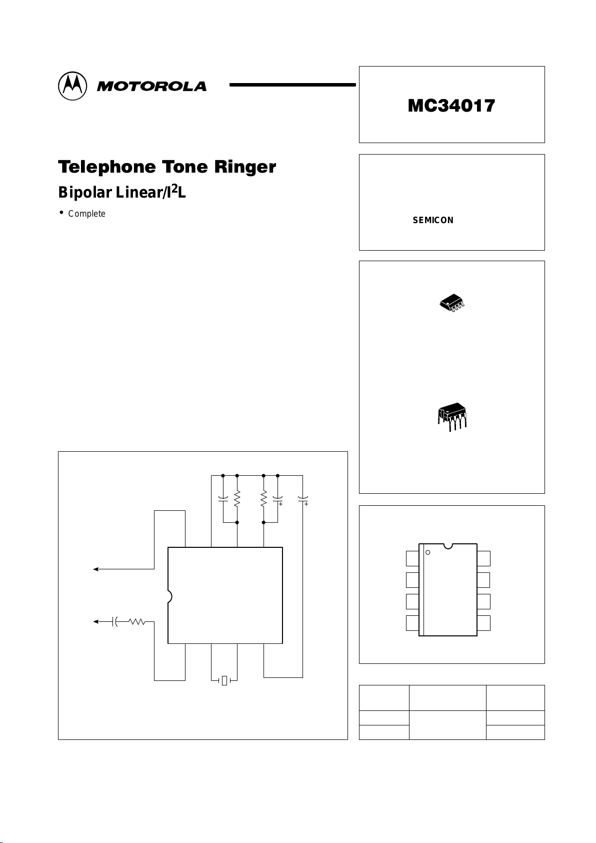
Typical Application
This device contains 97 active transistors and 79 gates.
Piezo Sound
Element
15 k
5.0 µF
25 V
2.2
µ
F
3.0 V
160 k
C
AC2 RG RC RS
AC1 RO1 RO2 RI
8765
1234
Ring
Tip
MC34017–1: C = 1000 pF
MC34017–2: C = 500 pF
MC34017–3: C = 2000 pF
MC34017–X
6.8 k
1.0
µ
F
Motorola, Inc. 1996
MC34017
2
MOTOROLA ANALOG IC DEVICE DATA
MAXIMUM RATINGS
(Voltages Referenced to RG, Pin 7)
Rating Symbol Value Unit
Operating AC Input Current (Pins 1, 8) – 20 mA, RMS
Transient Input Current (Pins 1, 8) (T<2.0 ms) V
in
±300 mA, peak
Voltage Applied at RC (Pin 6) V
RC
5.0 V
Voltage Applied at RS (Pin 5) V
RS
5.0 V
Voltage Applied to Outputs (Pins 2, 3) V
O
–2.0 to V
RI
V
Power Dissipation (@ 25°C) P
D
1.0 W
Operating Ambient Temperature T
A
–20 to +60 °C
Storage Temperature T
stg
–65 to +150 °C
NOTE: ESD data available upon request.
ELECTRICAL CHARACTERISTICS (T
A
= 25°C)
Characteristic
Test Symbol Min Typ Max Unit
Ringing Start Voltage Vdc
V
Start
= VI at Ring Start
VI > 0 1a V
Start
(+) 34 37.5 41
VI < 0 1b V
Start
(–) –34 –37.5 –41
Ringing Stop Voltage 1c V
Stop
Vdc
V
Stop
= VI at Ring Stop
MC34017–1 14 16 22
MC34017–2 12 14 20
MC34017–3 14 16 22
Output Frequencies (VI = 50 V) 1d Hz
MC34017–1 High Tone f
H
937 1010 1083
MC34017–1 Low Tone f
L
752 808 868
MC34017–1 Warble Tone f
W
11.5 12.5 14
MC34017–2 High Tone f
H
1874 2020 2166
MC34017–1 Low Tone f
L
1504 1616 1736
MC34017–1 Warble Tone f
W
11.5 12.5 14
MC34017–3 High Tone f
H
937 1010 1083
MC34017–1 Low Tone f
L
752 808 868
MC34017–1 Warble Tone f
W
23 25 28
Output Voltage (VI = 50 V) 6 V
O
34 37 43 Vpp
Output Short–Circuit Current 2 I
RO1
, I
RO2
35 60 80 mApp
Input Diode Voltage (II = 5.0 mA) 3 V
D
5.4 6.2 6.8 Vdc
Input Voltage – SCR “Of f” (II = 30 mA) 4a V
off
30 38 43 Vdc
Input Voltage – SCR “On” (II = 100 mA) 4b V
on
3.2 4.1 6.0 Vdc
RS Clamp Voltage (VI = 50 V) 5 V
clamp
1.3 1.5 1.8 Vdc
PIN FUNCTION DESCRIPTION
Pin Symbol Description
1, 8 AC1, AC2 The input terminals to the full–wave diode bridge. The ac ringing signal from the telephone line energizes the
ringer through this bridge.
5 RS The input of the threshold comparator to which diode bridge current is mirrored and sensed through an external
resistor (R3). Nominal threshold is 1.2 V . This pin internally clamps at 1.5 V.
4 RI The positive supply terminal for the oscillator, frequency divider and output buffer circuits.
2, 3 RO1, RO2 The tone ringer output terminals through which the sound element is driven.
7 RG The negative terminal of the diode bridge and the negative supply terminal of the tone generating circuitry.
6 RC The oscillator terminal for the external resistor and capacitor which control the tone ringer frequencies (R2, C2).
MC34017
3
MOTOROLA ANALOG IC DEVICE DATA
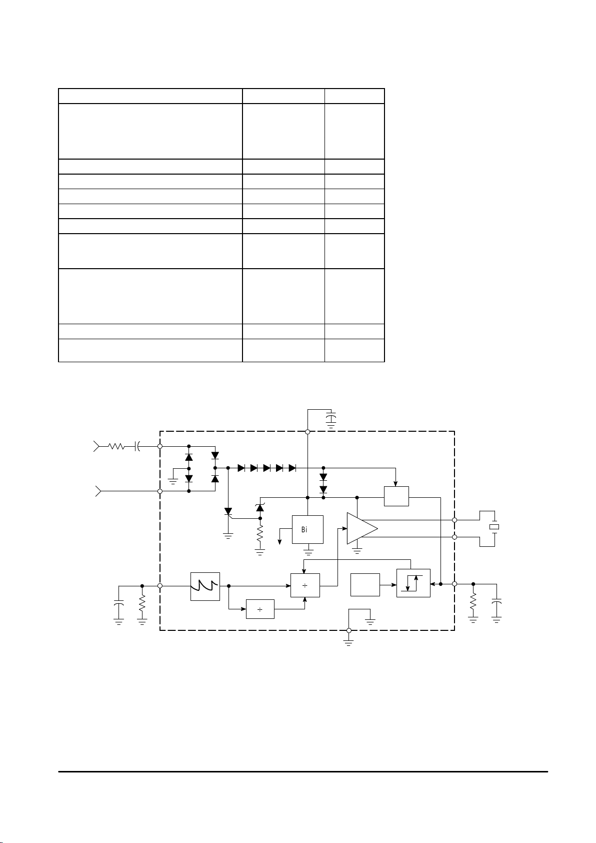
APPLICATION CIRCUIT PERFORMANCE (Refer to Typical Application)
Characteristic Typical Value Units
Output Tone Frequencies Hz
MC34017–1 808/1010
MC34017–2 1616/2020
MC34017–3 404/505
Warble Frequencies 12.5
Output Voltage (VI ≥ 60 Vrms, 20 Hz) 37 Vpp
Output Duty Cycle 50 %
Ringing Start Input Voltage (20 Hz) 36 Vrms
Ringing Stop Input Voltage (20 Hz) 21 Vrms
Maximum AC Input Voltage (≤ 68 Hz) 150 Vrms
Impedance When Ringing kΩ
VI = 40 Vrms, 15 Hz >16
VI = 130 Vrms, 23 Hz 12
Impedance When Not Ringing
VI = 10 Vrms, 24 Hz 28 kΩ
VI = 2.5 Vrms, 24 Hz >1.0 MΩ
VI = 10 Vrms, 5.0 Hz 55 kΩ
VI = 3.0 Vrms, 200 – 3200 Hz >200 kΩ
Maximum Transient Input V oltage (T ≤ 2.0 ms) 1500 V
Ringer Equivalence: Class A 0.5 –
Ringer Equivalence: Class B 0.9 –
8
C1
R1
B
B
Bias
Ref
1
6
RO1
RO2
RS
2
3
5
AC2
AC1
RC
4RI
R2C2
C3R3
22 V
Input
Current
Mirror
Push Pull
Output Buffer
C4
Threshold
Comparator
Oscillator
Tone Frequency
Divider
Warble Frequency
Divider
SCR Transient
Clamp
Diode Bridge
Ring
Piezo
Sound
Element
Tip
Block Diagram
7RG
 Loading...