

Device
Operating
Temperature Range
Package
SEMICONDUCTOR
TECHNICAL DATA
CORDLESS UNIVERSAL
TELEPHONE INTERFACE
ORDERING INFORMATION
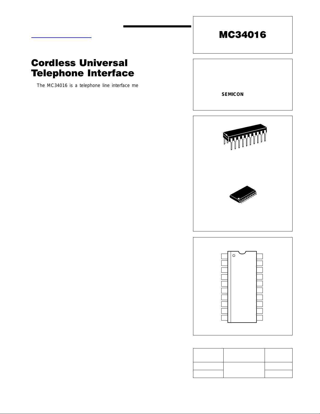
MC34016P
MC34016DW
DIP
SO–20
DW SUFFIX
PLASTIC PACKAGE
CASE 751D
20
1
(Top View)
PIN CONNECTIONS
Order this document by MC34016/D
P SUFFIX
PLASTIC PACKAGE
CASE 738
20
1
1 20
19
18
17
16
15
14
13
2
3
4
5
6
7
8
Clk
Data
Out2
Stab
Out1
BEN
LAI
AGC
T
x1
R
x1
12
9
V
CC
I
ref
R
x2
1110
HYL HYS
T
x2
SRF
LAO
Gnd
HKSW
TA = –20° to +70°C
1
MOTOROLA ANALOG IC DEVICE DATA
The MC34016 is a telephone line interface meant for use in cordless
telephone base stations for CT0, CT1, CT2 and DECT. The circuit forms the
interface towards the telephone line and performs all speech and line
interface functions like dc and ac line termination, 2–4 wire conversion,
automatic gain control and hookswitch control. Adjustment of transmission
parameters is accomplished by two 8–bit registers accessible via the
integrated serial bus interface and by external components.
• DC Masks for Voltage and Current Regulation
• Supports Passive or Active AC Set Impedance Applications
• Double Wheatstone Bridge Sidetone Architecture
• Symmetrical Inputs and Outputs with Large Signal Swing Capability
• Gain Setting and Mute Function for T
x
and Rx Amplifiers
• Very Low Noise Performance
• Serial Bus Interface SPI Compatible
• Operation from 3.0 to 5.5 V
FEATURES
Line Driver Architecture
• Two DC Masks for Voltage Regulation
• Two DC Masks for Current Regulation
• Passive or Active Set Impedance Adjustment
• Double Wheatstone Bridge Architecture
• Automatic Gain Control Function
Transmit Channel
• Symmetrical Inputs Capable of Handling Large Voltage Swing
• Gain Select Option via Serial Bus Interface
• Transmit Mute Function, Programmable via Bus
• Large Voltage Swing Capability at the Telephone Line
Receive Channel
• Double Sidetone Architecture for Optimum Line Matching
• Symmetrical Outputs Capable of Producing High Voltage Swing
• Gain Select Option via Serial Bus Interface
• Receive Mute Function, Programmable via Serial Bus
Serial Bus Interface
• 3–Wire Connection to Microcontroller
• One Programmable Output Meant for Driving a Hookswitch
• Two Programmable Outputs Capable of Driving Low Ohmic Loads
• Two 8–Bit Registers for Parameter Adjustment
Motorola, Inc. 1996 Rev 1
查询"MC34016"供应商
..
.
nc
Freescale Semiconductor, I
Freescale Semiconductor, Inc.
For More Information On This Product,
Go to: www.freescale.com
MC34016
2
MOTOROLA ANALOG IC DEVICE DATA
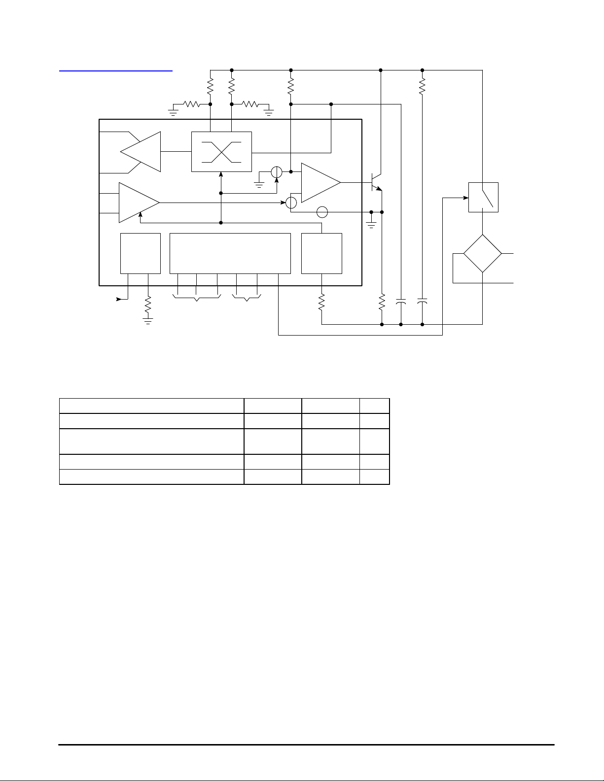
Representative Block Diagram
This device contains 610 active transistors + 242 gates.
R
x
T
x
Supply Serial Bus Interface AGC
Line
Driver
Serial Bus
Inputs
Logic
Outputs
R
x1
R
x2
T
x1
T
x2
R
x
Outputs
T
x
Inputs
HYS HYL LAI SRF
LAO
Gnd
VCCI
ref
Clk Data BEN Out1 Out2 HKSW AGC
Hook
Switch
A (Tip)
B (Ring)
I
BG
V
BG
+
–
MC34016
+5.0 V
MAXIMUM RATINGS
Rating Symbol Value Unit
Operation Supply Voltage V
CC
–0.5, 6.5 V
All Other Inputs V
in
–0.5,
VCC +0.5
V
Operating Ambient Temperature T
A
–20 to +70 °C
Junction Temperature T
J
+150 °C
NOTE: ESD data available upon request.
查询"MC34016"供应商
Freescale Semiconductor, Inc.
nc...
I
cale Semiconductor,
Frees
For More Information On This Product,
Go to: www.freescale.com
MC34016
3
MOTOROLA ANALOG IC DEVICE DATA
DC ELECTRICAL CHARACTERISTICS (All parameters are specified with Bit 0 of Register 1 set to 1, the rest of the
bits in both registers set to 0, TA = 25°C, VCC = 5.0 V, I
line
= 15 mA, f = 1.0 kHz, Test Circuit in Figure 9, unless otherwise noted.)
Parameter
Condition Min Typ Max Unit
VOLTAGE REGULATION
= 5.0 mA
Line Voltage V
line
I
line
= 5.0 mA
I
line
= 15 mA
3.7
4.2
4.0
4.5
4.3
4.8
V
line
= 15 mA
I
line
= 60 mA
CURRENT REGULATION (Bit 4, Reg.1 = 1; Bit 1, Reg. 2 = 1; R
AGC
= 47 kΩ)
Line Voltage V
line
I
line
= 15 mA 4.2 4.5 4.8 V
line
line
= 10 V
Line Current I
line
V
line
= 10 V
V
line
= 35 V
––3556––mA
Line Current I
line
in Protection Mode V
line
= 70 V – 28 – mA
DC BIASING
Operating Supply Voltage V
CC
– 3.0 – 5.5 V
CC
CC
= 3.0 V, all Bits to 0
Current Consumption from V
CC
VCC = 3.0 V, all Bits to 0
VCC = 5.0 V, all Bits to 0
––3.0
3.5
4.0
4.5
mA
Source Capabiltiy Pin LAO in Speech Mode V
LAO
= 0.7 V – – –2.0 mA
Source Capability Pin LAO in Dialing Mode
(Bit 5, Reg. 1 = 1)
V
LAO
= 0.7 V – – –5.0 mA
Internal Pull Down Resistor at Pin LAO – – 11 – kΩ
Bias Voltage at Pins HYL, HYS and LAI – – 1.3 – V
Bias Voltage at Pins Tx1 and T
x2
– – 1.5 – V
Bias Voltage at Pins Rx1 and R
x2
– – 1.3 – V
LOGIC INPUTS
Logic Low Level Pins Clk, Data, BEN – – – 0.6 V
Logic High Level Pins Clk, Data, BEN – 2.2 – – V
LOGIC OUTPUTS
Source Capability from Pins HKSW, Out1, Out2 Output Voltage at VCC – 1.3 V – – –1.0 mA
Sink Capability into Pins HKSW, Out1, Out2 Output Voltage at 0.5 V 5.0 – – mA
AC ELECTRICAL CHARACTERISTICS (All parameters are specified with Bit 0 of Register 1 set to 1, the rest of the
bits in both registers set to 0, TA = 25°C, VCC = 5.0 V, I
line
= 15 mA, f = 1.0 kHz, Test Circuit in Figure 9, unless otherwise noted.)
Parameter
Condition Min Typ Max Unit
TRANSMIT CHANNEL
Transmit Gain from VTx to V
line
MC34016P
MC34016DW
VTx = 0.1 Vrms
–1.0
–1.25
0.25
–0.20
1.5
0.85
dB
Gain Variation with Line Current Referred to
I
line
= 15 mA with the AGC Function Switched “Off”
I
line
= 70 mA,
Bit 0, Reg. 2 = 1
–0.7 – 0.7 dB
Gain Increase in 6.0 dB Mode Bit 4, Reg. 2 = 1 5.3 6.0 6.7 dB
Gain Reduction in Mute Condition Bit 2, Reg. 2 = 1 65 – – dB
Input Impedance at Tx1 or T
x2
– – 30 – kΩ
Maximum Input Swing for VT
x
THD ≤ 2% – 4.0 – Vpp
THD at the Line (V
line
) VTx = 3.0 dBm – 1.0 2.0 %
Psophometrically Weighted Noise Level at the Line
(V
line)
200 Ω Between Tx1 and T
x2
– –79 – dBmp
RECEIVE CHANNEL
Receive Gain from V
line
to VR
x
V
line
= 0.1 Vrms –1.0 0 1.0 dB
Gain Variation with Line Current Referred to
I
line
= 15 mA with the AGC Function Switched “Off”
I
line
= 70 mA,
Bit 0, Reg. 2 = 1
–0.7 – 0.7 dB
Freescale Semiconductor, Inc.
查询"MC34016"供应商
Line Voltage V
I
3.7 4.0 4.3 V
6.6 6.85 7.1
Line Current I
Current Consumption from V
nc...
I
cale Semiconductor,
Frees
For More Information On This Product,
Go to: www.freescale.com
V
V
–
–
35
3.0
–
4.0
mA
mA
MC34016
4
MOTOROLA ANALOG IC DEVICE DATA
AC ELECTRICAL CHARACTERISTICS (continued)
(All parameters are specified with Bit 0 of Register 1 set to 1, the rest of the
bits in both registers set to 0, TA = 25°C, VCC = 5.0 V, I
line
= 15 mA, f = 1.0 kHz, Test Circuit in Figure 9, unless otherwise noted.)
Parameter UnitMaxTypMinCondition
RECEIVE CHANNEL
Gain Increase in 6.0 dB Mode Bit 5, Reg. 2 = 1 5.3 6.0 6.7 dB
Gain Reduction in Mute Condition Bit 3, Reg. 2 = 1 70 – – dB
Input Impedance at HYL or HYS – – 30 – kΩ
Output Impedance at Rx1 or R
x2
– – 150 – Ω
Maximum Input Swing at HYL or HYS for THD ≤ 2% – 800 – mVpp
Maximum Output Swing VR
x
for THD ≤ 10% – 3.5 – Vpp
Total Harmonic Distortion at VR
x
V
line
= 3.0 dBm – 1.0 2.0 %
Psophometrically Weighted Noise Level at VR
x
200 Ω Between Tx1 and T
x2
– 80 – µVrms
AUTOMATIC GAIN CONTROL
Gain Reduction in Transmit and Receive Channel with
Respect to I
line
= 15 mA
I
line
= 70 mA 5.0 6.0 7.0 dB
Highest Line Current for Maximum Gain – – 20 – mA
Lowest Line Current for Minimum Gain – – 60 – mA
Gain Reduction in Transmit and Receive Channel with
Respect to I
line
= 35 mA
I
line
= 85 mA,
Bit 1, Reg. 2 = 1
5.0 6.0 7.0 dB
Highest Line Current for Maximum Gain Bit 1, Reg. 2 = 1 – 40 – mA
Lowest Line Current for Minimum Gain Bit 1, Reg. 2 = 1 – 80 – mA
BALANCE RETURN LOSS
Balance Return Loss with Respect to 600Ω f = 1.0 kHz 20 – – dB
SIDETONE
Voltage Gain from VTx to VR
x
I
line
= 15 mA,
Bit 0, Reg. 2 = 1
– – –20 dB
SERIAL BUS
Clock Frequency – – – 550 kHz
BEN Rising Edge Setup Time Before First Clk Rising
Edge
See t1 in Timing Diagram 500 – – ns
Data Setup Time Before Clk Rising Edge See t2 in Timing Diagram 500 – – ns
Data Hold Time After Clk Rising Edge See t3 in Timing Diagram 500 – – ns
BEN Falling Edge Delay Time After Last Clk Rising
Edge
See t4 in Timing Diagram 1.5 – – µs
BEN Rising Edge Delay Time After Last BEN Falling
Edge
See t5 in Timing Diagram 6.0 – – µs
Power Supply Reset Voltage V
CC
– – 2.5 – V
Freescale Semiconductor, Inc.
nc...
I
cale Semiconductor,
Frees
查询"MC34016"供应商
For More Information On This Product,
Go to: www.freescale.com
MC34016
5
MOTOROLA ANALOG IC DEVICE DATA
PIN FUNCTION DESCRIPTION
Pin Symbol Description
1 Clk Serial bus clock input
2 Data Serial bus data input
3 Out2 Logic output 2
4 Stab Line driver compensation
5 Gnd Ground
6 HKSW Logic output for the hook switch
7 Out1 Logic output 1
8 V
CC
Supply input (+5.0 V)
9 I
ref
Reference current adjustment
10 HYL Hybrid input for long lines
11 HYS Hybrid input for short lines
12 R
x2
Receive output 2
13 R
x1
Receive output 1
14 T
x1
Transmit input 1
15 T
x2
Transmit input 2
16 AGC Automatic gain control input
17 SRF Sidetone reference input
18 LAI Line amplifier input
19 LAO Line amplifier output
20 BEN Serial bus enable input
Freescale Semiconductor, Inc.
查询"MC34016"供应商
nc...
I
cale Semiconductor,
Frees
For More Information On This Product,
Go to: www.freescale.com

MC34016
6
MOTOROLA ANALOG IC DEVICE DATA
DESCRIPTION OF THE CIRCUIT
Throughout this part, please refer to the typical application
of Figure 10. The data given in this chapter refers to typical
data of the characteristics.
DC OPERATION
For dc, the MC34016 incorporates four different masks
which can be selected via the serial bus interface:
Bit 4, Reg. 1
‘DC Mask’
Bit 5, Reg. 1
‘DC Mode’
Bit 1, Reg. 2
‘AGC Ratio’
DC Mask
Selected
0
0
X
Voltage Regulation Mask
X
1
X
Pulse Dial Mask
1
0
0
Current Regulation Mask with
AGC Ratio 1:2
1
0
1
Current Regulation Mask with
AGC Ratio 3:5
X = don’t care
Voltage Regulation Mask
The voltage regulation mask is the default setting of the
MC34016 after power–up. In this mode, the circuit behaves
as a zener with a series resistor. The line voltage can be
expressed as:
V
line
= VBG + (IBG x R
DC1
) + (I
line
x RS)
with: VBG=1.3 V
IBG= 5.2 µA
R
DC1
= DC setting resistor of 470 kΩ in the typical
application
I
line
= Line current
RS= Slope resistor of 50 Ω in the typical
application
thus: V
line
= 3.75 + (50 x I
line
)
By choosing different values of R
DC1
, the zener voltage
can be adjusted to fit country specific requirements. In
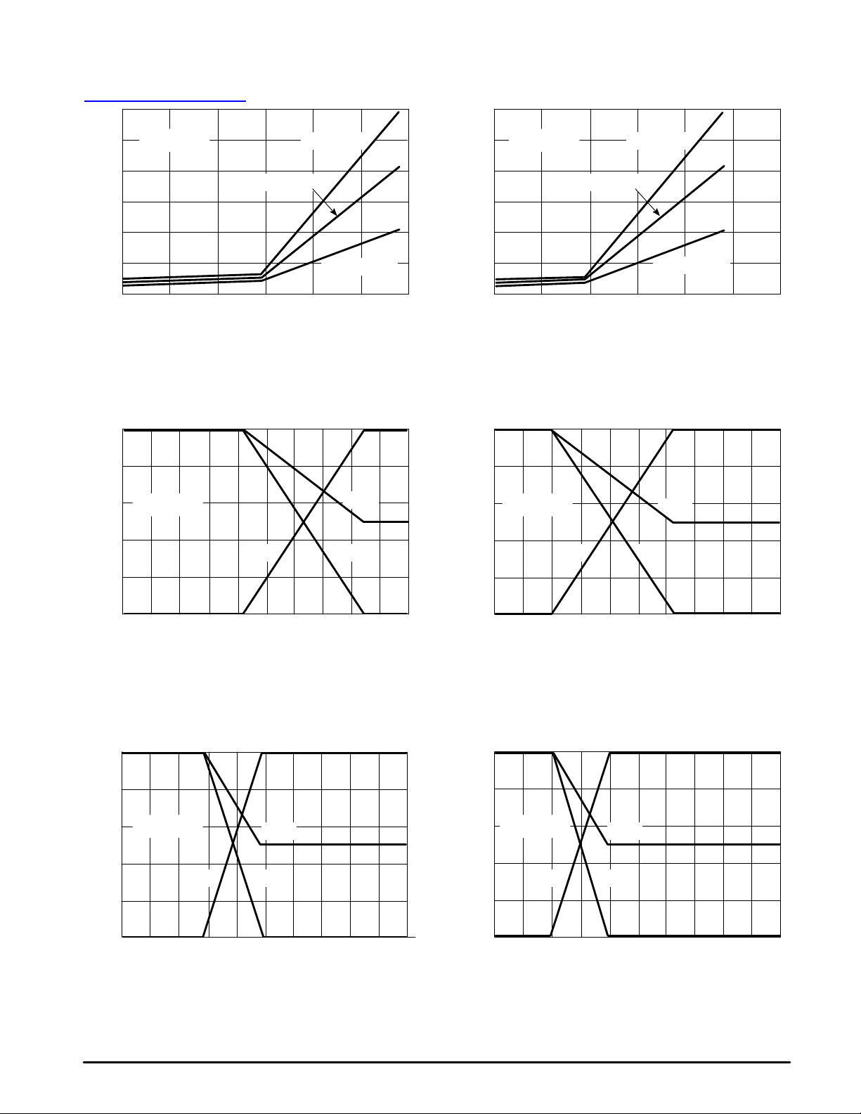
Figure 1, a curve shows V
line
versus I
line
for different R
DC1
values.
Pulse Dial Mask
In this mask, the circuit is forced into a very low voltage
drop mode meant for pulse dialing (e.g. make period during
pulse dialing). Pin LAO of the MC34016 sources a current of
5.0 mA in this mode, saturating output transistor Q1. The line
voltage V
line
is now determined by the saturation voltage of
Q1 and the dc slope resistor RS:
V
line
= V
CE(sat)Q1
+ (RS x I
line
) ≅ 0.1 + (50 x I
line
)
Figure 2 shows V
line
versus I
line
.
Current Regulation Masks
These masks are equal to the voltage regulation mask up
to a knee current. Above this current, the dc slope changes to
a higher value fulfilling requirements such as those in France.
V
line
= 3.75 + (RS x I
line
) for I
AGC
< I
knee
V
line
= [IBG + (2.5 x (I
AGC
– I
knee
))] x R
DC1
+
[VBG + (RS x I
line
)] for I
AGC
> I
knee
with : I
AGC
+
I
line
x
R
S
R
AGC
I
knee
= 21 µA for AGC ratio 1:2
I
knee
= 31 µA for AGC ratio 3:5
With RS = 50 Ω and R
AGC
= 47 kΩ, and the AGC ratio set
to 3:5, I
AGC
will equal I
knee
at a line current of 29 mA. With the
AGC ratio set to 1:2, the knee occurs at 20 mA. Above these
line currents, it can be derived that the dc slope of the circuit
changes to:
R
Slope
+
2.5 x
RSx R
DC1
R
AGC
)
R
S
With the component values mentioned, a slope of 1300 Ω
will occur. Figures 3 and 4 shows V
line
versus I
line
in the two
current regulation masks for different values of R
DC1
.
When I
AGC
reaches 62 µA for AGC ratio 3:5 or 52 µA in
case of AGC ratio 1:2, the MC34016 will enter protection
mode after about 800 ms. In practice this mode occurs only
under overload conditions. In protection mode, the MC34016
decreases the power dissipation in Q1 by drastically
increasing the dc slope starting from I
knee
. This results in a
reduced line current which remains practically constant over
line voltage. With the equation for Iagc it can be derived that:
ÁÁÁÁ
ÁÁÁÁ
ÁÁÁÁ
ÁÁÁÁ
AGC ratio
Line Current to Enter
Protection Mode
Line Current in
Protection Mode
ÁÁÁÁ
ÁÁÁÁ
ÁÁÁÁ
3:5
58 mA
29 mA
ÁÁÁÁ
ÁÁÁÁ
ÁÁÁÁ
1:2
49 mA
20 mA
Once the MC34016 enters protection mode, it remains
there until the output HKSW is toggled via Bit 0 of Register 1
(on–hook, off–hook).
Supply Voltage V
CC
The MC34016 operates from an external supply within a
voltage range of 3.0 to 5.5 V. The current consumption with
all bits set to 0, equals 3.0 mA at 3.0 V and 3.5 mA at 5.5 V.
AC SET IMPEDANCE
The MC34016 offers two possibilities for the adjustment of
the ac set impedance. Either a passive or an active set
impedance can be obtained.
Passive Set Impedance
In this application, the set impedance is formed by the ac
impedance of the circuit itself in parallel with resistor R
SET
and capacitor C
SET
. An equivalent network equals:
R
DC1
C
M
R
DC1
x CM x R
S
R
S
C
SET
R
SET
nc...
I
cale Semiconductor,
Frees
Freescale Semiconductor, Inc.
查询"MC34016"供应商
For More Information On This Product,
Go to: www.freescale.com

MC34016
7
MOTOROLA ANALOG IC DEVICE DATA
With the component values of the typical application, the
inductor has a value of about 2.4 H and R
DC1
equals 470 kΩ.
In the audio range of 300–3400 Hz, these components form
a fairly large parallel impedance to R
SET
and C
SET
.
Therefore, the set impedance is mainly determined by the
passive network R
SET
and C
SET
. In the typical application,
R
SET
is 600 Ω, but it can easily be replaced by a complex
network to obtain a complex set impedance.
Active Set Impedance
An active set impedance can b e obtained by placing a
resistor between pin LAI and SRF (R
SRF
) as shown in
Figure 11. By doing so, the MC34016 itself generates the ac
set impedance and R
SET
and C
SET
can be omitted. An
equivalent network now equals:
R
DC1
C
M
R
DC1
x CM x R
S
R
S
((R
DC1
+ R
SRF
) x RS/R
SRF
) – R
S
R
SRF
Ignoring the effect o f the inductor and the parallel path
R
DC1
+ R
SRF
again for audio frequencies, the set
impedance is now determined by:
Z
SET
+
R
S
R
SRF
x (R
DC1
)
R
SRF
)
With RS = 50 Ω and R
DC1
= 470 kΩ, R
SRF
should be 43 kΩ
to obtain a 600 Ω set impedance. To obtain a complex set
impedance, R
DC1
can be made complex. In such case, the
dc mask can be adjusted with the dc value of R
DC1
and the
set impedance can be adjusted with the ac value of R
DC1
. An
application with an active set impedance is interesting,
particularly in countries like France, where with the dc current
regulation mask, rather high line voltages can be reached.
With a passive set impedance, this would result in a high cost
for capacitor C
SET
.
TRANSMIT CHANNEL
Inputs
The inputs Tx1 and Tx2 are designed to handle large signal
levels of up to +3.0 dBm. The input impedance for both T
x1
and Tx2 equals 30 kΩ. The inputs are designed for
symmetrical as well as asymmetrical use. In asymmetrical
drive, one input can be tied to Gnd via an external capacitor.
Gain
The gain from inputs Tx1 and Tx2 to the line is dependent
on the set impedance, the line load impedance and dc slope
resistor RS in the following way:
ATX+
1
6 x R
S
x
Z
SET
x Z
line
Z
SET
)
Z
line
With Z
SET
= 600 Ω, Z
line
= 600 Ω and RS = 50 Ω the gain
equals 0 dB. By setting Bit 4 of Register 2 to 1, the gain is
raised by 6.0 dB.
Outputs
In order to transmit signals to the line, the output stage of
the MC34016 (line driver) modulates the zener previously
described. To guarantee stability of the output stage
capacitor C
STB
of 100 pF is required
SIDETONE
The MC34016 is equipped with a double Wheatstone
bridge architecture to optimize sidetone. One sidetone
network is used for short lines and one for long lines.
Switchover between both networks is dependent on line
current and is described in the automatic gain control section.
Different sidetone equations apply depending on whether a
passive or an active set impedance is set.
Sidetone Cancellation with Passive Set Impedance
In a passive set impedance application, the set impedance
is a part of the equations for optimum sidetone. For short
lines optimum cancellation occurs if:
Z
HS1
+
R
HS2
R
S
x
Z
SET
x Z
lineshort
Z
SET
)
Z
lineshort
with: Z
lineshort
= impedance of a short telephone line
and for long lines:
Z
HL1
+
R
HL2
R
S
x
Z
SET
x Z
linelong
Z
SET
)
Z
linelong
with: Z
linelong
= impedance of a long telephone line
Sidetone Cancellation with Active Set Impedance
In the active set impedance application, the set impedance
does not appear in the equations for optimum sidetone
cancellation as it does in the passive application. For short
lines, optimum cancellation occurs if:
Z
HS1
+
R
HS2
R
S
x Z
lineshort
and for long lines:
Z
HL1
+
R
HL2
R
S
x Z
linelong
RECEIVE CHANNEL
Inputs
The inputs HYS and HYL have an input resistance of 30 kΩ
and can handle signals up to 800 mVpp. This corresponds to a
signal at the telephone line of about 8.0 dBm in the typical
application. The switchover from HYS to HYL is dependent on
line current and described in the automatic gain control
section.
Gain
The overall gain from the line to the outputs Rx1 and R
x2
for short lines and passive impedance equals:
ARX+
7.6 x
R14′
R14′)Z
HYS
For active impedance it follows:
ARX+
7.6 x
R14′
R14′)Z
HYS
xǒ1
)
R1 x Z
HYS
R14 x Z
SET
Ǔ
In these relations, R14′ is the resistor R14 in parallel with
the input impedance at HYS of 30 kΩ. The gain for long
lines can be derived by replacing Z
HYS
and R14 by Z
HYL
Freescale Semiconductor, Inc.
nc...
I
cale Semiconductor,
Frees
查询"MC34016"供应商
For More Information On This Product,
Go to: www.freescale.com

MC34016
8
MOTOROLA ANALOG IC DEVICE DATA
and R17. With R14 = 3.0 kΩ and Z
HYS
= 18 kΩ the receive
gain equals 0 dB for the passive impedance application.
Outputs
The outputs Rx1 and Rx2 of the receive channel have an
output impedance of 150 Ω and are designed to drive a 10 kΩ
resistive load or a 47 nF capacitive load with a 3.5 Vpp swing.
AUTOMATIC GAIN CONTROL
The automatic gain control function (AGC) controls the
transmit and receive gains and the switchover for the
sidetone networks for short and long lines according to the
line current (which represents line length). The effect of AGC
on the transmit and receive amplifiers is 6.0 dB at default and
it can be disabled via the serial bus. The switchover for the
sidetone networks tracks the AGC curves for the transmit
and receive amplifier gain. This feature can also be disabled
via the serial bus:
Bit 6, Reg. 2
‘PABX Mode’
Bit 0, Reg. 2
‘AGC Range’
Description
0
0
AGC Gain Range of 6.0 dB,
Sidetone Switchover Enabled
0
1
No AGC Gain Range, Sidetone
Switchover Enabled
1
0
AGC Range of 6.0 dB, only
HYS Input Active, HYL Muted
1
1
No AGC Gain Range, only
HYS Input Active, HYL Muted
The ratio between start and stop current for the AGC
curves is programmable for both voltage and current
regulation mode:
Bit 4,
Reg. 1
‘DC
Mask’
Bit 1,
Reg. 2
‘AGC
Ratio’
AGC Ratio
Selected
I
AGCstart
(µA)
I
AGCstop
(µA)
0
0
Voltage Regulation, AGC
Ratio 1:3
10
31
0
1
Voltage Regulation, AGC
Ratio 1:2
21
42
1
0
Current Regulation, AGC
Ratio 1:2
21
42
1
1
Current Regulation, AGC
Ratio 3:5
31
52
The relation between line current and I
start
and I
stop
is
given by:
I
linestart
+
R
AGC
R
S
x I
AGCstart
I
linestop
+
R
AGC
R
S
x I
AGCstop
Figures 5, 6, 7 and 8 show the AGC curves for both
voltage regulation and current regulation. In current
regulation, the start point for the AGC curves is coupled to the
knee point of the dc characteristic, or: I
knee
= I
AGCstart
.
LOGIC OUTPUT DRIVERS
The MC34016 is equipped with three logic outputs meant
to interface to the front end of a telephone. The outputs can
be controlled via the serial bus interface. As shown in the
characteristics, the logic outputs are capable of sourcing at
least 1.0 mA and sinking at least 5.0 mA.
Output HKSW
Output HKSW is dedicated to drive the hookswitch. With
HKSW low, the line is opened via Q2 and Q3 and
automatically switches off the line driver transistor Q1. This
feature guarantees fast dc settling after line breaks occurring
during pulse dialing.
Outputs Out1 and Out2
Outputs Out1 and Out2 may be used for any logic function,
such as control of an earth switch and/or a shunt wire.
SERIAL BUS INTERFACE
The serial interface of the MC34016 enables a simple
three wire connection to a micro controller.
Timing
Times t1, t2, t3, t4 and t5 are specified in the electrical
characteristics.
With BEN high, data can be clocked into the serial port by
using Data and Clk lines. On the rising edge of the Clk, the
data enters the MC34016. The last 8–bits of data entered are
shifted into the registers when BEN is forced low. With BEN
low, the serial port of the MC34016 is disabled. BEN must be
kept low until the next register update is needed. Data should
be written by entering the most significant bit first (Bit 7) and
the least significant bit (Bit 0) last.
With BEN low, the Data and Clk lines may be used to
control other devices in the application.
Freescale Semiconductor, Inc.
nc...
I
cale Semiconductor,
Frees
查询"MC34016"供应商
For More Information On This Product,
Go to: www.freescale.com

MC34016
9
MOTOROLA ANALOG IC DEVICE DATA
Timing Diagram
Bit 7 Bit 6 Bit 5 Bit 4 Bit 3 Bit 2 Bit 1 Bit 0
t1 t2 t3 t4 t5
Clk
Data
BEN
Registers
The MC34016 is equipped with two 8–bit registers which
are selected by the value of the most significant bit (Bit 7). If
the supply voltage of the MC34016 drops below 2.5 V, all
registers are set to 0. This RESET function enables a smooth
power–up of the device. The registers are as follows:
Register 1 (Bit 7 = 0)
Bit
Function
Operation
Default
0
Output
HKSW
0: HKSW is Low
1: HKSW is High
0
1
Output
Out1
0: Out1 is Low
1: Out1 is High
0
2
Output
Out2
0: Out2 is Low
1: Out2 is High
0
3
Not Used
–
–
4
DC Mask
0: Voltage Regulation Mask
1: Current Regulation Mask for
France
0
5
DC Mode
0: Speech Mode/Normal Operation
1: Dialing Mode for Low Voltage
Drop
0
6
Test Mode
Only Used During Manufacturing
0
Register 2 (Bit 7 = 1)
ÁÁ
ÁÁ
ÁÁ
Bit
Function
Operation
Default
ÁÁ
ÁÁ
ÁÁ
0
AGC
Range
0: AGC Range 6.0 dB
1: AGC Range 0 dB (Switched “Off”)
0
ÁÁ
ÁÁ
ÁÁ
ÁÁ
ÁÁ
ÁÁ
1
AGC
Ratio
Voltage
Regulation:
(Bit 4,
Reg. 1 = 0)
0: Ratio 1:3
1: Ratio 1:2
Current
Regulation:
(Bit 4,
Reg. 1 = 1)
0: Ratio 1:2
1: Ratio 3:5
0
ÁÁ
ÁÁ
ÁÁ
ÁÁ
2
Transmit
Mute
0: Transmit Channel Active
1: Transmit Channel Muted
0
ÁÁ
ÁÁ
ÁÁ
ÁÁ
3
Receive
Mute
0: Receive Channel Active
1: Receive Channel Muted
0
ÁÁ
ÁÁ
ÁÁ
4
Transmit
Gain
0: Transmit Channel Gain = 0 dB
1: Transmit Channel Gain = 6.0 dB
0
ÁÁ
ÁÁ
ÁÁ
ÁÁ
5
Receive
Gain
0: Receive Channel Gain = 0 dB
1: Receive Channel Gain = 6.0 dB
0
ÁÁ
ÁÁ
ÁÁ
ÁÁ
6
PABX
Mode
0: Normal Mode
1: PABX Mode (only Input HYS
Selected)
0
0
6.0
0
10
I
line
, LINE CURRENT (mA)
Figure 1. Line Voltage versus Line Current
(Voltage Regulation Mask)
I
line
, LINE CURRENT (mA)
Figure 2. Line Voltage versus Line Current
(Pulse Dial Mask)
R
DC1
= 680 k
, LINE VOLTAGE (V)
R
DC1
= 470 k
R
DC1
= 220 k
0
2.0
4.0
6.0
8.0
5.0
4.0
3.0
2.0
1.0
0
10 20 30 40 50 60 70 80 90 100 10 20 30 40 50
60
70 80 90 100
V
line
Freescale Semiconductor, Inc.
查询"MC34016"供应商
nc...
I
cale Semiconductor,
Frees
For More Information On This Product,
Go to: www.freescale.com
, LINE VOLTAGE (V)V
line
MC34016
10
MOTOROLA ANALOG IC DEVICE DATA
0
1.0
0
60
0
1.0
0
60
AGC WEIGHTING FACTOR
I
line
, LINE CURRENT (mA)
AGC WEIGHTING FACTOR
I
line
, LINE CURRENT (mA)
V
line
, LINE VOLTAGE (V)
I
line
, LINE CURRENT (mA)
AGC WEIGHTING FACTOR
I
line
, LINE CURRENT (mA)
AGC WEIGHTING FACTOR
I
line
, LINE CURRENT (mA)
V
line
, LINE VOLTAGE (V)
Figure 3. Line Voltage versus Line Current
(Current Regulation Mask)
I
line
, LINE CURRENT (mA)
Figure 4. Line Voltage versus Line Current
(Current Regulation Mask)
R
AGC
= 47 k
AGC Ratio 3:5
Figure 5. AGC Weighting Factor versus I
line
(Voltage Regulation Mask)
Figure 6. AGC Weighting Factor versus I
line
(Voltage Retulation Mask)
Figure 7. AGC Weighting Factor versus I
line
(Current Regulation Mask)
Figure 8. AGC Weighting Factor versus I
line
(Currrent Regulation Mask)
R
DC1
= 680 k
R
DC1
= 470 k
R
DC1
= 220 k
R
AGC
= 47 k
AGC Ratio 1:2
R
AGC
= 100 k
AGC Ratio 1:2
R
AGC
= 100 k
AGC Ratio 1:3
R
DC1
= 680 k
R
DC1
= 470 k
R
DC1
= 220 k
Gain
HYLHYS HYLHYS
50
40
30
20
10
0
50
40
30
20
10
0
0.8
0.6
0.4
0.2
0
0.8
0.6
0.4
0.2
0
10 20 30 40 50 60 10 20 30 40 50 60
10 20 30 40 50 60 70 80 90 100 10 20 30 40 50 60 70 80 90 100
Gain
0
1.0
0.8
0.6
0.4
0.2
0
10 20 30 40 50 60 70 80 90 100
R
AGC
= 47 k
AGC Ratio 1:2
Gain
HYLHYS
0
1.0
0.8
0.6
0.4
0.2
0
10 20 30 40 50 60 70 80 90 100
R
AGC
= 47 k
AGC Ratio 3:5
Gain
HYLHYS
查询"MC34016"供应商
Freescale Semiconductor, Inc.
nc...
I
cale Semiconductor,
Frees
For More Information On This Product,
Go to: www.freescale.com

MC34016
11
MOTOROLA ANALOG IC DEVICE DATA
Figure 9. Test Diagram
I
line
15 mA
Line
Driver
Supply Serial Bus Interface AGC
R
x
T
x
R
x1
R
x2
T
x1
T
x2
LAO
Gnd
Stab
HYS HYL LAI SRF
VCCI
ref
Clk Data BEN Out1 Out2 HKSW AGC
V
BG
I
BG
R
HL1
18 k
R
DC1
470 k
C
Stab
100 p
R
SET
600
R
HS1
18 k
C
HL1
0.047
C
HS1
0.047
R
HS2
R
HL2
3.0 k 3.0 k
CRx1 0.1
CRx2 0.1
RR
x
10 k
CTx1 0.047
CTx2 0.047
Q1
MJE340
R
AGC
100 k
R
S
50
C
M
0.1
C
SET
4.7
µ
C
line
47
µ
R
line
600
VAC V
line
V
A A A
+ + +
+ +
R
ref
59 k
V
CC
5.0 V
From MPU
MC34016
VR
x
V
+
VT
x
Freescale Semiconductor, Inc.
查询"MC34016"供应商
nc...
I
cale Semiconductor,
Frees
For More Information On This Product,
Go to: www.freescale.com

MC34016
12
MOTOROLA ANALOG IC DEVICE DATA
Figure 10. Typical Application with Passive Impedance and Voltage Regulation
Line
Driver
Supply Serial Bus Interface AGC
R
x
T
x
R
x1
R
x2
T
x1
T
x2
LAO
Gnd
Stab
HYS HYL LAI SRF
VCCI
ref
Clk Data BEN Out1 Out2 HKSW AGC
V
BG
I
BG
R
HL1
18 k
R
DC1
470 k
C
Stab
100 p
R
SET
600
R
HS1
18 k
C
HL1
0.047
C
HS1
0.047
R
HS2
R
HL2
3.0 k 3.0 k
CRx1 0.047
CRx2 0.047
CTx1 0.047
CTx2 0.047
Q1
R
AGC
100 k
R
S
50
C
M
0.1
C
SET
4.7
µ
R
ref
59 k
Q3
MPSA42
Q2
MJE350
Receive
Outputs
Transmit
Inputs
Supply
From
MPU
V
line
D2D1
D4D3
B, Ring
A, Tip
Optional
Shunt
Earth
R
INT
560
1N4004
MC34016
+
NOTE: Sidetone Networks not adapted to country specific telephone lines.
查询"MC34016"供应商
Freescale Semiconductor, Inc.
nc...
I
cale Semiconductor,
Frees
For More Information On This Product,
Go to: www.freescale.com

MC34016
13
MOTOROLA ANALOG IC DEVICE DATA
Figure 11. Typical Application with Active Impedance and Current Regulation
Line
Driver
Supply Serial Bus Interface AGC
R
x
T
x
R
x1
R
x2
T
x1
T
x2
LAO
Gnd
Stab
HYS HYL LAI SRF
VCCI
ref
Clk Data BEN Out1 Out2 HKSW AGC
V
BG
I
BG
R
HL1
36 k
R
DC1
470 k
C
Stab
100 p
R
HS1
36 k
C
HL1
0.047
C
HS1
0.047
R
HS2
R
HL2
3.0 k 3.0 k
CRx1 0.047
CRx2 0.047
CTx1 0.047
CTx2 0.047
Q1
MJE340
R
AGC
100 k
R
S
50
C
M
0.1
R
ref
59 k
Q3
MPSA42
Q2
MJE350
Receive
Outputs
Transmit
Inputs
Supply
From
MPU
V
line
D2D1
D4D3
B, Ring
A, Tip
Optional
Shunt
Earth
R
INT
1.8 k
1N4004
MC34016
+
R
SRF
43 k
NOTE: Sidetone Networks not adapted to country specific telephone lines.
Freescale Semiconductor, Inc.
查询"MC34016"供应商
nc...
I
cale Semiconductor,
Frees
For More Information On This Product,
Go to: www.freescale.com

MC34016
14
MOTOROLA ANALOG IC DEVICE DATA
P SUFFIX
PLASTIC PACKAGE
CASE 738–03
ISSUE E
DW SUFFIX
PLASTIC PACKAGE
CASE 751D–04
ISSUE E
OUTLINE DIMENSIONS
NOTES:
1. DIMENSIONING AND TOLERANCING PER
ANSI Y14.5M, 1982.
2. CONTROLLING DIMENSION: MILLIMETER.
3. DIMENSIONS A AND B DO NOT INCLUDE
MOLD PROTRUSION.
4. MAXIMUM MOLD PROTRUSION 0.150
(0.006) PER SIDE.
5. DIMENSION D DOES NOT INCLUDE
DAMBAR PROTRUSION. ALLOWABLE
DAMBAR PROTRUSION SHALL BE 0.13
(0.005) TOTAL IN EXCESS OF D DIMENSION
AT MAXIMUM MATERIAL CONDITION.
–A–
–B–
20
1
11
10
S
A
M
0.010 (0.25) B
S
T
D20X
M
B
M
0.010 (0.25)
P10X
J
F
G
18X
K
C
–T–
SEATING
PLANE
M
R
X 45
_
DIM MIN MAX MIN MAX
INCHESMILLIMETERS
A 12.65 12.95 0.499 0.510
B 7.40 7.60 0.292 0.299
C 2.35 2.65 0.093 0.104
D 0.35 0.49 0.014 0.019
F 0.50 0.90 0.020 0.035
G 1.27 BSC 0.050 BSC
J 0.25 0.32 0.010 0.012
K 0.10 0.25 0.004 0.009
M 0 7 0 7
P 10.05 10.55 0.395 0.415
R 0.25 0.75 0.010 0.029
_ _
_ _
1.070
0.260
0.180
0.022
0.070
0.015
0.140
15
°
0.040
1.010
0.240
0.150
0.015
0.050
0.008
0.110
0
°
0.020
25.66
6.10
3.81
0.39
1.27
0.21
2.80
0
°
0.51
27.17
6.60
4.57
0.55
1.77
0.38
3.55
15
°
1.01
0.050 BSC
0.100 BSC
0.300 BSC
1.27 BSC
2.54 BSC
7.62 BSC
MIN MINMAX MAX
INCHES MILLIMETERS
DIM
A
B
C
D
E
F
G
J
K
L
M
N
NOTES:
1. DIMENSIONING AND TOLERANCING PER ANSI
Y14.5M, 1982.
2. CONTROLLING DIMENSION: INCH.
3. DIMENSION L TO CENTER OF LEAD WHEN
FORMED PARALLEL.
4. DIMENSION B DOES NOT INCLUDE MOLD
FLASH.
-A-
C
K
N
E
G F
D
20 PL
J 20 PL
L
M
-T-
SEATING
PLANE
1 10
1120
0.25 (0.010) T A
M M
0.25 (0.010) T B
M M
B
Freescale Semiconductor, Inc.
nc...
I
cale Semiconductor,
Frees
查询"MC34016"供应商
For More Information On This Product,
Go to: www.freescale.com

MC34016
15
MOTOROLA ANALOG IC DEVICE DATA
NOTES
Freescale Semiconductor, Inc.
查询"MC34016"供应商
nc...
I
cale Semiconductor,
Frees
For More Information On This Product,
Go to: www.freescale.com

MC34016
MC34016/D
*MC34016/D*
◊
..
.
nc
查询"MC34016"供应商
Freescale Semiconductor, Inc.
Freescale Semiconductor, I
For More Information On This Product,
Go to: www.freescale.com
 Loading...