

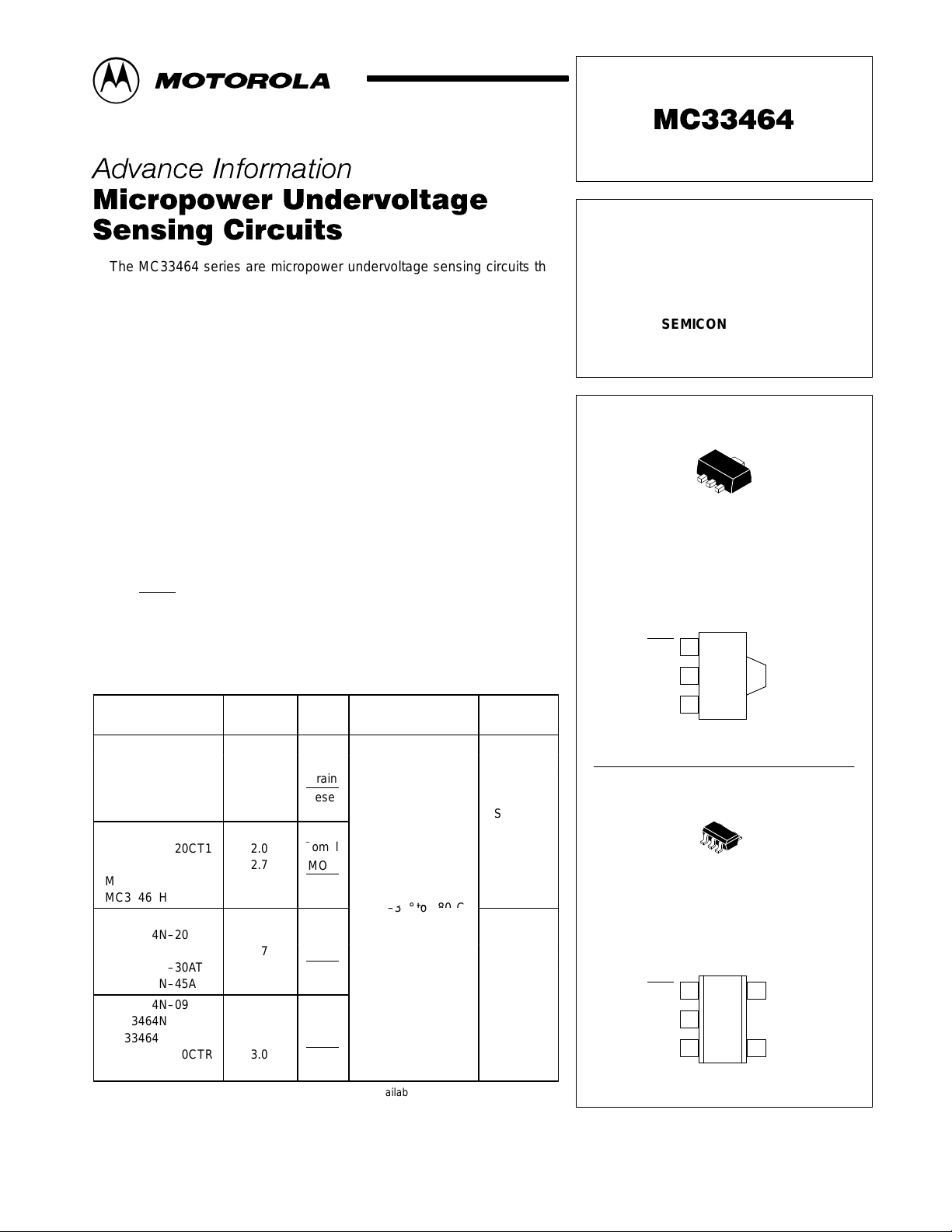
Motorola MC33464H-20CT1, MC33464H-27AT1, MC33464H-45CT1, MC33464H-30CT1, MC33464H-27CT1 Datasheet
...
Reset
SOT 89
Reset
T
30° t
80°C
Reset
SOT 23
Reset
Order this document by MC33464/D
The MC33464 series are micropower undervoltage sensing circuits that
are specifically designed for use with battery powered microprocessor based
systems, where extended battery life is required. A choice of several
threshold voltages from 0.9 V to 4.5 V are available. These devices feature a
very low quiescent bias current of 0.8 µA typical.
The MC33464 series features a highly accurate voltage reference, a
comparator with precise thresholds and built–in hysteresis to prevent erratic
reset operation, a choice of output configurations between open drain or
complementary MOS, and guaranteed operation below 1.0 V with extremely
low standby current. These devices are available in either SOT–89 3–pin or
SOT–23 5–pin surface mount packages.
Applications include direct monitoring of the MPU/logic power supply
used in portable, appliance, automotive and industrial equipment.
MC33464 Features:
• Extremely Low Standby Current of 0.8 µA at V
• Wide Input Voltage Range (0.7 V to 10 V)
• Monitors Power Supply Voltages from 1.1 V to 5.0 V
• High Accuracy Detector Threshold (±2.5%)
• Two Reset Output Types (Open Drain or Complementary Drive)
• Two Surface Mount Packages (SOT–89 or SOT–23 5–Pin)
ORDERING INFORMATION
Threshold
Device
MC33464H–09AT1 0.9
MC33464H–20AT1 2.0
MC33464H–27AT1 2.7
MC33464H–30AT1 3.0
MC33464H–45AT1 4.5
MC33464H–09CT1 0.9
MC33464H–20CT1 2.0
MC33464H–27CT1 2.7
MC33464H–30CT1 3.0
MC33464H–45CT1 4.5
MC33464N–09ATR 0.9
MC33464N–20ATR 2.0
MC33464N–27ATR 2.7
MC33464N–30ATR 3.0
MC33464N–45ATR 4.5
MC33464N–09CTR 0.9
MC33464N–20CTR 2.0
MC33464N–27CTR 2.7
MC33464N–30CTR 3.0
MC33464N–45CTR 4.5
Other voltages from 0.9 to 6.0 V , in 0.1 V increments, are available. Consult factory for
information.
Voltage
Open
Drain
Reset
Compl.
Reset
Open
Drain
Reset
Compl.
Reset
Temperature Range
Type
MOS
MOS
Operating
= –
A
= 1.5 V
in
°
o +
Package
(Qty/Reel)
SOT–89
(1000)
°
SOT–23
(3000)
MICROPOWER
UNDERVOLTAGE
SENSING CIRCUITS
SEMICONDUCTOR
TECHNICAL DATA
TAB
1
H SUFFIX
PLASTIC PACKAGE
CASE 1213
(SOT–89)
1
Reset
2
Input
Ground
3
(Top View)
5
1
N SUFFIX
PLASTIC PACKAGE
CASE 1212
(SOT–23)
15
Reset
2
Input
Ground
3
(Top View)
Tab
(Tab is connected
to Pin 2)
N/C
N/C
4
This document contains information on a new product. Specifications and information herein
are subject to change without notice.
MOTOROLA ANALOG IC DEVICE DATA
Motorola, Inc. 1996 Rev 0
1
MC33464
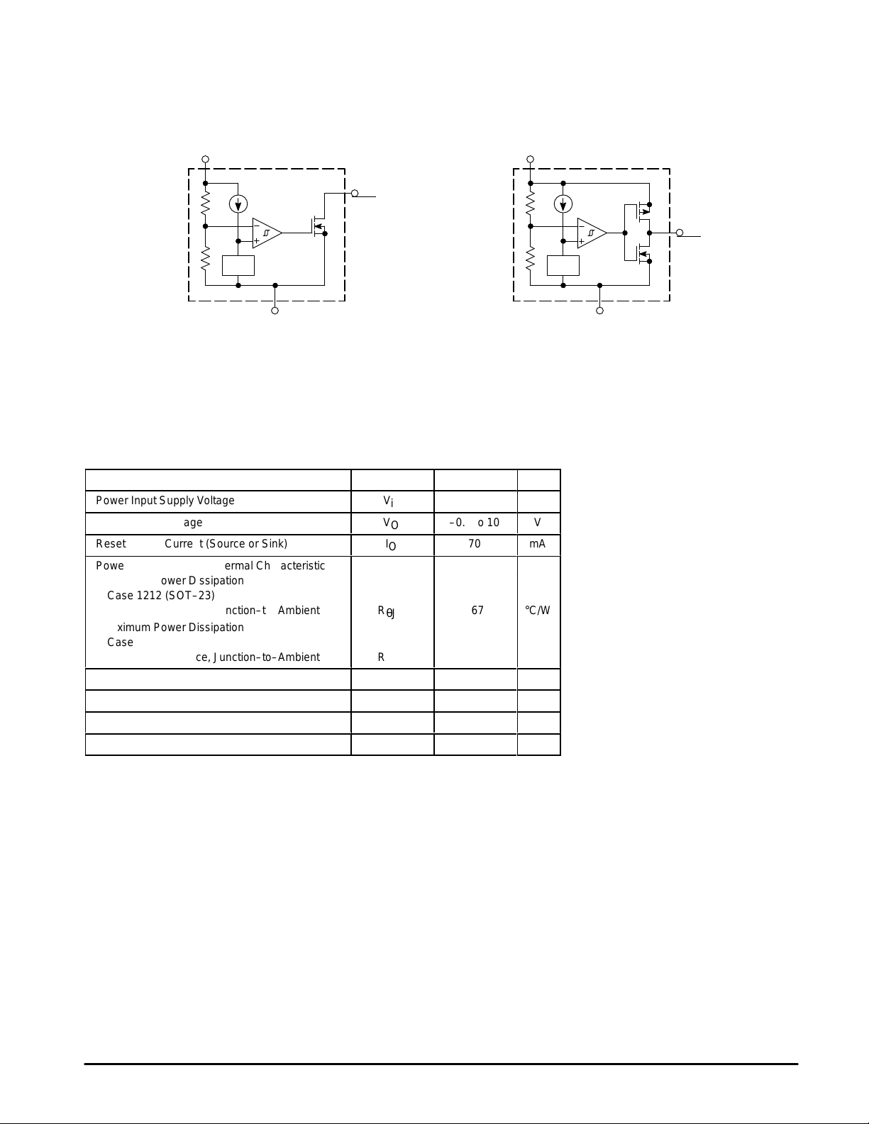
Representative Block Diagrams
MC33464X–YYATZ
Open Drain Configuration
2 Input
V
ref
3 Gnd
This device contains 25 active transistors.
MAXIMUM RATINGS (T
Power Input Supply Voltage
Reset Output Voltage
Reset Output Current (Source or Sink)
Power Dissipation and Thermal Characteristics
Maximum Power Dissipation
Case 1212 (SOT–23) N Suffix P
Thermal Resistance, Junction–to–Ambient R
Maximum Power Dissipation
Case 1213 (SOT–89) H suffix P
Thermal Resistance, Junction–to–Ambient R
Operating Junction Temperature
Operating Ambient Temperature
Storage Temperature Range
Lead Temperature (Soldering)
= 25°C, unless otherwise noted.)
C
Rating Symbol Value Unit
1
Reset
X Denotes Package Type
YY Denotes Threshold Voltage
TZ Denotes Taping Type
V
V
I
θJA
θJA
T
T
T
T
solder
in
O
O
D
D
J
A
stg
0 to 10
–0.3 to 10
–30 to +80
–40 to +125
260°C, 10 s
Complementary Drive Configuration
70
150 mW
667 °C/W
300 mW
333 °C/W
+125
MC33464X–YYCTZ
2 Input
V
ref
3 Gnd
V
V
mA
°C
°C
°C
–
1
Reset
2
MOTOROLA ANALOG IC DEVICE DATA
MC33464
ÁÁÁ
ÁÁÁ
ÁÁÁ
ÁÁÁ
ÁÁÁ
ÁÁÁ
ÁÁÁ
ÁÁÁ
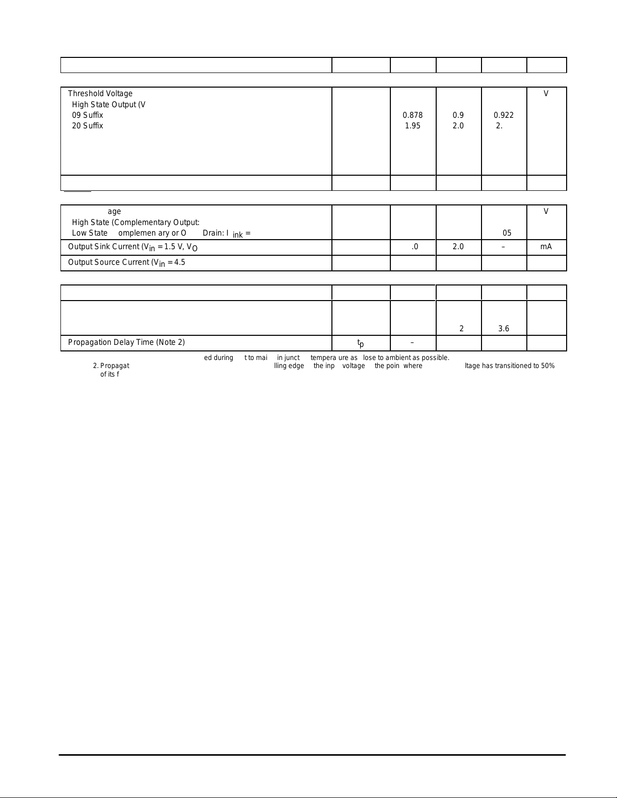
ELECTRICAL CHARACTERISTICS (For all values T
Characteristic
= 25°C (Note 1), unless otherwise noted.)
A
Symbol Min Typ Max Unit
COMPARATOR
Threshold Voltage
High State Output (Vin Decreasing) V
IH
09 Suffix 0.878 0.9 0.922
20 Suffix 1.95 2.0 2.05
27 Suffix 2.633 2.7 2.768
30 Suffix 2.925 3.0 3.075
45 Suffix 4.388 4.5 4.613
Threshold Hysteresis V
Threshold Voltage Temperature Coefficient
H
T
C
0.027 0.045 0.063 V
–
±100
RESET OUTPUT
Output Voltage
High State (Complementary Output: I
Low State (Complementary or Open Drain: I
Output Sink Current (Vin = 1.5 V, VOL = 0.5 V)
Output Source Current (Vin = 4.5 V, VOL = 2.4 V)
= 1.0 mA) V
source
= 1.0 mA) V
sink
I
I
OH
OH
OL
OL
Vin – 2.1 Vin – 1.0 V
– 0.025 0.05
1.0
1.0
2.0
2.0
TOTAL DEVICE
Operating Input Voltage Range
Quiescent Input Current
V
in
I
in
0.7 to 10
–
Vin = 2.9 V – 0.9 2.7
Vin = 5.6 V – 1.2 3.6
Propagation Delay Time (Note 2)
NOTES: 1. Low duty pulse techniques are used during test to maintain junction temperature as close to ambient as possible.
2.Propagation delay time is measured from the rising or falling edge of the input voltage to the point where the output voltage has transitioned to 50%
of its final value.
t
p
–
–
–
–
–
–
100
V
PPM/°C
V
in
mA
mA
V
µA
µs
MOTOROLA ANALOG IC DEVICE DATA
3
 Loading...