

Motorola MC33463H-33LT1, MC33463H-50KT1, MC33463H-50LT1, MC33463H-30LT1, MC33463H-33KT1 Datasheet
...
T
30° t
80°C
The MC33463 series are micropower step–up switching voltage
regulators, specifically designed for handheld and laptop applications, to
provide regulated output voltages using a minimum of external parts. A wide
choice of output voltages are available. These devices feature a very low
quiescent bias current of 4.0 µA typical.
The MC33463H–XXKT1 series features a highly accurate voltage
reference, an oscillator, a variable frequency modulation (VFM) controller, a
driver transistor (Lx), a comparator and feedback resistive divider.
The MC33463H–XXLT1 is identical to the MC33463H–XXKT1, except
that a drive pin (EXT) for an external transistor is provided.
Due to the low bias current specifications, these devices are ideally suited
for battery powered computer, consumer , and industrial equipment where an
extension of useful battery life is desirable.
MC33463 Series Features:
• Low Quiescent Bias Current of 4.0 µA
• High Output Voltage Accuracy of ±2.5%
Order this document by MC33463/D
VARIABLE FREQUENCY
MICROPOWER DC–to–DC
CONVERTER
SEMICONDUCTOR
TECHNICAL DATA
TAB
1
H SUFFIX
PLASTIC PACKAGE
CASE 1213
(SOT–89)
• Low Startup Voltage of 0.9 V at 1.0 mA
• Wide Output Voltage Range of 2.5 V to 7.5 V A vailable
• High Efficiency of 80% Typical
• Surface Mount Package
ORDERING INFORMATION
Output
Device
MC33463H–30KT1 3.0
MC33463H–33KT1 3.3
MC33463H–50KT1 5.0
MC33463H–30LT1 3.0
MC33463H–33LT1 3.3
MC33463H–50LT1 5.0
Other voltages from 2.5 V to 7.5 V , in 0.1 V increments are available. Consult factory for
information.
Voltage
Type
Int.
Switch
Ext.
Switch
Drive
Operating
Temperature Range
°
A
= –
o +
°
Package
(Tape/Reel)
SOT–89
SOT–89
(Tape)
(Tape)
PIN CONNECTIONS
MC33463H–XXKT1
1
Ground
2
Output
Lx
3
(Top View)
MC33463H–XXLT1
1
Ground
2
Output
EXT
3
(Top View)
Tab
(Tab is connected
to Pin 2)
Tab
(Tab is connected
to Pin 2)
This document contains information on a new product. Specifications and information herein
are subject to change without notice.
MOTOROLA ANALOG IC DEVICE DATA
Motorola, Inc. 1996 Rev 0
1
MC33463
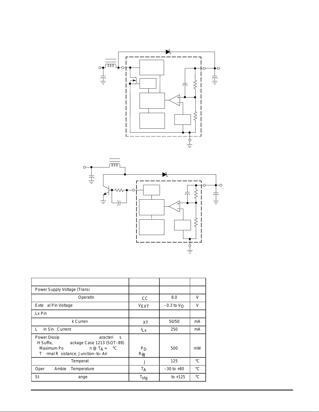
Representative Block Diagrams
MC33463H–XXKT1
D
L
V
in
3
Lx
C
in
VLx Limitier
Drive
VFM
Controller
2
Output
V
O
C
O
100 kHz
Oscillator
L
V
in
C
in
Q
Rb
Cb
This device contains 100 active transistors.
MC33463H–XXLT1
3
EXT
Drive
VFM
Controller
100 kHz
Oscillator
XX Denotes Output Voltage
V
ref
Gnd
1
D
V
2
Output
V
ref
Gnd1
O
C
O
MAXIMUM RATINGS (T
Power Supply Voltage (Transient)
Power Supply Voltage (Operating)
External Pin Voltage
Lx Pin Voltage
EXT Pin Source/Sink Current
Lx Pin Sink Current
Power Dissipation and Thermal Characteristics
H Suffix, Plastic Package Case 1213 (SOT–89)
Maximum Power Dissipation @ T
Thermal Resistance, Junction–to–Air R
Operating Junction Temperature
Operating Ambient Temperature
Storage Temperature Range
= 25°C, unless otherwise noted.)
C
Rating Symbol Value Unit
= 25°C P
A
2
V
V
V
I
CC
CC
EXT
V
Lx
EXT
I
Lx
D
θJA
T
J
T
A
T
stg
12
8.0
–0.3 to V
–30 to +80
–40 to +125
O
12
50/50
250
500 mW
200 °C/W
125
V
V
V
V
mA
mA
°C
°C
°C
MOTOROLA ANALOG IC DEVICE DATA
MC33463
ÁÁÁ
ÁÁÁ
ÁÁÁ
ÁÁÁ
ÁÁÁ
ÁÁÁ
ÁÁÁ
ÁÁÁ
ÁÁÁ
ÁÁÁ
ELECTRICAL CHARACTERISTICS (V
Characteristic
= 2.0 V, IO = 10 mA and TA = 25°C, unless otherwise noted.)
CC
Symbol Min Typ Max Unit
OSCILLAT OR
Frequency
Oscillator Minimum Supply Voltage (IO = 0 mA)
Oscillator Duty Ratio Each Cycle
V
f
osc
CC
D
80
65
100
–
0.7
75
Lx OUTPUT (KT1 SUFFIX)
ON State Sink Current (VLx = 0.4 V)
I
Lx
30KT1 Suffix 60 – –
33KT1 Suffix 63 – –
50KT1 Suffix 80 – –
VLx Voltage Limit (Note 1) V
OFF State Leakage Current (VLx = 6.0 V)
LxLim
I
LKG
0.65 0.8 1.0 V
–
–
EXT OUTPUT (LT1 SUFFIX)
ON State Source Current (V
= VO – 0.4 V)
EXT
I
source
30LT1 Suffix 1.5 – –
33LT1 Suffix 1.575 – –
50LT1 Suffix 2.0 – –
OFF State Sink Current (V
EXT
= 0.4 V)
I
sink
30LT1 Suffix 1.5 – –
33LT1 Suffix 1.575 – –
50LT1 Suffix 2.0 – –
TOTAL DEVICE
Output Voltage
V
O
30KT1 or 30LT1 Suf fix 2.925 3.0 3.075
33KT1 or 33LT1 Suf fix 3.218 3.3 3.383
50KT1 or 50LT1 Suf fix 4.875 5.0 5.125
Quiescent Bias Current (Vin = 2.0 V, IO = 0 mA)
I
Q
30KT1 Suffix – 4.0 8.0
33KT1 Suffix – 4.3 8.6
50KT1 Suffix – 6.0 12
Quiescent Bias Current (Vin = VO + 0.5 V, IO = 0 mA)
30KT1 Suffix – 1.2 5.0
33KT1 Suffix – 1.2 5.0
50KT1 Suffix – 2.0 5.0
Quiescent Bias Current (Vin = 2.0 V, IO = 0 mA)
I
Q
30LT1 Suffix – 30 50
33LT1 Suffix – 34.5 56
50LT1 Suffix – 60 90
Quiescent Bias Current (Vin = VO + 0.5 V, IO = 0 mA)
30LT1 Suffix – 1.2 5.0
33LT1 Suffix – 1.2 5.0
50LT1 Suffix – 2.0 5.0
NOTE: 1.When the Lx switch is turned on, ILx carried through the R
off by the Lx switch protection circuit.
of the Lx switch results in VLx. When VLx reaches V
DS(on)
, the Lx switch is turned
LxLim
120
0.8
85
0.5
kHz
V
%
mA
µA
mA
mA
V
µA
µA
MOTOROLA ANALOG IC DEVICE DATA
3
MC33463
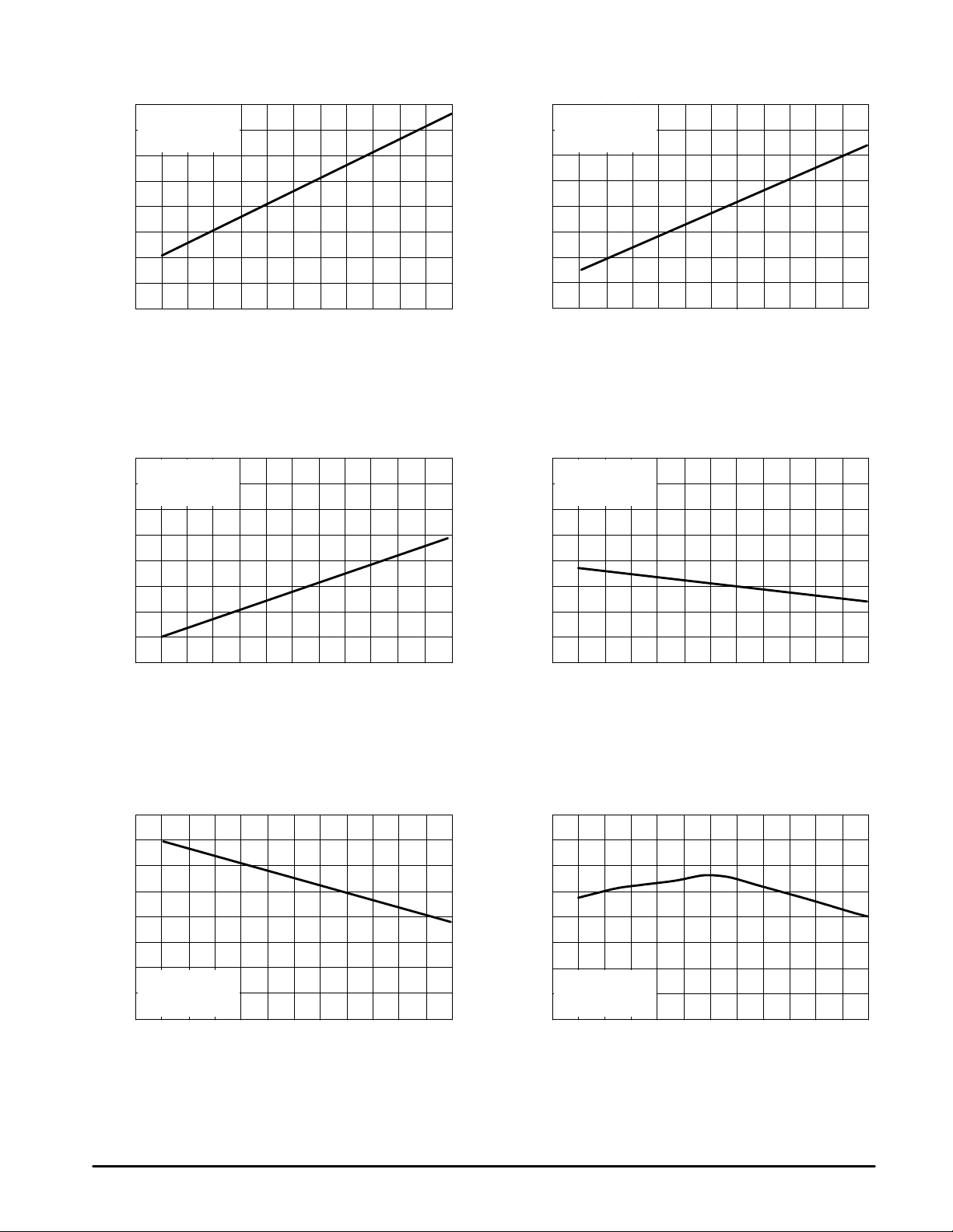
Figure 1. Quiescent Current versus T emperature
50
MC33463H–30LT1
µ
Vin = 2.0 V
IO = 0 mA
40
30
20
, QUIESCENT BIAS CURRENT ( A)
Q
I
10
–40
–20
0
TA, AMBIENT TEMPERATURE (°C)
20 40
60
Figure 3. Oscillator Frequency versus T emperature
200
MC33463H–50KT1
Vin = 2.0 V
IO = 10 mA
160
Figure 2. Quiescent Current versus T emperature
2.0
MC33463H–30KT1
µ
Vin = 3.5 V
IO = 0 mA
1.6
1.2
0.8
, QUIESCENT BIAS CURRENT ( A)
Q
I
0.4
80 –20
–40
100
MC33463H–50KT1
Vin = 2.0 V
IO = 10 mA
90
0
TA, AMBIENT TEMPERATURE (
20
40
°
C)
Figure 4. Oscillator Duty Ratio
versus T emperature
60
80
D, DUTY RATIO (%)
80
70
60
–40
–20
0
TA, AMBIENT TEMPERATURE (°C)
20
40
60
120
80
, OSCILLAT OR FREQUENCY (kHz)
osc
f
40
–40
–20
0
TA, AMBIENT TEMPERATURE (°C)
20
40
60
80
Figure 5. Lx Switching Current versus Temperature Figure 6. VLx V oltage Limit versus Temperature
200
160
120
80
, Lx SWITCHING CURRENT (mA)
MC33463H–50KT1
Lx
Vin = 2.0 V
I
IO = 10 mA
40
–40
–20
0
TA, AMBIENT TEMPERATURE (°C)
20
40
60
80
0.9
0.8
0.7
, Lx VOLTAGE LIMIT (V)
0.6
LxLim
MC33463H–50KT1
V
Vin = 2.0 V
IO = 10 mA
0.5
–40
–20
0
TA, AMBIENT TEMPERATURE (°C)
20
40
60
80
80
4
MOTOROLA ANALOG IC DEVICE DATA
 Loading...