

Motorola MC330076P2, MC330076D, MC330076P1 Datasheet
SEMICONDUCTOR
TECHNICAL DATA
DUAL HIGH OUTPUT
CURRENT OPERATIONAL
AMPLIFIER
Order this document by MC33076/D
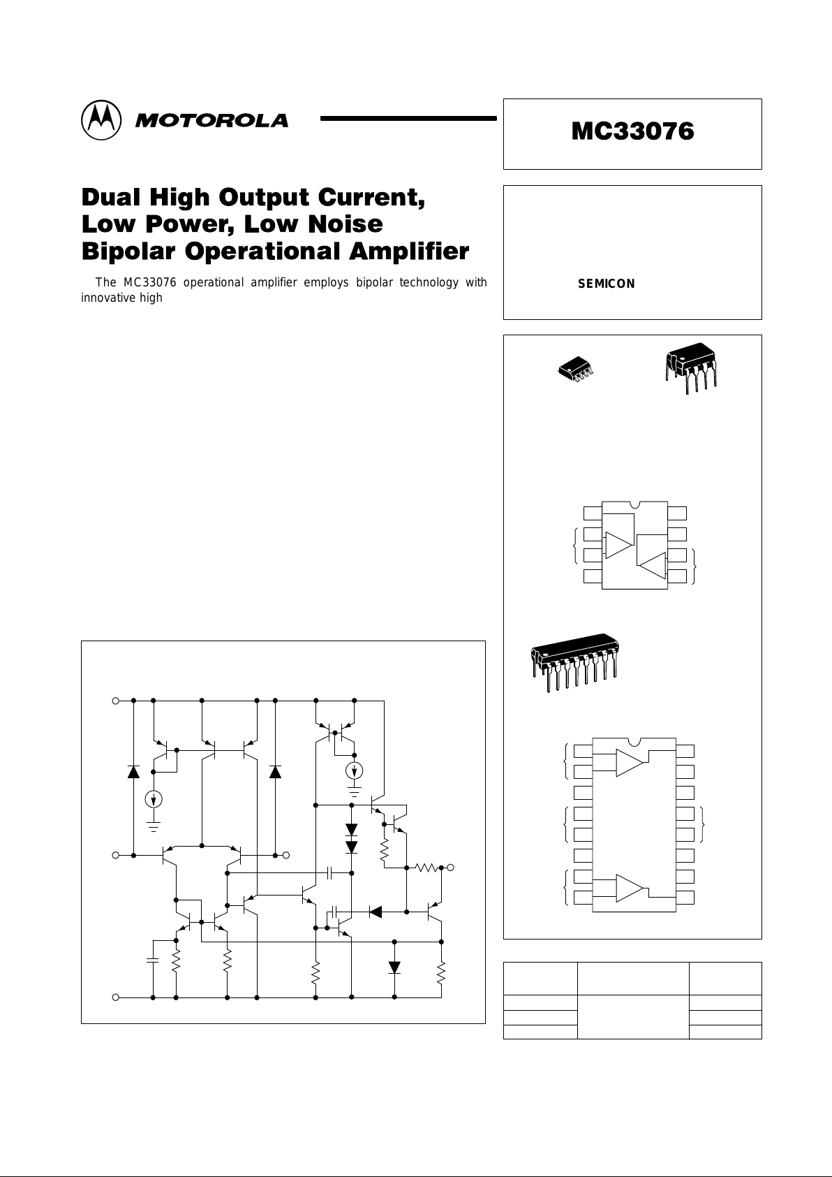
PIN CONNECTIONS
(8 Pin Pkg, Top View)
D SUFFIX
PLASTIC PACKAGE
CASE 751
(SO–8)
16
15
14
13
12
11
10
9
Inputs 1
1
2
3
4
5
6
7
8
NC
NC
V
EE
Inputs 2
Output 1
NC
V
CC
V
EE
NC
NC
Output 2
PIN CONNECTIONS
(16 Pin Pkg, Top View)
+
–
2
–
+
1
8
1
8
1
P1 SUFFIX
PLASTIC PACKAGE
CASE 626
16
1
P2 SUFFIX
PLASTIC PACKAGE
CASE 648C
DIP (12+2+2)
8
7
6
5
Inputs 1
1
2
3
4
Output 1
V
EE
Output 2
V
CC
Inputs 2
–
+
1
–
+
2
ORDERING INFORMATION
Device
Operating
Temperature Range
Package
MC33076D
TA = –40° to +85°C
SO–8
MC33076P1 Plastic DIP
MC33076P2 Power Plastic
1
MOTOROLA ANALOG IC DEVICE DATA
The MC33076 operational amplifier employs bipolar technology with
innovative high performance concepts for audio and industrial applications.
This device uses high frequency PNP input transistors to improve frequency
response. In addition, the amplifier provides high output current drive
capability while minimizing the drain current. The all NPN output stage
exhibits no deadband crossover distortion, large output voltage swing,
excellent phase and gain margins, low open loop high frequency output
impedance and symmetrical source and sink AC frequency performance.
The MC33076 is tested over the automotive temperature range and is
available in an 8–pin SOIC package (D suffix) and in both the standard 8 pin
DIP and 16–pin DIP packages for high power applications.
• 100 Ω Output Drive Capability
• Large Output Voltage Swing
• Low Total Harmonic Distortion
• High Gain Bandwidth: 7.4 MHz
• High Slew Rate: 2.6 V/µs
• Dual Supply Operation: ±2.0 V to ±18 V
• High Output Current: ISC = 250 mA typ
• Similar Performance to MC33178
Equivalent Circuit Schematic
(Each Amplifier)
V
in+
V
CC
V
in–
V
EE
I
ref
I
ref
C
C
C
M
V
out
Motorola, Inc. 1996 Rev 0
MC33076
2
MOTOROLA ANALOG IC DEVICE DATA
MAXIMUM RATINGS
Rating Symbol Value Unit
Power Supply Voltage (Note 2) VCC to
V
EE
+36 V
Input Differential Voltage Range V
IDR
(Note 1) V
Input Voltage Range V
IR
(Note 1) V
Output Short Circuit Duration (Note 2) t
SC
5.0 sec
Maximum Junction Temperature T
J
+150 °C
Storage Temperature T
stg
–60 to +150 °C
Maximum Power Dissipation P
D
(Note 2) mW
NOTES: 1. Either or both input voltages should not exceed VCC or VEE.
2.Power dissipation must be considered to ensure maximum junction temperature (TJ)
is not exceeded (see power dissipation performance characteristic, Figure 1).
See applications section for further information.
DC ELECTRICAL CHARACTERICISTICS (V
CC
= +15 V , VEE = –15 V , TA = 25°C, unless otherwise noted.)
Characteristics Figure Symbol Min Typ Max Unit
Input Offset Voltage (RS = 50 Ω, VCM = 0 V)
(VS = ±2.5 V to ±15 V)
TA = +25°C
TA = –40° to +85°C
2 |VIO|
—
—
0.5
0.5
4.0
5.0
mV
Input Offset Voltage Temperature Coefficient
(RS = 50 Ω, VCM = 0 V)
TA = –40° to +85°C
∆VIO/∆T
— 2.0 —
µV/°C
Input Bias Current (VCM = 0 V)
TA = +25°C
TA = –40° to +85°C
3, 4 I
IB
—
—
100
—
500
600
nA
Input Offset Current (VCM = 0 V)
TA = +25°C
TA = –40° to +85°C
|IIO|
—
—
5.0
—
70
100
nA
Common Mode Input Voltage Range 5 V
ICR
–13 –14
+14
13
V
Large Signal Voltage Gain (VO = –10 V to +10 V)
(TA = +25°C)
RL = 100 Ω
RL = 600 Ω
(TA = –40° to +85°C)
RL = 600 Ω
6 A
VOL
25
50
25
—
200
—
—
—
—
kV/V
Output Voltage Swing (VID = ±1.0 V)
(VCC = +15 V , VEE = –15 V)
RL = 100 Ω
RL = 100 Ω
RL = 600 Ω
RL = 600 Ω
(VCC = +2.5 V , VEE = –2.5 V)
RL = 100 Ω
RL = 100 Ω
7, 8, 9
V
O+
V
O–
V
O+
V
O–
V
O+
V
O–
10
—
13
—
1.2
—
+11.7
–11.7
+13.8
–13.8
+1.66
–1.74
—
–10
—
–13
—
–1.2
V
Common Mode Rejection (Vin = ±13 V) 10 CMR 80 116 — dB
Power Supply Rejection
(VCC/VEE = +15 V/–15 V , +5.0 V/–15 V, +15 V/–5.0 V)
11 PSR
80 120 —
dB
MC33076
3
MOTOROLA ANALOG IC DEVICE DATA
DC ELECTRICAL CHARACTERICISTICS (V
CC
= +15 V , VEE = –15 V , TA = 25°C, unless otherwise noted.)
Characteristics Figure Symbol Min Typ Max Unit
Output Short Circuit Current (VID = ±1.0 V Output to Gnd)
(VCC = +15 V , VEE = –15 V)
Source
Sink
(VCC = +2.5 V , VEE = –2.5 V)
Source
Sink
12, 13 I
SC
190
—
63
—
+250
–280
+94
–80
—
–215
—
–46
mA
Power Supply Current per Amplifier (VO = 0 V)
(VS = ±2.5 V to ±15 V)
TA = +25°C
TA = –40° to +85°C
14 I
D
—
—
2.2
—
2.8
3.3
mA
AC ELECTRICAL CHARACTERICISTICS (V
CC
= +15 V , VEE = –15 V , TA = 25°C, unless otherwise noted.)
Characteristics
Figure Symbol Min Typ Max Unit
Slew Rate (Vin = –10 V to +10 V, RL = 100 Ω, CL = 100 pF, AV = +1) 15 SR 1.2 2.6 — V/µs
Gain Bandwidth Product (f = 20 kHz) 16 GBW 4.0 7.4 — MHz
Unity Gain Frequency (Open Loop) (RL = 600 Ω, CL = 0 pF) — f
U
— 3.5 — MHz
Gain Margin (RL = 600 Ω, CL = 0 pF) 19, 20 A
m
— 15 — dB
Phase Margin (RL = 600 Ω, CL = 0 pF) 19, 20 ∅
m
— 52 — Deg
Channel Separation (f = 100 Hz to 20 kHz) 21 CS — –120 — dB
Power Bandwidth (VO = 20 Vpp, RL = 600 Ω, THD ≤1%) — BW
p
— 32 — kHz
Total Harmonic Distortion (RL = 600 Ω, VO = 2.0 Vpp, AV = +1)
f = 1.0 kHz
f = 10 kHz
f = 20 kHz
22 THD
—
—
—
0.0027
0.011
0.022
—
—
—
%
Open Loop Output Impedance (VO = 0 V, f = 2.5 MHz, AV = 10) 23 |ZO| — 75 — Ω
Differential Input Resistance (VCM = 0 V) — R
in
— 200 — kΩ
Differential Input Capacitance (VCM = 0 V) — C
in
— 10 — pF
Equivalent Input Noise Voltage (RS = 100 Ω)
f = 10 Hz
f = 1.0 kHz
24 e
n
—
—
7.5
5.0
—
nV/√Hz
Equivalent Input Noise Current
f = 10 Hz
f = 1.0 kHz
— i
n
—
—
0.33
0.15
—
—
pA/√Hz
MC33076
4
MOTOROLA ANALOG IC DEVICE DATA
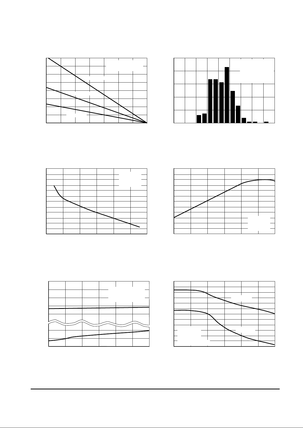
Figure 1. Maximum Power Dissipation
versus Temperature
, MAXIMUM POWER DISSIPATION (mW)
–60 –30
TA, AMBIENT TEMPERATURE (
°
C)
MC33076P2
MC33076P1
MC33076D
See Application Section
for Further Information
PERCENTAGE OF AMPLIFIERS (%)
Figure 2. Distribution of Input
Offset Voltage
VIO, INPUT OFFSET VOLTAGE (mV)
Figure 3. Input Bias Current versus
Common Mode Voltage
VCM, COMMON MODE VOLTAGE (V)
I , INPUT BIAS CURRENT (nA)
IB
I , INPUT BIAS CURRENT (nA)
IB
Figure 4. Input Bias Current
versus Temperature
TA, AMBIENT TEMPERATURE (°C)
A
Figure 5. Input Common Mode Voltage
Range versus Temperature
TA, TEMPERATURE (°C)
Figure 6. Open Loop Voltage Gain
versus Temperature
TA, AMBIENT TEMPERATURE (°C)
P
D
VOL
, OPEN LOOP VOL TAGE GAIN (dB)
4000
3500
3000
2500
2000
1500
1000
500
0
25
20
15
10
5
0
250
225
200
175
150
125
100
150
137
125
112
100
88
75
V
EE
120
115
110
105
100
95
90
VCC–1.0
VEE+0.125
VEE+0.25
VCC–0.75
VCC–0.50
VCC–0.25
V
CC
0 30 60 90 120 150 –2.0 –1.5 –1.0 –0.5 0 0.5 1.0 1.5 2.0
–15 –10 –5.0 0 5.0 10 15 –55 –25 5.0 35 65 95 125
–55 –25 5.0 35 65 95 125
–55 –25 5.0 35 65 95 125
2.5
180 amplifiers tested
from 3 wafer lots
VCC =
±
15 V
TA = 25
°
C
(Plastic DIP package)
VCC = +15 V
VEE = –15 V
TA = 25
°
C
VCC = +15 V
VEE = –15 V
VCM = 0 V
VCC = +5.0 V to +18 V
VEE = –5.0 V to –18 V
∆
VIO = 5.0 mV
RL = 2.0 k
Ω
RL = 100
Ω
VCC = +
15 V
VEE = –15 V
f = 10 Hz
∆
VO = –10 to +10 V
 Loading...