

Device
Operating
Temperature Range
Package
SEMICONDUCTOR
TECHNICAL DATA
LOW POWER
FM TRANSMITTER
SYSTEM
ORDERING INFORMATION
MC2833D
MC2833P
TA = – 30 to +75°C
SO–16
Plastic DIP
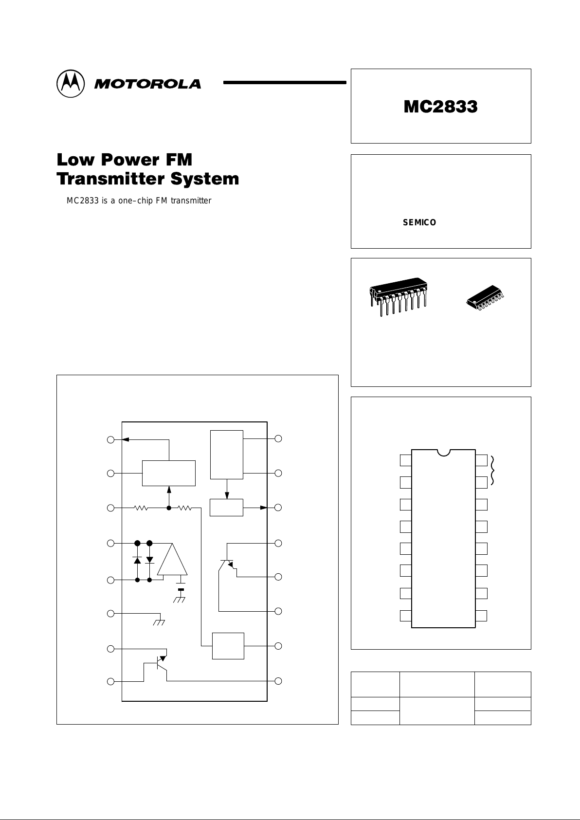
PIN CONNECTIONS
Order this document by MC2833/D
D SUFFIX
PLASTIC PACKAGE
CASE 751B
(SO–16)
P SUFFIX
PLASTIC PACKAGE
CASE 648
Tr 1
Base
Tr 1
Emitter
Gnd
Mic Amp
Input
9
10
11
12
13
14
15
16
8
7
6
5
4
3
2
1
Variable
Reactance
Output
Decoupling
Modulator
Input
Mic Amp
Output
Tr 1
Collector
V
CC
Tr 2
Collector
Tr 2
Emitter
Tr 2
Base
RF
Output
RF
Osc
1
MOTOROLA ANALOG IC DEVICE DATA
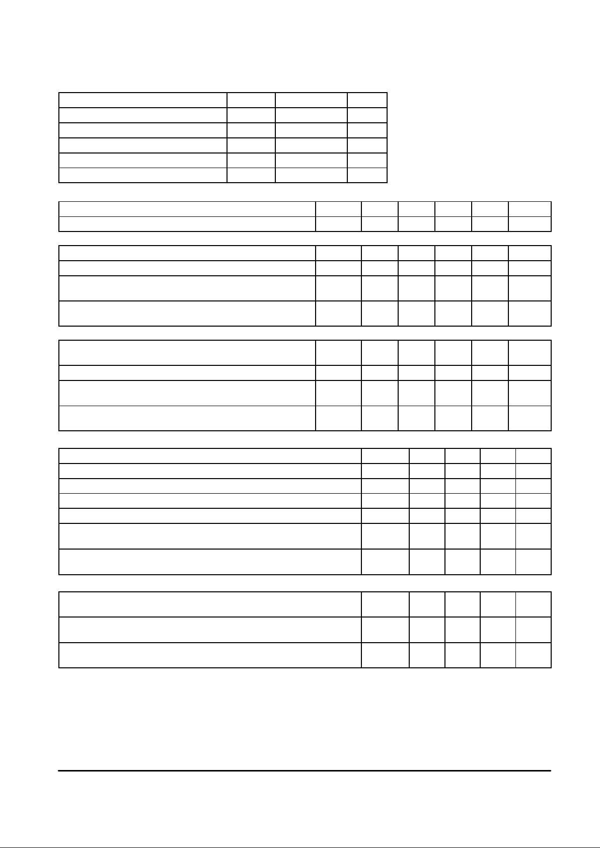
MC2833 is a one–chip FM transmitter subsystem designed for cordless
telephone and FM communication equipment. It includes a microphone
amplifier, voltage controlled oscillator and two auxiliary transistors.
• Wide Range of Operating Supply Voltage (2.8–9.0 V)
• Low Drain Current (I
CC
= 2.9 mA Typ)
• Low Number of External Parts Required
• – 30 dBm Power Output to 60 MHz Using Direct RF Output
• +10 dBm Power Output Attainable Using On–Chip Transistor Amplifiers
• Users Must Comply with Local Regulations on R.F.
Transmission (FCC, DOT, P.T.T., etc)
Representative Block Diagram
+–
2
16
15
14
13
12
11
10
9
8
7
6
5
4
3
1
Variable
Reactance
RF
Osc
Buffer
Mic
Amp
V
REF
Motorola, Inc. 1996 Rev 1
MC2833
2
MOTOROLA ANALOG IC DEVICE DATA
MAXIMUM RATINGS
Ratings Symbol Value Unit
Power Supply Voltage V
CC
10 (max) V
Operating Supply Voltage Range V
CC
2.8–9.0 V
Junction Temperature T
J
+ 150 °C
Operating Ambient Temperature T
A
– 30 to + 75 °C
Storage Temperature Range T
stg
– 65 to + 150 °C
ELECTRICAL CHARACTERISTICS (V
CC
= 4.0 V, TA = 25°C, unless otherwise noted)
Characteristics
Symbol Pin Min Typ Max Unit
Drain Current (No input signal) I
CC
10 1.7 2.9 4.3 mA
FM MODULATOR
Output RF Voltage (fo = 16.6 MHz) V
out
RF 14 60 90 130 mVrms
Output DC Voltage (No input signal) Vdc 14 2.2 2.5 2.8 V
Modulation Sensitivity (fo = 16.6 MHz)
Modulation Sensitivity (Vin = 0.8 V to 1.2 V)
SEN 3
14
7.0
–
10
–
15–Hz/mVdc
Maximum Deviation (fo = 16.6 MHz)
Maximum Deviation (Vin = 0 V to 2.0 V)
Fdev 3
14
3.0
–
5.0
–
10
–
kHz
MIC AMPLIFIER
Closed Loop Voltage Gain (Vin = 3.0 mVrms)
Closed Loop Voltage Gain (fin = 1.0 kHz)
A
v
4
5
27
–
30
–
33
–
dB
Output DC Voltage (No input signal) V
out
dc 4 1.1 1.4 1.7 V
Output Swing Voltage (Vin = 30 mVrms)
Output Swing Voltage (fin = 1.0 kHz)
V
out
p–p 4 0.8 1.2 1.6 Vp–p
Total Harmonic Distortion (Vin = 3.0 mVrms)
Total Harmonic Distortion (fin = 1.0 kHz)
THD 4 – 0.15 2.0 %
AUXILIARY TRANSISTOR STATIC CHARACTERISTICS
Characteristics Symbol Min Typ Max Unit
Collector Base Breakdown Voltage (IC = 5.0 µA) V
(BR)CBO
15 45 – V
Collector Emitter Breakdown Voltage (IC = 200 µA) V
(BR)CEO
10 15 – V
Collector Substrate Breakdown Voltage (IC = 50 µA) V
(BR)CSO
– 70 – V
Emitter Base Breakdown Voltage (IE = 50 µA) V
(BR)EBO
– 6.2 – V
Collector Base Cut Off Current (VCB = 10 V)
Collector Base Cut Off Current (IE = 0)
I
CBO
– – 200 nA
DC Current Gain (IC = 3.0 mA)
DC Current Gain (VCE = 3.0 V)
h
FE
40 150 – –
AUXILIARY TRANSISTOR DYNAMIC CHARACTERISTICS
Current Gain Bandwidth Product (VCE = 3.0 V)
Current Gain Bandwidth Product (IC = 3.0 mA)
f
T
– 500 – MHz
Collector Base Capacitance (VCE = 3.0 V)
Collector Base Capacitance (IC = 0)
C
CB
– 2.0 – pF
Collector Substrate Capacitance (VCS = 3.0 V)
Collector Substrate Capacitance (IC = 0)
C
CS
– 3.3 – pF
MC2833
3
MOTOROLA ANALOG IC DEVICE DATA
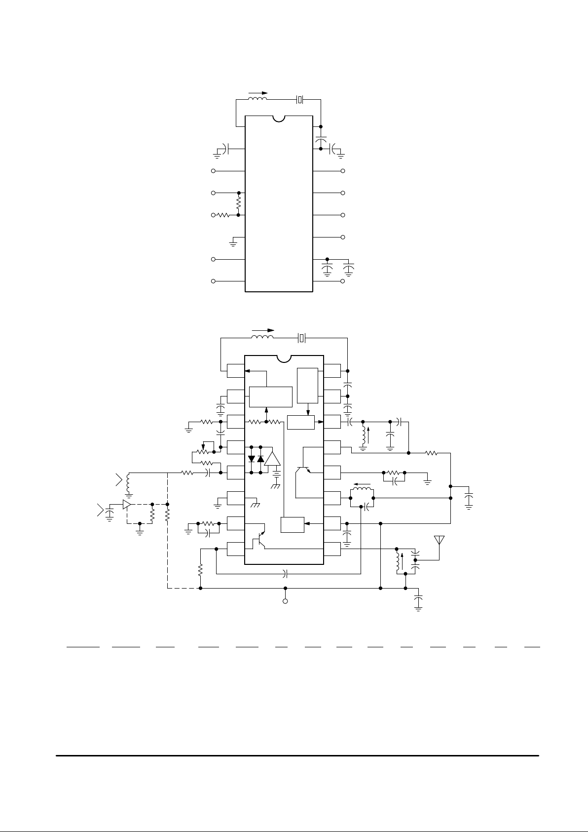
Figure 1. Test Circuit
Figure 2. Single Chip VHF Narrowband FM Transmitter
Electret
(alternate)
Microphone
and biasing
470 p
1.0
µ
F
tantalum
+
1000 p
C5
RF Output
5.0 to 10 dBm
(see Note 4)
C4
C3
L1
L2
C2
1.0 k
390 k
0.22
µ
C1
Cc1
47 p
Q2
Cc2
V
CC
= 9.0 Vdc
Rb1
470 p
Q1
Re1
2.7 k
4.7 k
Dynamic
Mike
Audio
Input
100 k
Deviation
Adjust
120 k
X1Lt
1.0 k
56 p
51 p
V
REF
Buffer
RF
Osc.
Variable
Reactance
Mic Amp
9
16
15
14
13
12
1
2
3
4
5
6
7
8
10
11
+–
1.0
µ
100 k
4700 p
4700 p
Crystal:
39 pF
68 pF
+
47
µ
F
0.01
µ
F
Collector 1
Collector 2
Base 2
Emitter 2
Base 1
Emitter 1
Mic Amp
Out
RF Out
0.0047
µ
F
Mod Out
16.605 MHz
5.1
µ
H
Mod In
Mic Amp
In
220 k
6.3 k
MC2833
6
7
1
2
3
4
5
89
10
11
12
13
14
15
16
f
o
C
L
C
o
R
S
= 16.605 MHz
= 30 pF
= 6.1 pF
= 10 Ω Max
NOTES:
1. Components versus output frequency:
Output RF
X1 (MHz) Lt (µH) L1 (µH) L2 (µH) Re1 Rb1 Cc1 Cc2 C1 C2 C3 C4 C5
49.7 MHz
76 MHz
144.6 MHz
16.5667
12.6000
12.05
3.3–4.7
5.1
5.6
0.22
0.22
0.15
0.22
0.22
0.10
330
150
150
390 k
300 k
220 k
33 p
68 p
47 p
33 p
10 p
10 p
33 p
68 p
68 p
470 p
470 p
1000 p
33 p
12 p
18 p
47 p
20 p
12 p
220 p
120 p
33 p
2. Crystal X1 is fundamental mode, calibrated for parallel resonance with a 32 pF load. The final output frequency is generated by frequency multiplication within
2. the MC2833 IC. The RF output buffer (Pin 14) and Q2 transistor are used as a frequency tripler and doubler, respectively, in the 76 and 144.6 MHz transmitters.
2. The Q1 output transistor is a linear amplifier in the 49.7 MHz and 76 MHz transmitters, and a frequency doubler in the 144.6 MHz transmitter.
3. All coils used are 7 mm shielded inductors, CoilCraft series M1 175A, M1282A–M1289A, M1312A or equivalent.
4. Power output is ≈ + 10 dBm for 49.7 MHz and 76 MHz transmitters, and ≈ + 5.0 dBm for the 144.6 MHz transmitter at VCC = 8.0 V. Power output drops with
4. lower VCC.
5. All capacitors in microfarads, inductors in Henries and resistors in Ohms unless otherwise specified.
6. Other frequency combinations may be set–up by simple scaling of the 3 examples shown.
 Loading...