

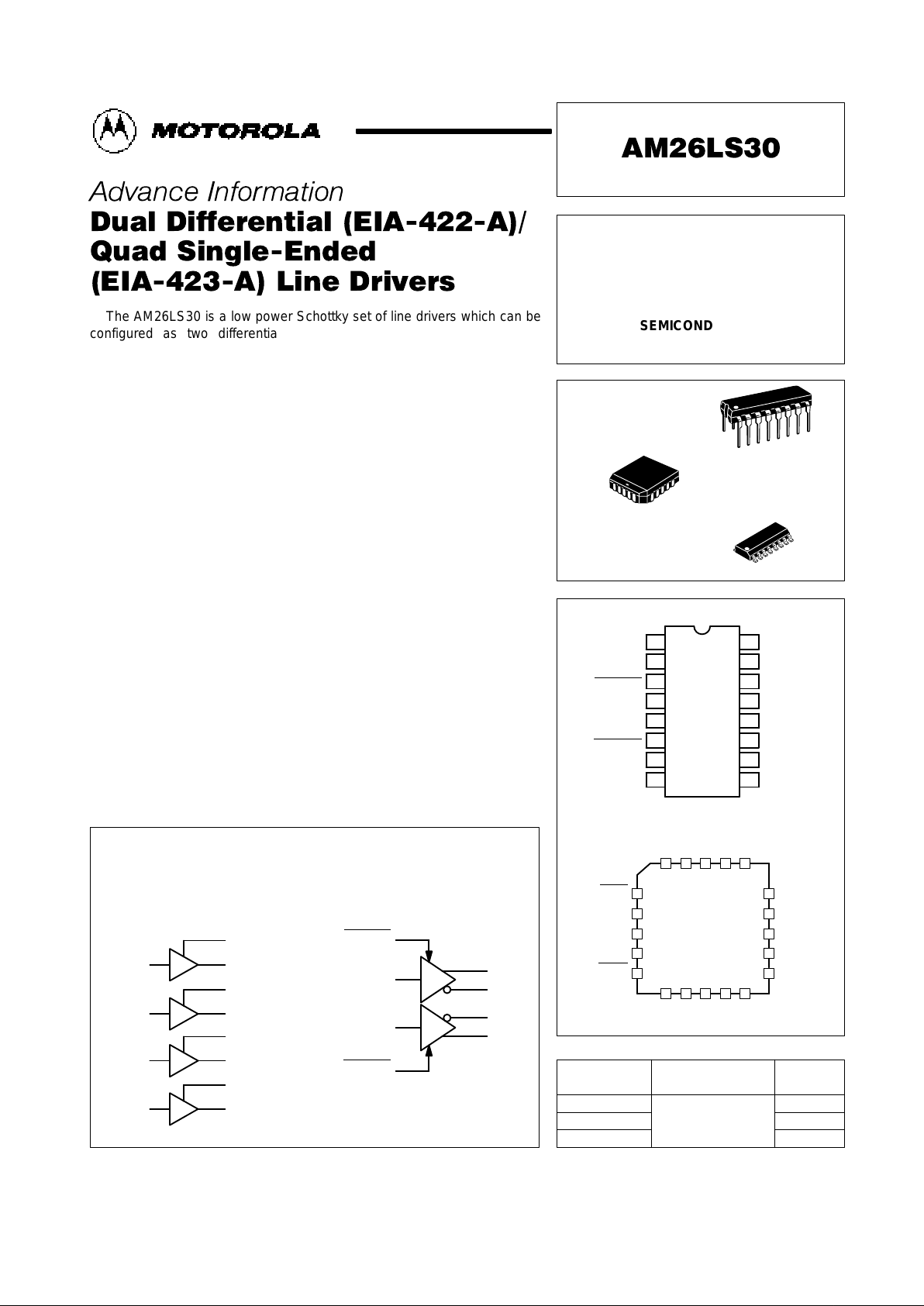
Device
Operating
Temperature Range
Package
SEMICONDUCTOR
TECHNICAL DATA
DUAL DIFFERENTIAL/
QUAD SINGLE–ENDED
LINE DRIVERS
ORDERING INFORMATION
AM26LS30PC
MC26LS30D TA = – 40° to +85°C
Plastic DIP
SO–16
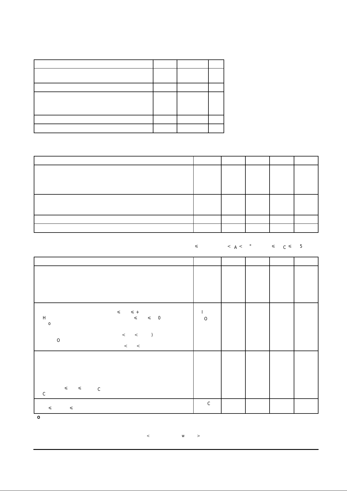
PIN CONNECTIONS
Order this document by AM26LS30/D
PC SUFFIX
PLASTIC PACKAGE
CASE 648
D SUFFIX
PLASTIC PACKAGE
CASE 751B
(SO–16)
FN SUFFIX
PLASTIC PACKAGE
CASE 775
AM26LS30FN PLCC–20
In B/En AB
Mode
NC
Gnd
In C/En CD
Out B
SR–B
NC
SR–C
Out C
Input A
VCCNC
SR–A
Out A
In D
NC
SR–D
Out D
V
EE
4
5
6
7
8
18
17
16
15
14
3 2 1 20 19
9 10 11 12 13
16
1
4
2
5
6
7
8
9
3
10
11
12
13
14
15
Input C/
Enable CD
(Top View)
SR–A
Output A
Output B
Input D
V
EE
SR–D
Output D
Output C
SR–C
SR–B
Gnd
V
CC
Input A
Mode
Input B/
Enable AB
1
MOTOROLA ANALOG IC DEVICE DATA
The AM26LS30 is a low power Schottky set of line drivers which can be
configured as two differential drivers which comply with EIA–422–A
standards, or as four single–ended drivers which comply with EIA–423–A
standards. A mode select pin and appropriate choice of power supplies
determine the mode. Each driver can source and sink currents in excess of
50 mA.
In the differential mode (EIA–422–A), the drivers can be used up to
10 Mbaud. A disable pin for each driver permits setting the outputs into a
high impedance mode within a ±10 V common mode range.
In the single–ended mode (EIA–423–A), each driver has a slew rate
control pin which permits setting the slew rate of the output signal so as to
comply with EIA–423–A and FCC requirements and to reduce crosstalk.
When operated from symmetrical supplies (±5.0 V), the outputs exhibit zero
imbalance.
The AM26LS30 is available in a 16–pin plastic DIP and surface mount
package. Operating temperature range is –40° to +85°C.
• Operates as Two Differential EIA–422–A Drivers, or Four Single–Ended
EIA–423–A Drivers
• High Impedance Outputs in Differential Mode
• Short Circuit Current Limit In Both Source and Sink Modes
• ± 10 V Common Mode Range on High Impedance Outputs
• ± 15 V Range on Inputs
• Low Current PNP Inputs Compatible with TTL, CMOS, and MOS
Outputs
• Individual Output Slew Rate Control in Single–Ended Mode
• Replacement for the AMD AM25LS30 and National Semiconductor
DS3691
Representative Block Diagrams
Single–Ended Mode
EIA–423–A
Differential Mode
EIA–422–A
Enable CD
Enable AB
Out D
Out C
Out B
Out A
VCC–1
VEE–8
Input D
Input A
Input A
SR–A
Out A
Gnd–5
Mode–4
SR–B
SR–C
Out D
SR–D
Out C
Out B
Input B
Input C
Input D
Motorola, Inc. 1995This document contains information on a new product. Specifications and information herein are
subject to change without notice.
AM26LS30
2
MOTOROLA ANALOG IC DEVICE DATA
MAXIMUM OPERATING CONDITIONS
(Pin numbers refer to DIP and SO–16
packages only.)
Rating
Symbol Value Unit
Power Supply Voltage V
CC
V
EE
–0.5, +7.0
–7.0, +0.5
Vdc
Input Voltage (All Inputs) V
in
–0.5, +20 Vdc
Applied Output Voltage when in High Impedance Mode
(VCC = 5.0 V, Pin 4 = Logic 0, Pins 3, 6 = Logic 1)
V
za
±15 Vdc
Output Voltage with VCC, VEE = 0 V V
zb
±15
Output Current I
O
Self limiting –
Junction Temperature T
J
–65, +150 °C
Devices should not be operated at these limits. The “Recommended Operating Conditions” table provides
conditions for actual device operation.
RECOMMENDED OPERATING CONDITIONS
Rating Symbol Min Typ Max Unit
Power Supply Voltage (Differential Mode) V
CC
V
EE
+4.75
–0.5
5.0
0
+5.25
+0.3
Vdc
Power Supply Voltage (Single–Ended Mode) V
CC
V
EE
+4.75
–5.25
+5.0
–5.0
+5.25
–4.75
Input Voltage (All Inputs) V
in
0 – +15 Vdc
Applied Output Voltage (when in High Impedance Mode) V
za
–10 – +10
Applied Output Voltage, VCC = 0 V
zb
–10 – +10
Output Current I
O
–65 – +65 mA
Operating Ambient Temperature (See text) T
A
–40 – +85 °C
All limits are not necessarily functional concurrently.
ELECTRICAL CHARACTERISTICS (EIA–422–A differential mode, Pin 4
p
0.8 V, –40°C tTA t85°C, 4.75 V p VCC p 5.25 V,
VEE = Gnd, unless otherwise noted. Pin numbers refer to DIP and SO–16 packages only.)
Characteristic
Symbol Min Typ Max Unit
Output Voltage (see Figure 1)
Differential, RL = ∞, VCC = 5.25 V
Differential, RL = 100 Ω, VCC = 4.75 V
Change in Differential Voltage, RL = 100 Ω (Note 4)
Offset Voltage, RL = 100 Ω
Change in Offset Voltage*, RL = 100 Ω
V
OD1
V
OD2
∆V
OD2
V
OS
∆VOS
–
2.0
–
–
–
4.2
2.6
10
2.5
10
6.0
–
400
3.0
400
Vdc
Vdc
mVdc
Vdc
mVdc
Output Current (each output)
Power Off Leakage, VCC = 0, –10 V p VO p +10 V
High Impedance Mode, VCC = 5.25 V, –10 V p VO p +10 V
Short Circuit Current (Note 2)
High Output Shorted to Pin 5 (TA = 25°C)
High Output Shorted to Pin 5 (–40°C t TA t+85°C)
Low Output Shorted to +6.0 V (TA = 25°C)
Low Output Shorted to +6.0 V (–40°C t TA t +85°C)
I
OLK
I
OZ
I
SC–
I
SC–
I
SC+
I
SC+
–100
–100
–150
–150
60
50
0
0
–95
–
75
–
+100
+100
–60
–50
150
150
µA
mA
Inputs
Low Level Voltage
High Level Voltage
Current @ Vin = 2.4 V
Current @ Vin = 15 V
Current @ Vin = 0.4 V
Current, 0 p Vin p 15 V, VCC = 0
Clamp Voltage (Iin = –12 mA)
V
IL
V
IH
I
IH
I
IHH
I
IL
I
IX
V
IK
–
2.0
–
–
–200
–
–1.5
–
–
0
0
–8.0
0
–
0.8
–
40
100
–
–
–
Vdc
Vdc
µA
Vdc
Power Supply Current (VCC = +5.25 V, Outputs Open)
(0 p Enable p VCC)
I
CC
– 16 30
mA
NOTES: 1. All voltages measured with respect to Pin 5.
2.Only one output shorted at a time, for not more than 1 second.
3.Typical values established at +25°C, VCC = +5.0 V, VEE = –5.0 V.
4.Vin switched from 0.8 to 2.0 V.
5.Imbalance is the difference between VO2 with Vin t 0.8 V and VO2 with Vin u 2.0 V.
AM26LS30
3
MOTOROLA ANALOG IC DEVICE DATA
TIMING CHARACTERISTICS (EIA–422–A differential mode, Pin 4
p
0.8 V, TA = 25°C, VCC = 5.0 V, VEE = Gnd, (Notes 1 and 3)
unless otherwise noted.)
Characteristic
Symbol Min Typ Max Unit
Differential Output Rise Time (Figure 3) t
r
– 70 200 ns
Differential Output Fall Time (Figure 3) t
f
– 70 200 ns
Propagation Delay Time – Input to Differential Output
Input Low to High (Figure 3)
Input High to Low (Figure 3)
t
PDH
t
PDL
–
–
90
90
200
200
ns
Skew Timing (Figure 3)
t
PDH
to t
PDL
for Each Driver
Max to Min t
PDH
Within a Package
Max to Min t
PDL
Within a Package
t
SK1
t
SK2
t
SK3
–
–
–
9.0
2.0
2.0
–
–
–
ns
Enable Timing (Figure 4)
Enable to Active High Differential Output
Enable to Active Low Differential Output
Enable to 3–State Output From Active High
Enable to 3–State Output From Active Low
t
PZH
t
PZL
t
PHZ
t
PLZ
–
–
–
–
150
190
80
110
300
350
350
300
ns
ELECTRICAL CHARACTERISTICS (EIA–423–A single–ended mode, Pin 4
q
2.0 V, –40°C t TA t 85°C, 4.75 V p V
CC
,
|V
EE
p
5.25 V, (Notes 1 and 3) unless otherwise noted).
Characteristic
Symbol Min Typ Max Unit
Output Voltage (VCC = VEE = 4.75 V)
Single–Ended Voltage, RL = ∞ (Figure 2)
Single–Ended Voltage, RL = 450 Ω, (Figure 2)
Voltage Imbalance (Note 5), RL = 450 Ω
VO1
VO2
∆VO2
4.0
3.6
–
4.2
3.95
0.05
6.0
6.0
0.4
Vdc
Slew Control Current (Pins 16, 13, 12, 9) I
SLEW
– ±120 – µA
Output Current (Each Output)
Power Off Leakage, VCC = VEE = 0, –6.0 V p VO p +6.0 V
Short Circuit Current (Output Short to Ground, Note 2)
Vin p 0.8 V (TA = 25°C)
Vin p 0.8 V (–40°C t TA t +85°C)
Vin w 2.0 V (TA = 25°C)
Vin w 2.0 V (–40°C t TA t +85°C)
I
OLK
I
SC+
I
SC+
I
SC–
I
SC–
–100
60
50
–150
–150
0
80
–
–95
–
+100
150
150
–60
–50
µA
mA
Inputs
Low Level Voltage
High Level Voltage
Current @ Vin = 2.4 V
Current @ Vin = 15 V
Current @ Vin = 0.4 V
Current, 0 p Vin p 15 V, VCC = 0
Clamp Voltage (Iin = –12 mA)
V
IL
V
IH
I
IH
I
IHH
I
IL
I
IX
V
IK
–
2.0
–
–
–200
–
–1.5
–
–
0
0
–8.0
0
–
0.8
–
40
100
–
–
–
Vdc
Vdc
µA
Vdc
Power Supply Current (Outputs Open)
VCC = +5.25 V, VEE = –5.25 V, Vin = 0.4 V
I
CC
I
EE
–
–22
17
–8.0
30
–
mA
TIMING CHARACTERISTICS (EIA–423–A single–ended mode, Pin 4
q
2.0 V, TA = 25°C, VCC = 5.0 V, VEE = –5.0 V, (Notes 1 and 3)
unless otherwise noted.)
Characteristic
Symbol Min Typ Max Unit
Output Timing (Figure 5)
Output Rise Time, CC = 0
Output Fall Time, CC = 0
Output Rise Time, CC = 50 pF
Output Fall Time, CC = 50 pF
t
r
t
f
t
r
t
f
–
–
–
–
65
65
3.0
3.0
300
300
–
–
ns
µs
Rise Time Coefficient (Figure 16) C
rt
– 0.06 – µs/pF
Propagation Delay Time, Input to Single Ended Output (Figure 5)
Input Low to High, CC = 0
Input High to Low, CC = 0
t
PDH
t
PDL
–
–
100
100
300
300
ns
Skew Timing, CC = 0 (Figure 5)
t
PDH
to t
PDL
for Each Driver
Max to Min t
PDH
Within a Package
Max to Min t
PDL
Within a Package
t
SK4
t
SK5
t
SK6
–
–
–
15
2.0
5.0
–
–
–
ns
AM26LS30
4
MOTOROLA ANALOG IC DEVICE DATA
Table 1
Inputs Outputs
Operation V
CC
V
EE
Mode A B C D A B C D
Differential
+5.0 Gnd 0
0
0
0
0
0
1
1
0
(EIA–422–A) 0
1
0
0
1
1
0
0
1
0
X
1
0
1
Z
Z
0
1
010001010
000010101
0101X10ZZ
Single–Ended
+5.0 –5.0 1
0
0
0
0
0
0
0
0
(EIA–423–A) 1
1
0
0
0
1
0
0
0
1
0
1
0
0
0
1
0
0
100100010
100010001
X 0 X X X X X X Z Z Z Z
X = Don’t Care
Z = High Impedance (Off)
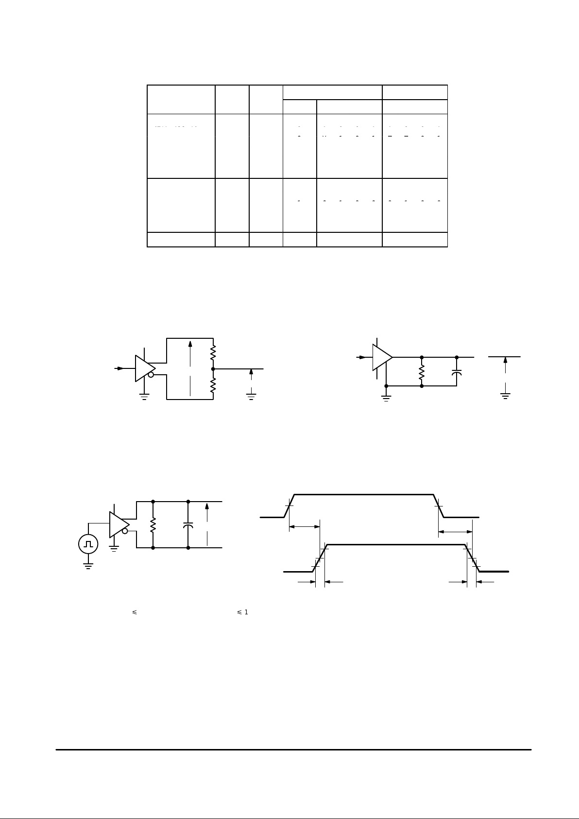
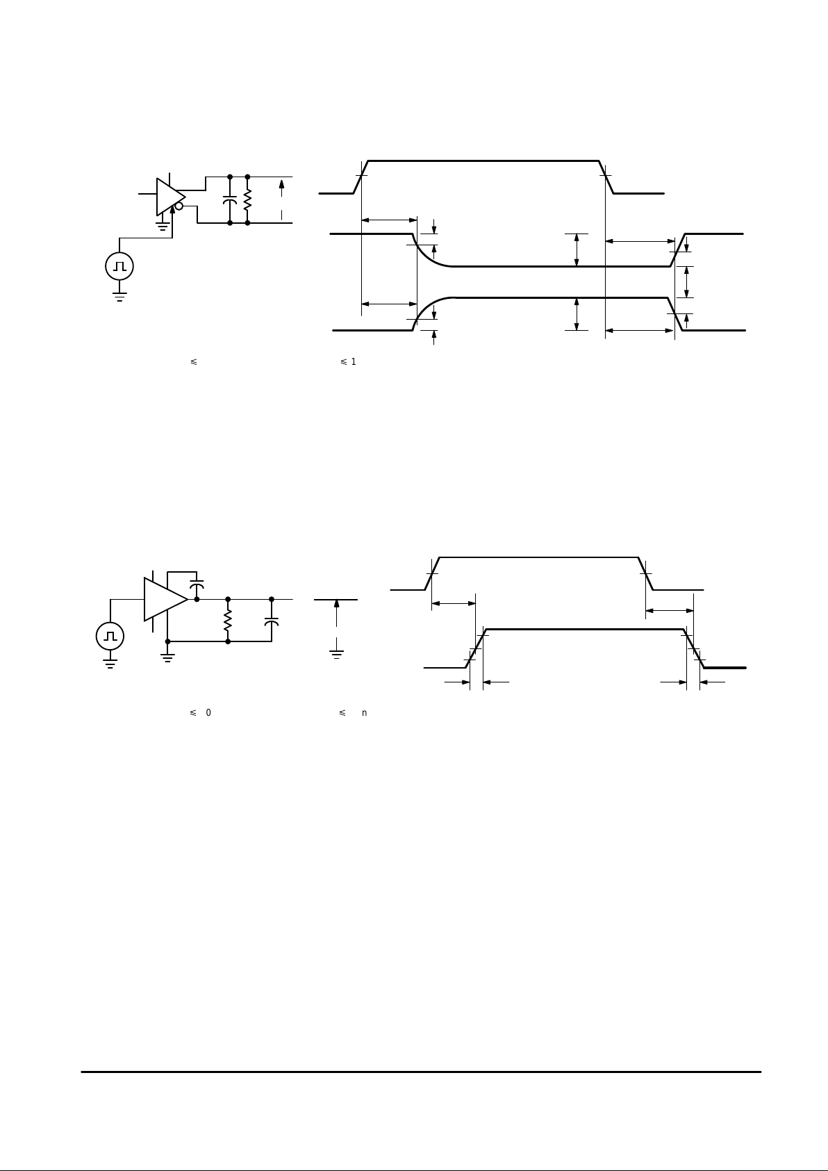
Figure 1. Differential Output Test Figure 2. Single–Ended Output Test
V
EE
Mode = 0
V
OS
R
L
RL/2
RL/2
C
L
V
in
(0.8 or 2.0 V)
V
CC
V
O
V
CC
V
OD2
Mode = 1
V
in
(0.8 or 2.0 V)
Figure 3. Differential Mode Rise/Fall Time and Data Propagation Delay
NOTES: 1. S.G. set to: f p 1.0 MHz; duty cycle = 50%; tr, tf, p 10 ns.
2.t
SK1
= t
PDH–tPDL
for each driver.
3.t
SK2
computed by subtracting the shortest t
PDH
from the longest t
PDH
of the 2 drivers within a package.
4.t
SK3
computed by subtracting the shortest t
PDL
from the longest t
PDL
of the 2 drivers within a package.
10%
t
PDH
1.5 V
V
in
0 V
10%
50%
90%
t
f
t
PDL
t
r
90%
50%
V
out
1.5 V
+3.0 V
V
CC
V
in
S.G.
V
OD
500 pF
100
AM26LS30
5
MOTOROLA ANALOG IC DEVICE DATA
Figure 4. Differential Mode Enable Timing
NOTES: 1. S.G. set to: f p 1.0 MHz; duty cycle = 50%; tr, tf, p 10 ns.
2.Above tests conducted by monitoring output current levels.
Figure 5. Single–Ended Mode Rise/Fall Time and Data Propagation Delay
NOTES: 1. S.G. set to: f p 100 kHz; duty cycle = 50%; tr, tf, p10 ns.
2.t
SK4
= t
PDH–tPDL
for each driver.
3.t
SK5
computed by subtracting the shortest t
PDH
from the longest t
PDH
of the 4 drivers within a package.
4.t
SK6
computed by subtracting the shortest t
PDL
from the longest t
PDL
of the 4 drivers within a package.
V
EE
t
PZH
t
PZL
t
PLZ
t
PHZ
1.5 V
Output
Current
(Vin = Lo)
0.1 VSS/R
L
0.1 VSS/R
L
VSS/R
L
VSS/R
L
0.5 VSS/R
L
0.5 VSS/R
L
R
L
0 or 3.0 V
En
V
SS
500 pF
450
Ω
S.G.
V
CC
450
C
C
+3.0 V
1.5 V
0 V
V
in
V
CC
V
in
+2.5 V
S.G.
500 pF
V
O
(Vin = Hi)
Vin
1.5 V
V
out
10%
50%
90%
t
r
1.5 V
90%
0 V
10%
V
in
50%
t
f
t
PDL
t
PDH
 Loading...