

MC26C32MOTOROLA
1
Product Preview
CMOS
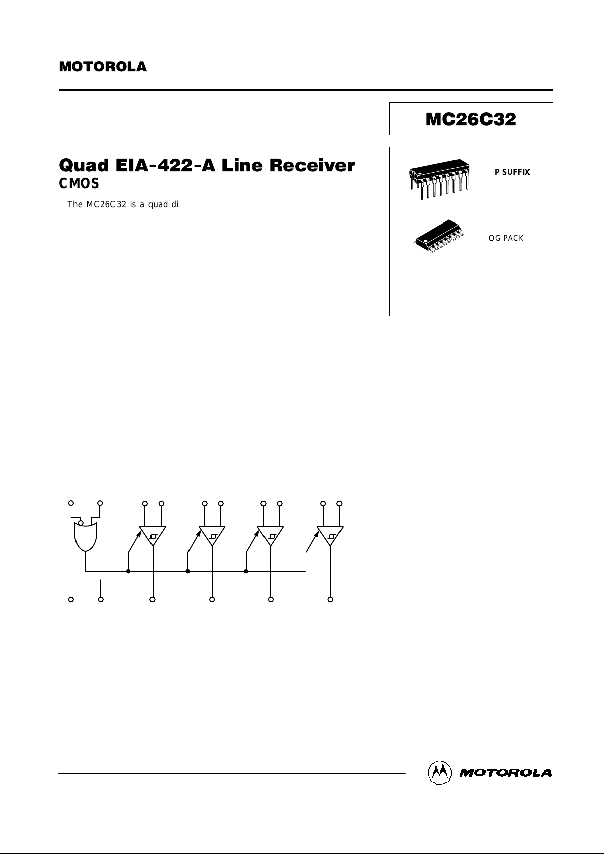
The MC26C32 is a quad differential line receiver designed for digital data
transmission over balanced lines. The MC26C32 meets all the requirements of
standard EIA–422–A while retaining the low–power characteristics of CMOS.
The MC26C32 has an input sensitivity of 200 mV over the common mode
input voltage range of ± 7 V. In addition, each receiver chain has internal
hysteresis circuitry to improve noise margin and discourage output instability for
slowly changing input waveforms.
The MC26C32 is pin compatible with the AM26LS32.
All pins are protected against damage due to electrostatic discharges.
• Typical Power Supply Current: 6 mA
• 2000 V ESD Protection on the Inputs and Outputs
• Typical Propagation Delay: 18 ns
• Typical Input Hysteresis: 75 mV
• Meets the Requirements of Standard EIA–422–A
• Operation from Single 5 V Supply
• High Impedance Mode for Outputs Connected to System Buses
• TTL/CMOS Compatible Outputs
BLOCK DIAGRAM
ENBENB
INPUT
D2
INPUT
C2
INPUT
B2
INPUT
A2
OUTPUT
D
OUTPUT
C
OUTPUT
B
OUTPUT
A
V
CC
GND
12 4
10 6 14 2
8 16 11 135 3
+ – + – + – + –
INPUT
D1
9
7 15 1
INPUT
C1
INPUT
B1
INPUT
A1
This document contains information on a product under development. Motorola reserves the right to change or discontinue this product without notice.
Order this document
by MC26C32/D
SEMICONDUCTOR TECHNICAL DATA
P SUFFIX
PLASTIC DIP
CASE 648
D SUFFIX
SOG PACKAGE
CASE 751B
ORDERING INFORMATION
MC26C32P Plastic DIP
MC26C32D SOG Package
16
1
16
1
Motorola, Inc. 1995
REV 4
10/95
MC26C32 MOTOROLA
2
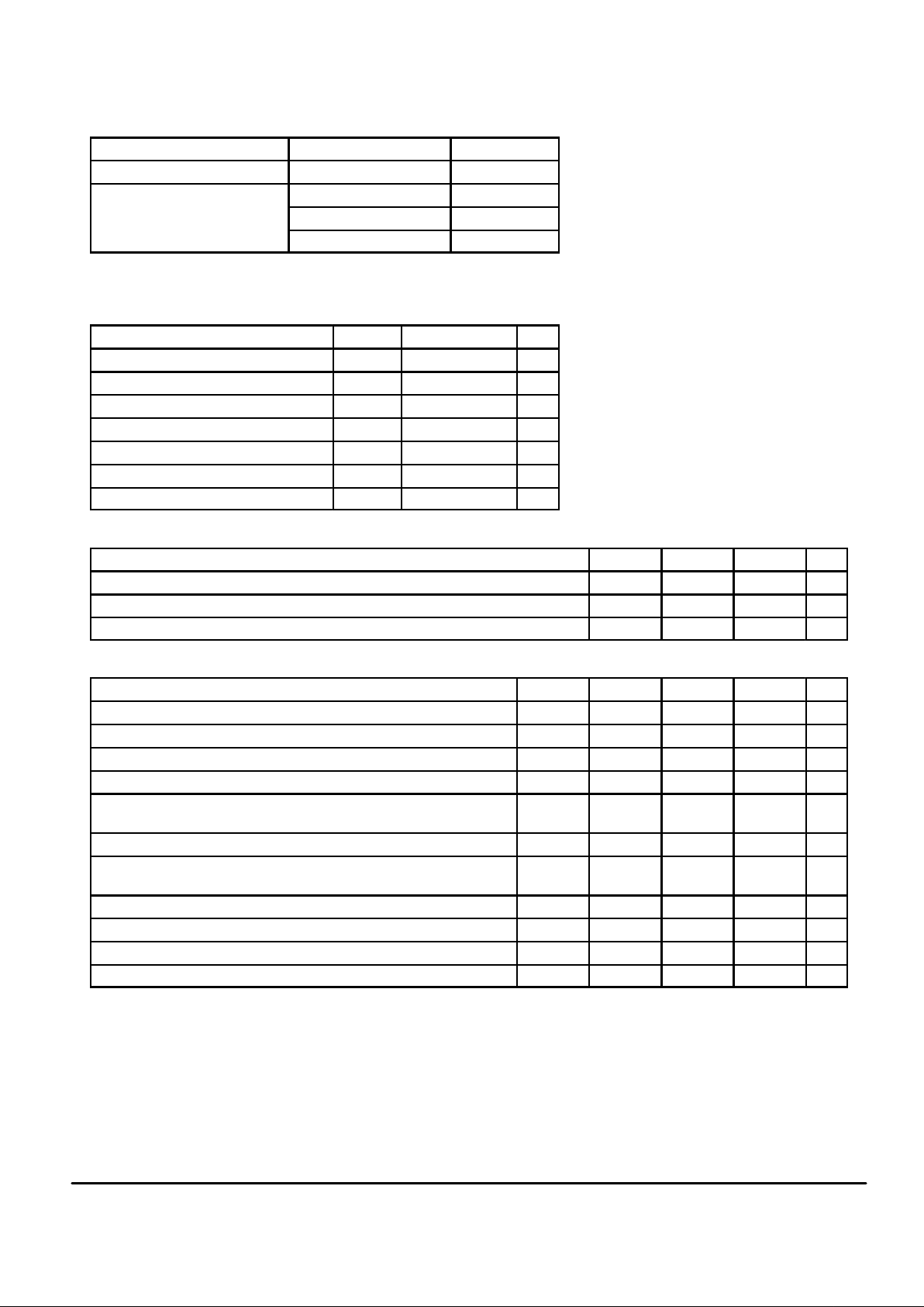
TRUTH TABLE
Control Inputs E/E Input Output
L/H X Z
All other combinations of
VID ≥ VTH (max) 1
enable inputs
VID ≥ VTH (min) 0
Open 1
X = Don’t Care H = High Logic State
Z = High Impedance L = Low Logic State
MAXIMUM RATINGS
Rating Symbol Value Unit
Power Supply Voltage V
CC
7 V
Input Voltage V
I
± 10 V
Input Differential Voltage V
ID
± 14 V
Enable Control Input Voltage V
in
VCC + 0.5 V
Storage Temperature T
stg
– 65 to + 150 °C
Maximum Current per Output I
O
± 25 mA
ESD (Human Body Model) 2000 V
OPERATING CONDITIONS
Rating Symbol Min Max Unit
Power Supply Voltage V
CC
4.5 5.5 V
Operating Temperature Range T
A
– 40 + 85 °C
Input Rise and Fall Time tr, t
f
— 500 ns
DC CHARACTERISTICS (V
CC
= 4.5 to 5.5 V, TA = – 40 to + 85°C, unless otherwise stated) (See Note 1)
Parameter
Symbol Min Typ Max Unit
Power Supply Current, VCC ≥ Max I
CC
— 6 12 mA
Enable Input Current, Vin = VCC or GND L
I
— — ± 1.0 µA
Input Voltage — Low Logic State (Enable Control) V
IL
— — 0.8 V
Input Voltage — High Logic State (Enable Control) V
IH
2 — — V
Differential Input Voltage, – 7 V < V
LCM
< 7 V V
out
= V
OH
V
out
= V
OL
V
TH
0.2
—
—
—
—
– 0.2
V
Input Hysteresis, V
LCM
= 0 V V
hys
— 75 — mV
Comparator Input Current Vin = + 10 V, Other Input = GND
Vin = – 10 V, Other Input = GND
I
in
—
—
1.4
– 2.5
—
—
mA
Comparator Input Resistance, – 10 V < V
LCM
< + 10 V R
in
4 4.8 — kΩ
Output Voltage (Low Logic State) VID = – 1 V, I
out
= 6 mA (Note 2) V
OL
— 0.13 0.33 V
Output Voltage (High Logic State) VID = + 1 V, I
out
= – 6 mA (Note 2) V
OH
3.8 4.8 — V
Output Leakage Current (High Logic State) V
out
= VCC or GND I
OZ
– 5 — 5 µA
NOTES:
1. All currents into device pins are shown as positive, out of device pins are negative. All voltages referenced to ground unless otherwise noted.
2. See EIA specifications EIA–422–A for exact test conditions.
This device contains circuitry to protect the
inputs against damage due to high static voltages or electric fields; however, it is advised that
normal precautions be taken to avoid applications of any voltage higher than the maximum
rated voltages to this high impedance circuit.
For proper operation it is recommended that
Vin and V
out
be constrained to the range VSS ≤
(Vin or V
out
) ≤ VDD. Reliability of operation is
enhanced if unused inputs are tied to and
appropriate logic voltage level (e.g., either V
SS
or VDD).
 Loading...