

Motorola MC1458D Datasheet
Order this document by MC1458/D
The MC1458, C was designed for use as a summing amplifier, integrator,
or amplifier with operating characteristics as a function of the external
feedback components.
• No Frequency Compensation Required
• Short Circuit Protection
• Wide Common Mode and Differential V oltage Ranges
• Low Power Consumption
• No Latch–Up
MAXIMUM RATINGS
Power Supply Voltage V
Input Differential Voltage V
Input Common Mode Voltage (Note 1) V
Output Short Circuit Duration (Note 2) t
Operating Ambient Temperature Range T
Storage Temperature Range T
Junction Temperature T
NOTES: 1.For supply voltages less than ±15 V, the absolute maximum
input voltage is equal to the supply voltage.
2.Supply voltage equal to or less than 15 V.
(TA = +25°C, unless otherwise noted.)
Rating Symbol Value Unit
V
CC
EE
ID
ICM
SC
A
stg
J
+18
–18
±30 V
±15 V
Continuous
0 to +70 °C
–55 to +125 °C
150 °C
Vdc
DUAL
OPERATIONAL AMPLIFIERS
(DUAL MC1741)
SEMICONDUCTOR
TECHNICAL DATA
8
1
P1 SUFFIX
PLASTIC PACKAGE
CASE 626
8
1
D SUFFIX
PLASTIC PACKAGE
CASE 751
(SO–8)
PIN CONNECTIONS
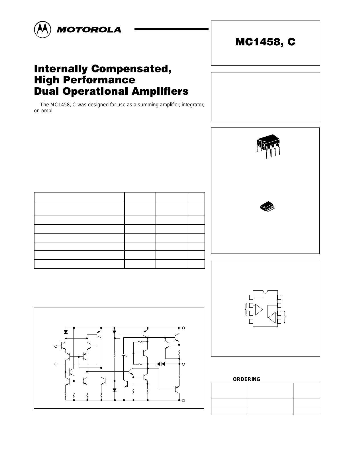
Representative Schematic Diagram
Noninverting
Input
Inverting
Input
1.0 k 1.0 k50 k
39 k
30 pF
MOTOROLA ANALOG IC DEVICE DATA
4.5 k
7.5 k
50 k 50
V
25
50
V
CC
Output
EE
Output A
Inputs
A
V
EE
1
2
–
+
3
4
(Top View)
A
8
V
CC
7
Output B
6
B
–
Inputs
+
5
B
ORDERING INFORMATION
Operating
Device
MC1458CD, D
MC1458CP1, P1
Motorola, Inc. 1996 Rev 1
Temperature Range
TA = 0° to +70°C
Package
SO–8
Plastic DIP
1
MC1458, C
ELECTRICAL CHARACTERISTICS
Characteristic Symbol
Input Offset Voltage (RS ≤ 10 k) V
Input Offset Current I
Input Bias Current I
Input Resistance r
Input Capacitance C
Offset Voltage Adjustment Range V
Common Mode Input Voltage Range V
Large Signal Voltage Gain A
(VO = ±10 V, RL = 2.0 k) 20 200 – – – –
(VO = ±10 V, RL = 10 k) – – – 20 200 –
Output Resistance r
Common Mode Rejection (RS ≤ 10 k) CMR 70 90 – 60 90 – dB
Supply Voltage Rejection (RS ≤ 10 k) PSR – 30 150 – 30 – µV/V
Output Voltage Swing V
(RS ≤ 10 k) ±12 ±14 – ±11 ±14 –
(RS ≤ 2.0 k) ±10 ±13 – ±9.0 ±13 –
Output Short Circuit Current I
Supply Currents (Both Amplifiers) I
Power Consumption P
Transient Response (Unity Gain)
(VI = 20 mV, RL ≥ 2.0 kΩ, CL ≤ 100 pF) Rise Time t
(VI = 20 mV, RL ≥ 2.0 kΩ, CL ≤ 100 pF) Overshoot os – 15 – – 15 – %
(VI = 10 V, RL ≥ 2.0 kΩ, CL ≤ 100 pF) Slew Rate SR – 0.5 – – 0.5 – V/µs
(VCC = +15 V, VEE = –15 V, TA = 25°C, unless otherwise noted. (Note 3))
MC1458 MC1458C
Min Typ Max Min Typ Max
IO
IO
IB
i
i
IOR
ICR
VOL
o
O
SC
D
C
TLH
– 2.0 6.0 – 2.0 1.0 mV
– 20 200 – 20 300 nA
– 80 500 – 80 700 nA
0.3 2.0 – – 2.0 – MΩ
– 1.4 – – 1.4 – pF
– ±15 – – ±15 – mV
±12 ±13 – ±11 ±13 – V
– 75 – – 75 – Ω
– 20 – – 20 – mA
– 2.3 5.6 – 2.3 8.0 mA
– 70 170 – 70 240 mW
– 0.3 – – 0.3 – µs
Unit
V/mV
V
ELECTRICAL CHARACTERISTICS (V
Characteristic Symbol
Input Offset Voltage (RS ≤ 10 kΩ) V
Input Offset Current (TA = 0° to +70°C) I
Input Bias Current (TA = 0° to +70°C) I
Output Voltage Swing V
(Rs ≤ 10 k) ±12 ±14 – – – –
(Rs ≤ 2 k) ±10 ±13 – ±9.0 ±13 –
Large Signal Voltage Gain A
(VO = ±10 V, RL = 2 k) 15 – – – – –
(VO = ±10 V, RL = 10 k) – – – 15 – –
*T
= 0°C for MC1458, C T
low
NOTE: 3. Input pins of an unused amplifier must be grounded for split supply operation or biased at least 3.0 V above VEE for single supply operation.
= +70°C for MC1458, C
high
= +15 V, VEE = –15 V, TA = T
CC
IO
IO
IB
O
VOL
to T
high
MC1458 MC1458C
Min Typ Max Min Typ Max
– – 7.5 – – 12 mV
– – 300 – – 400 nA
– – 800 – – 1000 nA
, unless otherwise noted. (Note 3))*
low
Unit
V
V/mV
2
MOTOROLA ANALOG IC DEVICE DATA
MC1458, C
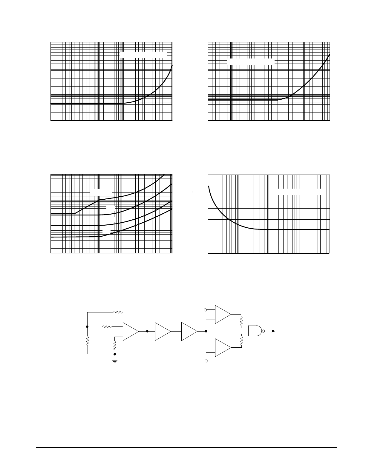
Figure 1. Burst Noise versus Source Resistance Figure 2. RMS Noise versus Source Resistance
1000
100
µ
100
10
,INPUT NOISE (peak) ( V)
n
e
0
10 100 1.0 k 10 k 100 k 1.0 M
RS, SOURCE RESISTANCE (Ω)
BW = 1.0 Hz to 1.0 kHz
µ
10
1.0
,INPUT NOISE (peak) ( V)
n
e
0.1
10 100 1.0 10 k 100 k
BW = 1.0 Hz to 1.0 kHz
RS, SOURCE RESISTANCE (Ω)
Figure 3. Output Noise versus Source Resistance Figure 4. Spectral Noise Density
10
1.0
0.1
OUTPUT NOISE (rms mV)
,
n
e
AV = 1000
100
10
1.0
140
120
)
Hz
100
√
nV/
80
60
40
INPUT NOISE (
,
n
e
20
AV = 10, RS = 100 k
1.0 M
Ω
0
10 100 1.0 k 10 k 100 k 1.0 M
RS, SOURCE RESISTANCE (Ω)
Figure 5. Burst Noise Test Circuit
100 k
100 k
1.0 k
Unlike conventional peak reading or RMS meters, this system
was especially designed to provide the quick response time
essential to burst (popcorn) noise testing.
100 k
–
+
Operational Amplifier
Under Test
X 500 X 2
Positive
Threshold
Voltage
Low Pass Filter
1.0 Hz to 1.0 kHz
Negative
Threshold
Voltage
The test time employed is 10 sec and the 20 µV peak limit
refers to the operational amplifier input thus eliminating errors
in the closed loop gain factor of the operational amplifier .
0
10 100 1.0 k 100 k10 k
f, FREQUENCY (Hz)
+
–
To Pass / Fail
Indicator
–
+
MOTOROLA ANALOG IC DEVICE DATA
3
 Loading...