

Motorola MC145426DW, MC145426P, MC145422DW, MC145422P Datasheet
SEMICONDUCTOR TECHNICAL DATA
Order this document
by MC145422/D
The MC145422 and MC145426 UDLTs are high–speed data transceivers
that provide 80 kbps full–duplex data communication over 26 AWG and larger
twisted–pair cable up to two kilometers in distance. Intended primarily for use in
digital subscriber voice/data telephone systems, these devices can also be
used in remote data acquisition and control systems. These devices utilize a
256 kilobaud modified differential phase shift keying burst modulation technique
for transmission to minimize RFI/
distribution and duplex data communication can be obtained using a single
twisted–pair wire.
These devices are designed for compatibility with existing, as well as
evolving, telephone switching hardware and software architectures.
The UDLT chip–set consists of the MC145422 Master UDLT for use at the
telephone switch linecard and the MC145426 Slave UDL T for use at the remote
digital telset and/or data terminal.
The devices employ CMOS technology in order to take advantage of their
reliable low–power operation and proven capability for complex analog/digital
LSI functions.
• Provides Full–Duplex Synchronous 64 kpbs Voice/Data Channel and Two
8 kbps Signaling Data Channels Over One 26 AWG Wire Pair Up to Two
Kilometers
• Compatible with Existing and Evolving Telephone Switch Architectures and
Call Signaling Schemes
• Automatic Detection Threshold Adjustment for Optimum Performance Over
V arying Signal Attenuations
• Protocol Independent
• Single 5 V Power Supply
• 22–Pin PDIP, 24–Pin SOG Packages
• Application Notes AN943, AN949, AN968, AN946, and AN948
MC145422 Master UDL T
• Pin Controlled Power–Down and Loopback Features
• Signaling and Control I/O Capable of Sharing Common Bus Wiring with
Other UDLTs
• V ariable Data Clock — 64 kHz to 2.56 MHz
• Pin Controlled Insertion/Extraction of 8 kbps Channel into LSB of 64 kbps
Channel for Simultaneous Routing of Voice and Data Through PCM Voice
Path of Telephone Switch
MC145426 Slave UDL T
• Compatible with MC145500 Series PCM Codec–Filters
• Pin Controlled Loopback Feature
• Automatic Power–Up/Power–Down Feature
• On–Chip Data Clock Recovery and Generation
• Pin Controlled 500 Hz D3 or CCITT Format PCM Tone Generator for
Audible Feedback Applications
EMI and crosstalk. Simultaneous power
P SUFFIX
22
1
24
1
ORDERING INFORMATION
MC145422P Plastic DIP
MC145426P Plastic DIP
MC145422DW SOG Package
MC145426DW SOG Package
PLASTIC DIP
CASE 708
DW SUFFIX
SOG PACKAGE
CASE 751E
REV 2
9/95
Motorola, Inc. 1995
MC145422•MC145426MOTOROLA
1
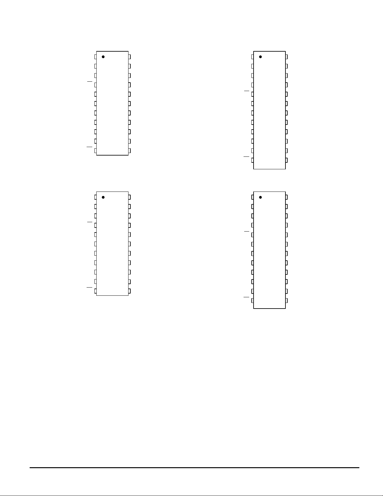
PIN ASSIGNMENTS
MC145422 — MASTER
(PLASTIC PACKAGE)
1
V
SS
V
ref
LI
LB
VD
SI1
SO1
SI2
SO2
SE
PD
2
3
4
5
6
7
8
9
10
11
22
21
20
19
18
17
16
15
14
13
12
V
DD
LO1
LO2
RE1
Rx
TDC/RDC
CCI
Tx
TE1
SIE
MSI
MC145426 — SLA VE
(PLASTIC PACKAGE)
1
V
SS
V
ref
LI
LB
VD
SI1
SO1
SI2
SO2
Mu/A
PD
2
3
4
5
6
7
8
9
10
11
22
21
20
19
18
17
16
15
14
13
12
V
DD
LO1
LO2
RE1
Rx
CLK
X2
X1
Tx
TE1
TE
NC = NO CONNECTION
MC145422 — MASTER
(SOG PACKAGE)
1
V
SS
2
V
ref
3
LI
4
NC NC
5
LB
VD
6
7
SI1
SO1
8
SI2
9
10
SO2
SE
11
PD
12
24
23
22
21
20
19
18
17
16
15
14
13
V
DD
LO1
LO2
RE1
Rx
TDC/RDC
CCI
Tx
TE1
SIE
MSI
MC145426 — SLA VE
(SOG PACKAGE)
1
V
SS
2
V
ref
3
LI
421NC NC
LB
5
VD
6
SI1
7
8
SO1
9
SI2
10
SO2
11
Mu/A
PD
12
24
23
22
20
19
18
17
16
15
14
13
V
DD
LO1
LO2
RE1
Rx
CLK
X2
X1
Tx
TE1
TE
MC145422•MC145426 MOTOROLA
2
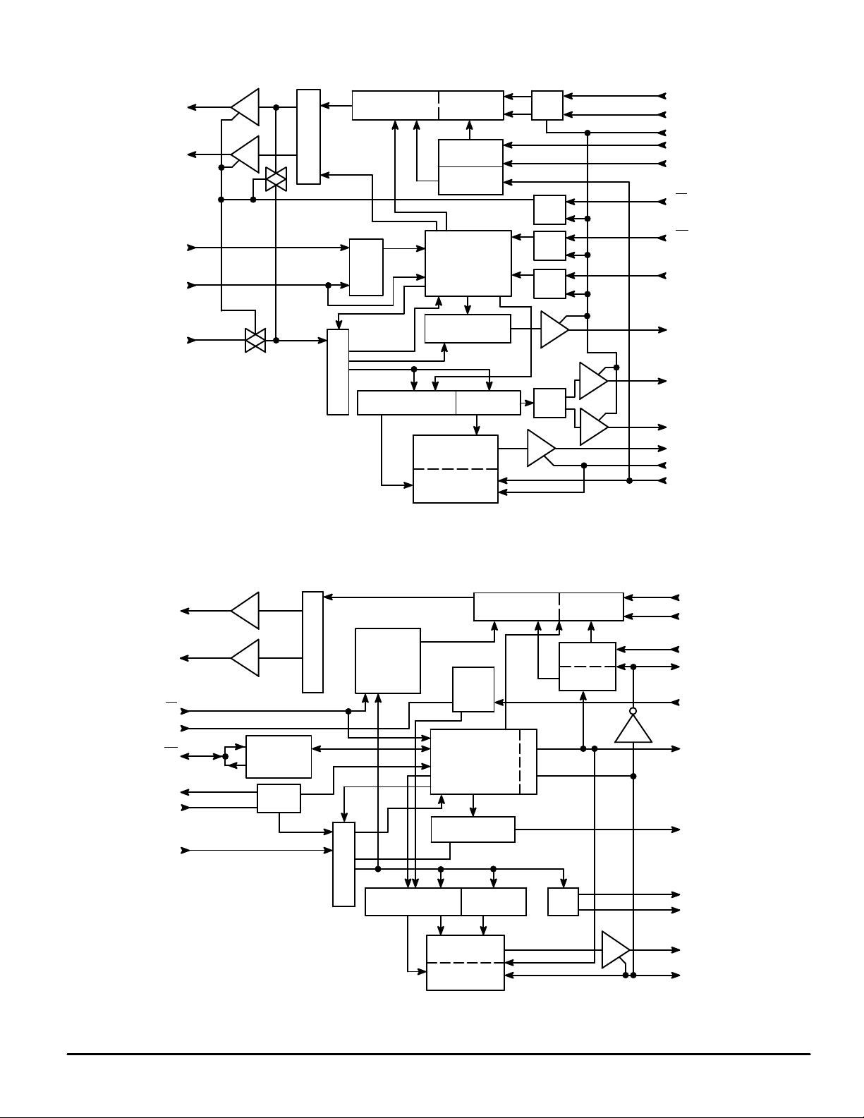
MC145422 MASTER UDLT BLOCK DIAGRAM
LO1
LO2
CCI
MSI
LI
*— SE controlled latch
+ 1
– 1
MODULA TION BUFFER
MODULATOR
RECEIVE
REGISTER
*
SI1
SI2
SE
RE1
Rx
LB
*
PD
SIE
DIVIDE
SEQUENCE
AND
CONTROL
*
*
VD CONTROL
DEMODULATOR
DEMODULA TION BUFFER
TRANSMIT
REGISTER
*
VD
SO1
SO2
Tx
TE1
TDC/RDC
LO1
LO2
LB
TE
PD
X2
X1
LI
+ 1
– 1
POWER–
DOWN
CONTROL
OSC
MC145426 SLAVE UDLT BLOCK DIAGRAM
MODULA TION BUFFER
LOOPBACK
MODULATOR
CONTROL
SEQUENCE
CONTROL
VD CONTROL
DEMODULATOR
DEMODULA TION BUFFER
TRANSMIT
TONE
GEN.
AND
RECEIVE
REGISTER
*
SI1
SI2
Rx
RE1
Mu/A
CLK
VD
SO1
SO2
Tx
REGISTER
TE1
MC145422•MC145426MOTOROLA
3
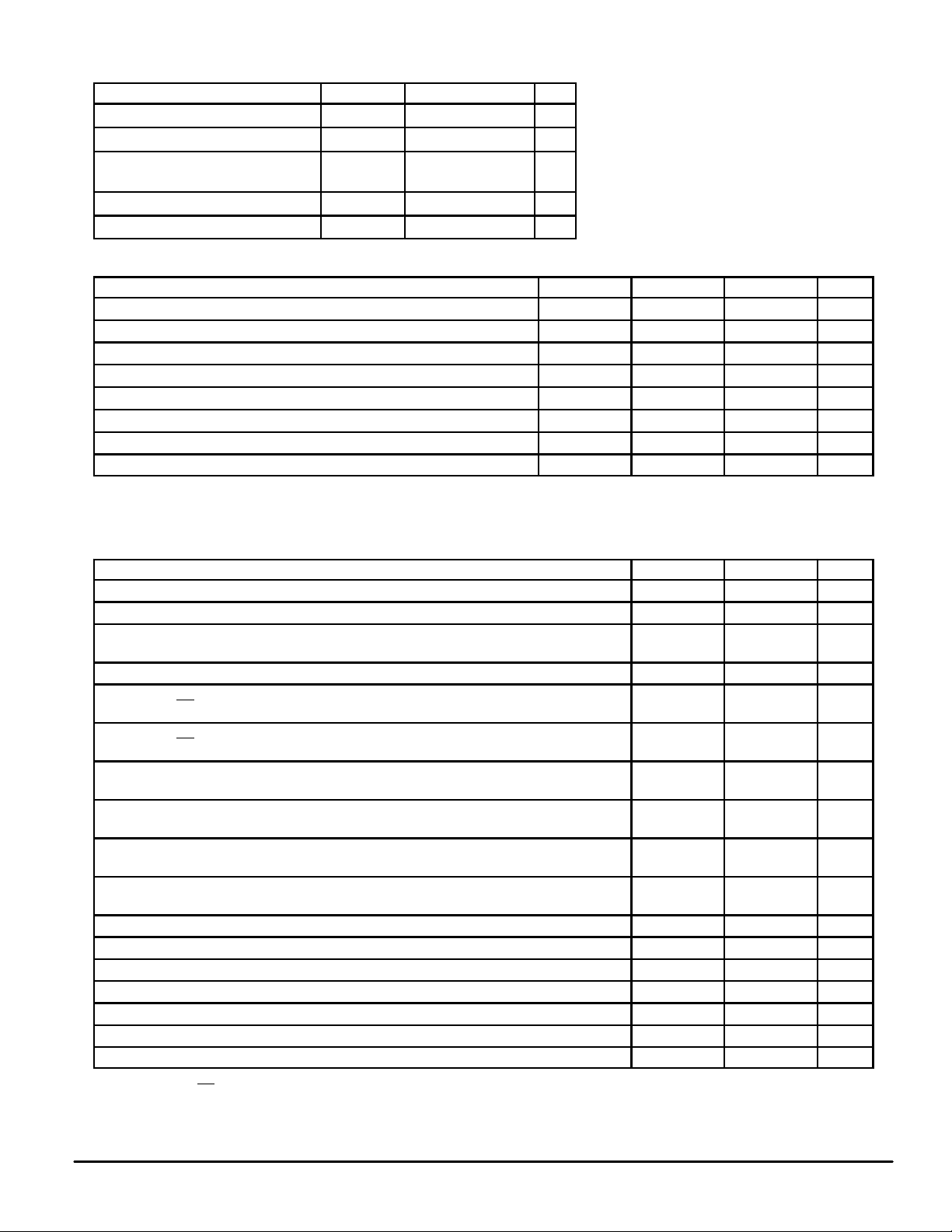
ABSOLUTE MAXIMUM RATINGS (Voltage Referenced to V
Rating
DC Supply Voltage VDD – V
Voltage, Any Pin to V
DC Current, Any Pin (Excluding VDD,
VSS)
Operating Temperature T
Storage Temperature T
SS
RECOMMENDED OPERATING CONDITIONS (T
Parameter
DC Supply Voltage V
Power Dissipation (PD = VDD, VDD = 5 V) V
Power Dissipation (PD = VSS, TE = VSS) V
MC145422 Frame Rate MSI 7.9 8.1 kHz
MC145422 — MC145426 Frame Rate Slip (See Note 1) — — 0.25 %
CCI Clock Frequency (MSI = 8 kHz) CCI — 2.048 MHz
Data Clock Rate MC145422 TDC, RDC 64 2560 kHz
Modulation Baud Rate (See Note 2) LO1, LO2 — 256 kHz
NOTES:
1. The MC145426 crystal frequency divided by 512 must equal the MC145422 MSI Frequency ± 0.25% for optimum operation.
2. Assumes crystal frequency of 4.096 MHz for the MC145426 and 2.048 MHz CCI for the MC145422.
Symbol Value Unit
SS
V – 0.5 to VDD + 0.5 V
I ± 10 mA
A
stg
= 0 to 70°C)
A
)
SS
– 0.5 to + 9.0 V
– 40 to + 85 °C
– 85 to + 150 °C
This device contains circuitry to protect the
inputs against damage due to high static
voltages or electric fields; however, it is
advised that normal precautions be taken to
avoid applications of any voltage higher than
maximum rated voltages to this high impedance circuit. For proper operation it is recommended that Vin and V
the range VSS ≤ (Vin or V
Reliability of operation is enhanced if unused
inputs are tied to an appropriate logic voltage
level (e.g., either VSS or VDD).
Pins Min Max Unit
DD
DD
DD
4.5 5.5 V
— 80 mW
— 75 mW
be constrained to
out
) ≤ VDD.
out
DIGITAL CHARACTERISTICS (V
Input High Level 3.5 — V
Input Low Level — 1.5 V
Input Current Except LI
Input Capacitance — 7.5 pF
Output High Current (Except Tx on MC145422 VOH = 2.5 V
and Tx and PD
Output Low Current (Except Tx on MC145422 VOL = 0.4 V
and Tx and PD
PD Output High Current (MC145426) (See Note 1) VOH = 2.5 V
PD Output Low Current (MC145426) (See Note 1) VOL = 0.4 V
Tx Output High Current VOH = 2.5 V
Tx Output Low Current VOL = 0.4 V
Tx Input Impedance (TE1 = VSS, MC145422) 100 — kΩ
Crystal Frequency (MC145426, Note 2) 4.0 4.4 MHz
PCM Tone (TE = VDD, MC145426) – 22 – 18 dBm0
Three–State Current (SO1, SO2, VD, Tx on MC145422, Tx on MC145426) — ± 1 µA
V
Voltage (See Note 3) 2 3 V
ref
X2 — Oscillator Output High Drive Current (MC145426) (See Note 4) VOH = 4.6 V – 450 — µA
X2 — Oscillator Output Low Drive Current (MC145426) (See Note 4) VOL = 0.4 V 450 — µA
NOTES:
1. To overdrive PD
2. The MC145426 crystal frequency divided by 512 must equal the MC145422 MSI frequency ± 0.25% for optimum performance.
3. V
ref
4. Output drive when X1 is being driven from an external clock.
on MC145426) VOH = 4.6 V
on MC145426) VOL = 0.8 V
from a low level to 3.5 V or a high level to 1.5 V requires a minimum of ± 800 µA drive capability.
typically (9/20 VDD – VSS).
= 5 V, TA = 0 to 70°C)
DD
Parameter
VOH = 4.6 V
VOL = 0.8 V
VOH = 4.6 V
VOL = 0.8 V
Min Max Unit
LI
– 1.0
– 100
– 1.7
– 0.36
0.36
0.8
– 90
– 10
60
100
– 3.4
– 0.7
1.7
3.5
1.0
100
—
—
—
—
—
—
—
—
—
—
—
—
mA
mA
mA
mA
µA
µA
µA
MC145422•MC145426 MOTOROLA
4
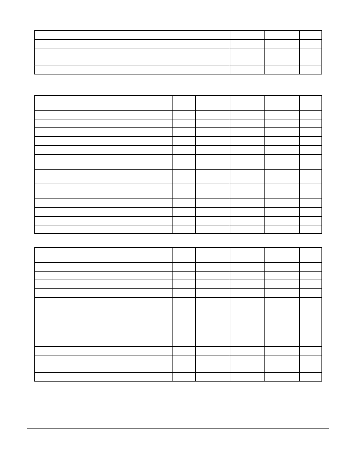
ANALOG CHARACTERISTICS (V
Modulation Differential Amplitude (RL = 440 Ω) LO1 to LO2 4.5 6.0 V p–p
Modulation Differential DC Offset 0 300 mV
Demodulator Input Amplitude (See Note) 0.050 2.5 V peak
Demodulator Input lmpedance 50 150 kΩ
NOTE: The input level into the demodulator to reliably demodulate incoming bursts. Input referenced to V
= 5 V, TA = 0 to 70°C)
DD
Parameter
Min Max Unit
.
ref
MC145422 SWITCHING CHARACTERISTICS (V
Parameter
Input Rise Time All Digital Inputs 1 t
Input Fall Time All Digital Inputs 1 t
Pulse Width TDC/RDC, RE1, MSI 1 tw(H,L) 90 — ns
CCI Duty Cycle 1 tw(H,L) 45 55 %
Data Clock Frequency TDC/RDC — t
Propagation Delay Time MSI to SO1, SO2 VD (PD = VDD)
MSI to TDC/RDC Setup Time 4 t
TE1/RE1 to TDC/RDC Setup Time 4 t
Rx to TDC/RDC Setup Time 5 t
Rx to TDC/RDC Hold Time 5 t
SI1, SI2 to MSI Setup Time 6 t
SI1, SI2 to MSI Hold Time 6 t
MC145426 SWITCHING CHARACTERISTICS (V
Parameter
Input Rise Time All Digital Inputs 1 t
Input Fall Time All Digital Inputs 1 t
Clock Output Pulse Width CLK 1 tw(H,L) 3.8 4.0 µs
Crystal Frequency — f
Propagation Delay Times TE1 Rising to CLK (TE = VDD)
TE1 Rising to CLK (TE = VSS)
CLK to TE1 Falling
CLK to RE1 Rising
RE1 Falling to CLK (TE = VDD)
RE1 Falling to CLK (TE = VSS)
TE1 to SO1, SO2
Rx to CLK Setup Time 5 t
Rx to CLK Hold Time 5 t
SI1, SI2 to TE1 Setup Time 6 t
SI1, SI2 to TE1 Hold Time 6 t
= 5 V, TA = 25°C, CL = 50 pF)
DD
Figure
No.
TDC to Tx
= 5 V, TA = 25°C, CL = 50 pF)
DD
CLK to Tx
2
3
Figure
No.
7
7
7
8
8
8
9
9
Symbol Min Max Unit
r
f
DC
t
, t
PLH
PHL
su3
t
su4
su3
t
su4
su5
h1
su6
h2
Symbol Min Max Unit
r
f
X1
t
p1
t
p1
t
p2
t
p3
t
p4
t
p4
t
p5
t
p6
su5
h1
su6
h2
— 4 µs
— 4 µs
64 2560 kHz
—
—
90
40
90
40
60 — ns
60 — ns
60 — ns
60 — ns
— 4 µs
— 4 µs
4.086 4.1 MHz
– 50
438
—
—
– 50
438
—
—
60 — ns
60 — ns
60 — ns
60 — ns
90
90
—
—
—
—
50
538
40
40
50
538
90
90
ns
ns
ns
ns
MC145422•MC145426MOTOROLA
5
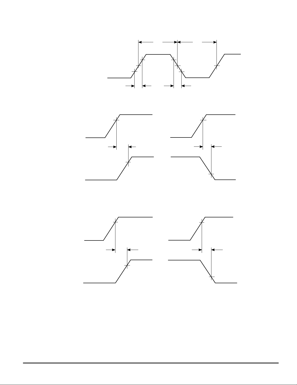
SWITCHING WAVEFORMS
CLK, TDC, RDC, RE1, CCI, MSI
MSI
VD, SO1, SO2
10%
t
w(H)
90%
50%
t
r
t
f
t
w(L)
Figure 1.
70% 70%
t
PHL
70%
t
PLH
50%
30%
TDC
Tx
Figure 2.
70% 70%
t
PLH
70%
t
PHL
Figure 3.
30%
MC145422•MC145426 MOTOROLA
6
 Loading...