

Motorola MC145192EVK, MC145202EVK Datasheet

MC145192EVK • MC145202EVK
1
MOTOROLA
INTRODUCTION
The MC145192EVK and MC145202EVK are two versions of one board with a few component changes.
They allow users to exercise features of both devices and to build PLLs which meet individual performance requirements. The control program works with any board and can be used with other Motorola
PLL devices (MC145190, MC145191, MC145200, MC145201, MC145220*). It will select frequency defaults that apply to each. All board functions are controlled through the printer port of an IBM PC. Up to
three different EVKs may be controlled at the same time from one printer port. The functional block diagram is given in Figure 1.
This manual is divided into two sections. Section 1 describes the hardware and Section 2 covers the
software control program.
VCO
733–751 MHz
MC145192
MC145202
PLL
Control Voltage
External Reference Input
TCXO Reference
RF Output
Frequency
Control Data
Out A, Out B
Lock Detect
Loop Filter
2nd Harmonic
Filter, Amplifier
74HCT241, 74LS126
Buffer Logic
Logic Control Switches
Parallel Port Connector
Isolation Resistor
PD
out
Current
F
in
Figure 1. Evaluation Kit Block Diagram
* The MC145220 is not available with Rev. 2.5 software.
All brand names and product names appearing in this document are registered trademarks or trademarks of their respective holders.
SEMICONDUCTOR TECHNICAL DATA
Motorola, Inc. 1996
REV 1
3/96

MC145192EVK • MC145202EVK
MOTOROLA
2
SECTION 1 – HARDWARE
FEATURES
1. The EVK is a complete working synthesizer, including VCO.
2. Control program is written in Turbo Pascal.
3. Board is controlled by an IBM PC–compatible computer through the printer port.
4. Up to three boards can be operated independently through one printer port.
5. A prototype area and mounting holes are provided for VCOs, mixers, and amplifiers.
6. External reference input can be used.
7. Five element loop filter is included.
8. Frequency range of operation, step size and reference frequency can be changed in the control
program.
9. Lock Detect, Out A, and Out B on any single board are accessible through the printer port.
CONTENTS OF EVALUATION KIT
1. Assembled evaluation board.
2. Nine–foot flat cable with four DB–25 male connectors.
3. MC145192/202 EVK manual.
4. 3.5″ PC–compatible disk containing compiled program.
5. PLL device data sheets.
GETTING STARTED
To perform basic functions, do the following:
1. Plug in 12 volts at J6, observing the polarity marked on the board.
2. Short circuit section 1 of the DIP switch (S1) and open circuit all other sections.
3. Connect the supplied flat cable between the computer printer port and the DB–25 connector on
the board (J5).
4. Type PLL at the DOS prompt. Then press enter.
5. Type the number that corresponds with the type of board given in the on–screen menu. Then
press Q.
You should now see the main menu displayed. There should be a signal present at J8 on the current
output frequency given in the main menu. If the signal is not on the correct frequency , check to see if your
printer card address is $278 (hexadecimal 278). If not, then select the P menu item and enter the correct
address. After returning to the main menu, select the I menu item to send data to the board. You should
now be on frequency.
MODIFICATIONS
The user may modify the hardware, such as utilizing a different VCO, by using the prototyping area of the
board. After such modifications are made, the default values in the software may need to be changed.
This is facilitated from screen #2 ‘Select from the available options’ screen.
Note that the on–board voltage regulators allow for maximum control voltage range of 0.5 to 4.5 V.

MC145192EVK • MC145202EVK
3
MOTOROLA
TYPICAL PERFORMANCE
Common to both kits, unless noted. Typical performance applies only to the configuration as shipped.
The MC145192EVK is shipped with VCC = 3 V and VPD = 5 V. The MC145202EVK is shipped with
VCC = 5 V and VPD = 5 V.
Supply Voltage (J6) 11.5 – 12.5 V
Supply Current (J6) (Note 1) 120 mA
Available Current (Note 2)
60 mA
Frequency Range (’192) (Note 3) 733 – 743 MHz
Frequency Range (’202) (Note 3) 1466 – 1486 MHz
Reference Frequency 14.4 MHz
Temperature Stability (– 30°C to + 85°C) < ± 2 ppm
TCXO Aging < ± 1 ppm / year
Step Size (’192) 100 kHz
Step Size (’202) 200 kHz
Power Output 4.5 – 7.5 dBm
2nd Harmonic Level (’192) < – 18 dB
Fundamental Level (’202) < – 23 dB
3rd Harmonic Level < – 18 dB
Frequency Accuracy (’192) ± 1.5 kHz
Frequency Accuracy (’202) ± 3.0 kHz
Reference Sidebands – 70 dB
Phase Noise (100 Hz, ’192) – 70 dBc/Hz
Phase Noise (100 Hz, ’202) – 69 dBc/Hz
Phase Noise (10 kHz, ’192) (Note 4) – 86 dBc/Hz
Phase Noise (10 kHz, ’202) (Note 4) – 90 dBc/Hz
Switching Time (Note 5) 2.6 ms
NOTES:
1. Supply current is current the board requires without user modifications.
2. Available current is the sum of currents available to the user (in the prototype area) from the 5 V and 8.5 V supply. The 12 V supply is not
regulated. Current at 12 V is limited by the external power supply . If the on–board VCO and amplifier are disconnected from the power bus,
more current can be drawn in the prototype area. The current flowing into U3 (the 8.5 V regulator) should not exceed 180 mA. This will limit
temperature rise in U3.
3. Frequency ranges require use of the 5 V default charge pump supply voltage.
4. 10 kHz phase noise is limited by the PLL device noise. For low noise designs, the loop bandwidth is made more narrow and the VCO is relied
upon to provide the 10 kHz phase noise. This can be seen on the EVKs since the VCO has much lower noise.
5. 10 MHz step, within ± 1 kHz of final frequency (’192).
20 MHz step, within ± 2 kHz of final frequency (’202).

MC145192EVK • MC145202EVK
MOTOROLA
4
SUPPORT MATERIAL
To provide further information, the following documents are included:
1. Schematic diagram of ’192/202EVK.
2. Separate Bill of Materials for each board.
3. Parts layout diagram.
4. Mechanical drawing of board.
5. MC145192 and MC145202 data sheets.
6. Printer port diagram.
7. Typical signal plots for each type of EVK.
PRODUCTION TEST
After assembly is complete, the following alignment and test is performed on ’192EVK (or ’202EVK):
1. The control program is started in single board ’190EVK (’200EVK) mode.
2. L menu item is selected.
3. Power is applied to the board. DIP switch section 1 is closed circuit with all others being open
circuit.
4. After attaching computer cable, menu item I is selected.
5. Trim resistor VR1 is adjusted to obtain an output frequency at J8 of 740.999 – 741.001 MHz
(1481.998 – 1482.002 MHz).
6. Voltage at the control voltage test point is measured. It must be 2.5 – 3.1 V.
7. When testing more than 1 board, steps 3 – 6 are repeated.
If in step 5 it isn’t possible to obtain a signal on frequency, menu item P should be selected and the correct printer port address entered. Menu item I would then be selected to reload the data.
BOARD OPERATION
A computer is connected to the DB–25 connector J5. Data is output from the printer port. The printer card
is in slot 0 using the default address in the control program. Data is sent to the PLL device (U1) through
the DIP switch (S1), and 74HCT241 buffer (U5). D2, D3, D4, R19, R20, and R21 are in the data path
between the 74HCT241 and PLL devices. This limits the high level output voltage of the buffer. Voltage
on the PLL device inputs must not be greater than 0.5 V above VCC. A ’192/202 PLL has three output
lines which are routed through a 74LS126 line driver (U2) to the computer.
U5, the 74HCT241, provides isolation, logic translation and a turn–on delay for PLL input lines. Logic
translation is needed from the TTL levels on the printer port to the CMOS levels on the ’192/202 inputs.
Turn–on delay is used to ensure the power–on reset functions properly. The enable line to the PLL must
be held low during power–up.
A 12 V power supply should be used to power the board at J6 (Augat 2SV–02 connector). The 2SV–02
will accept 18–24 AWG bare copper power leads. No tools are needed for connection. If power is properly connected, LED D2 will be lit.
Power passes from J6 to U3 (LM317 regulator) configured as an 8.5 V regulator. Both boards use 8.5 V
to power the VCO and RF amplifier. Regulators U4 and U7 use the 8.5 V supply to produce 3 V and 5 V.
The ’192 always uses 3 V to power logic and 5 V to power the charge pump, while the ’202 can have
either power both the logic and charge pump. J3 and J4 are jumpers which select voltages for the logic
and charge pump supplies. U4 and U7 are cascaded with U3 to equalize their individual voltage drops.
The PLL loop is composed of the PLL device (U1), 733 – 743 MHz VCO (M1), passive loop filter (R11,
R12, C4, C5, C6) and second harmonic filter amplifier (U6). A passive loop filter was used to keep the

MC145192EVK • MC145202EVK
5
MOTOROLA
design simple, reduce noise, and reduce the quantity of traces susceptible to stray pickup. About 56 dB
rejection of fundamental and 23 dB gain is provided by the harmonic filter amplifier. This allows the ’202
to lock at 1466 – 1486 MHz.
A single VCO model is used for both boards. It is an internal Motorola part which is not sold for other
applications. The ’192 operates at half the output frequency and step size of the ’202. This allows the
same loop filter components to be used. RF is fed to the PLL chip Fin input through voltage dividers R14
and R10. These two resistors terminate the PLL chip RF input with 50 ohms and provide isolation.
Both boards use a phase detector current of 2 mA. J1 and J2 are removable jumpers and cut traces.
They are used as connection points for a current measurement of VPD or VCC. A potentiometer VR1 is
used to set M2 (14.4 MHz TCXO) on frequency.
COMPONENTS UNIQUE TO EACH EVK
Components that are not the same on all EVKs are given in the following table:
’192EVK
’202EVK
U1
MC145192
MC145202
R2
18 kΩ
3.9 kΩ
R8
0 Ω
Not Used
C22
Not Used
1.0 pF
J3
3 V
5 V
EXTERNAL REFERENCE INPUT
As shipped, all boards are configured for a 14.4 MHz TCXO (supplied). To use an external reference,
disconnect J13 and connect J9. Use a reference signal at J10 which complies with data sheet requirements. Then modify the reference frequency in the program main menu to reflect the changes made ( [F]
menu item ).
DATA TRANSFER FROM COMPUTER TO EVK
To control the serial input EVK with the parallel printer port, a conversion is done. Printer cards are designed to output eight bits through eight lines. A bit mask is used to obtain the bit combination for the
three required output lines (Data, Clock, Load). As bytes are sent to the printer card in sequence, it appears to be a serial transfer. The printer port is used because data transfer using the serial port is much
slower. A standard IBM PC can support a parallel port data rate of 4.77 MHz.
IBM PCs and compatibles can accept up to three printer port cards. These ports are called LPT1, LPT2,
and LPT3. Each printer card has jumpers or DIP switches on it to set a unique address. Two sets of
addresses are in common use. One set applies to IBM PC XT, AT, and clones. The other is for the PS 2
line. To load data into the EVK, the correct address must be selected. The program default is $278, which
is LPT1 in a clone. If $278 is not the address in use, it must be modified by entering the O menu item in
the main menu. All allowed addresses given in hexadecimal are as follows:
Label
IBM PC and Clones PS 2
LPT1 278 3BC
LPT2 378 378
LPT3 3BC 278
MC145192EVK • MC145202EVK
MOTOROLA
6
Up to three EVK boards can operate independently from one printer port. All lines on the printer port are
connected to every EVK. Even with three boards operating, only three output lines (Clock, Data and
Load) from the printer card are used. If two boards are controlled together, data for the second board is
received from the Output A of the first. Output A is a configurable output on ’192/202 devices, which in
this case is used to shift data through chip 1 into chip 2. Output A and Data are connected using a printer
port input line. This was done to avoid connecting extra wires. Fortunately not all port input lines are
needed for computer input. Load and Clock are common to both boards.
A three–board cascade is handled similarly to a two–board cascade. Out A on the first board is fed to
Data on the second. Out A on the second connects to Data on the third. Instructing the program on the
quantity of boards connected together allows it to modify the number of bits sent.
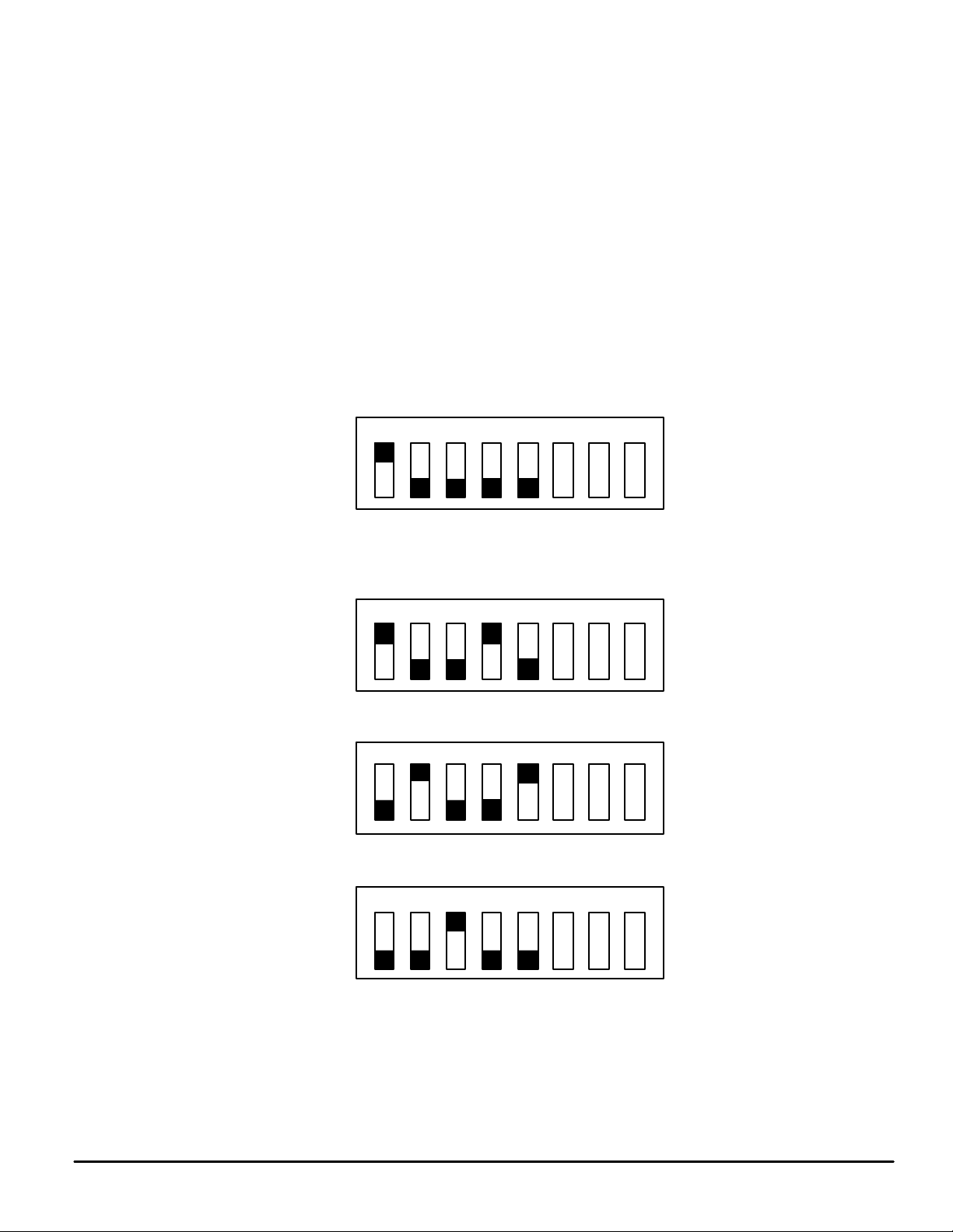
All boards have a DIP switch S1 which gives each a unique address. The configuration menu is used to
tell the program what type of board is connected at a board address. Switch positions for all possible
addresses are given in Figure 2.
Single Board Operation
Two– or Three–Board Cascade
1 2 3 4 5 6 7 8
Closed
Open
Board A
1 2 3 4 5 6 7 8
Closed
Open
Board B
1 2 3 4 5 6 7 8
Closed
Open
Board C
1 2 3 4 5 6 7 8
Closed
Open
Figure 2. Switch Positions

MC145192EVK • MC145202EVK
7
MOTOROLA
In Figure 2, DIP switch sections 6, 7, and 8 allow the computer to read Out A, Out B or Lock Detect from
the PLL device. Each of the inputs can only be read on one board at a time, but each item could be read
on a different board. In a three–board cascade, Out A could be read from the first board, Out B from the
second, and Lock Detect from the third. There is no way to determine in software the board address of a
particular input. The control program does not make use of these inputs. Pin assignment on the printer
port connector is:
Label
Pin Number
Out A 12
Out B 13
Lock Detect 15
PRINTER PORT CONFIGURATION
Printer port outputs on an IBM PC or clone use TTL–LS logic levels. Inputs are one TTL–LS load. Signal
lines can be used for any purpose. The standard names, direction of data flow, true and inverted data are
shown in Figure 3.
1
2
3
4
5
6
7
8
9
10
11
12
13
14
15
16
17
18 – 25
Printer
IBM Printer
Port
Pin Number
– Strobe
+ Data Bit 0
+ Data Bit 1
+ Data Bit 3
+ Data Bit 4
+ Data Bit 2
+ Data Bit 5
+ Data Bit 6
+ Data Bit 7
– Acknowledge
+ Busy
+ P. End (out of paper)
+ Select
– Auto Feed
– Error
– Initialize Printer
– Select Input
Ground
Signal Name
Figure 3. Printer Port Data Lines

MC145192EVK • MC145202EVK
MOTOROLA
8
Pin numbers for the port connector are shown in Figure 4.
1
13
14
25
(front view)
Figure 4. DB–25 Male Connector
MC145192EVK • MC145202EVK
9
MOTOROLA
SECTION 2 – SOFTWARE
INTRODUCTION
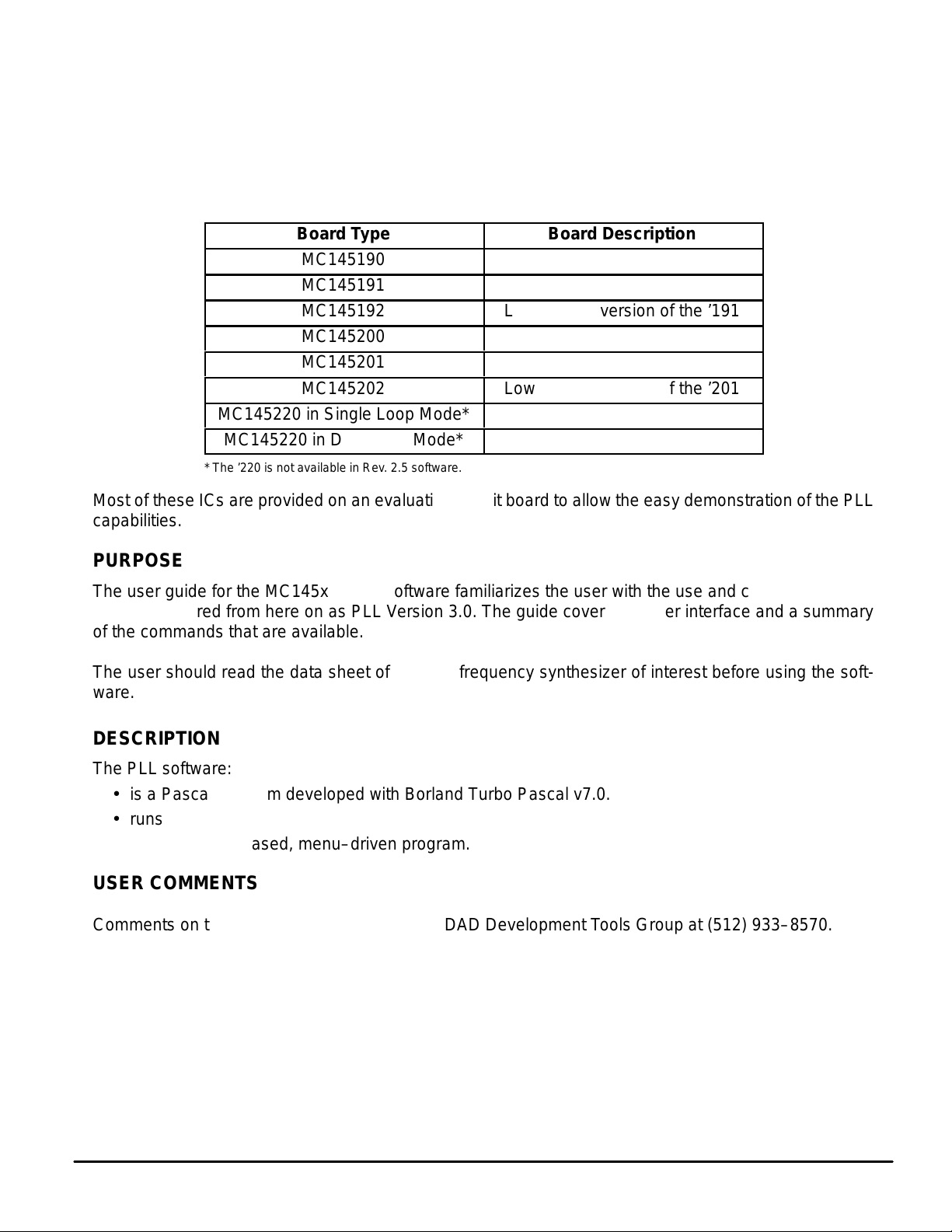
The MC145xxx PLL software is provided to demonstrate the capabilities of the MC145xxx family of PLLs.
The family includes the following devices:
Table 1.
Board Type
Board Description
MC145190
MC145191
MC145192
Low voltage version of the ’191
MC145200
MC145201
MC145202
Low voltage version of the ’201
MC145220 in Single Loop Mode*
MC145220 in Dual Loop Mode*
* The ’220 is not available in Rev. 2.5 software.
Most of these ICs are provided on an evaluation circuit board to allow the easy demonstration of the PLL
capabilities.
PURPOSE
The user guide for the MC145xxx PLL software familiarizes the user with the use and capabilities of the
program referred from here on as PLL Version 3.0. The guide covers the user interface and a summary
of the commands that are available.
The user should read the data sheet of the PLL frequency synthesizer of interest before using the software.
DESCRIPTION
The PLL software:
• is a Pascal program developed with Borland Turbo Pascal v7.0.
• runs under MS–DOS.
• is a character–based, menu–driven program.
USER COMMENTS
Comments on this program may be faxed to MDAD Development Tools Group at (512) 933–8570.

MC145192EVK • MC145202EVK
MOTOROLA
10
USER INTERFACE
The user interface consists of numerous character–based, menu–driven screens which are displayed
below. Each screen is shown, along with a description of its purpose.
CONVENTIONS
Some of the PLL screens are necessarily “busy”. Because of this, the program follows several conventions to help the user quickly absorb the screen information. These conventions are briefly described on
a help screen that is available throughout the program. Type the help command, [?], at any time to view
the help screen.
The conventions are as follows:
1. Command keys are surrounded by [ ]s. Type the letter between the [ ]s to execute the command.
[ ]s are followed by a description of the command.
2. [–] indicates a command not available to the user. Commands become available when they are
applicable to the currently targeted board.
3. [ ]s followed by an ! indicate the command will execute immediately. Otherwise a submenu is
displayed from which further choices may be made.
4. If no changes are desired to an input field, leave the field blank. The previous value will then be
used for that field. Type the TAB key to move to the next input field, or shift–TAB to move to the
prior input field. Type RETURN to store the new input values while remaining on the same screen.
Type Q to store the new values and return to the prior screen.
5. All numbers are entered as decimal values unless otherwise noted. A $ followed by a value indi–
cates the value is in hexadecimal format. The output port address is in hexadecimal format.
6. The second line from the top of screen (screen title) states the purpose of the screen.
7. Screen information that can be changed by the user is displayed in bold or reverse video.
8. Commands are case independent. X is the same as x.
9. Frequencies are entered as two numbers, and displayed as one. The two input numbers repre–
sent the desired frequency in MHz, and in kHz. These input values are added together to obtain
the final frequency. Leave either input field blank to retain the prior value for that portion of fre–
quency.

MC145192EVK • MC145202EVK
11
MOTOROLA
SCREENS
Screen #1 ‘Define boards to program’
The first screen the user sees when the program begins has a screen title of ‘Define boards to program’.
This screen is used to define which boards are connected to the LPT1 printer port of the computer. Refer
to the hardware setup section to determine how to cascade the evaluation boards.
This screen is also available from the main menu (screen #2). The user may return to this screen to
change the boards that are connected to the computer.
The screen is divided into two sections. The upper section shows the current board type settings while
the lower section allows the user to define a board’s type and position in the cascade connection.
Notice the section labeled ‘Available Boards:’ shows three labels, one for each board that may be cascaded. When the program first starts up it shows ‘N/A’ (not applicable) after each label. The user must
enter the boards contiguously. Initially the program requests for the user to enter board A’s type. This is
signified by
A
(in the screen below) being set to A. The user can the select the board type for board A by
typing the corresponding command.
Once board A’s type is selected,
A
automatically increments to B and the process may be repeated.
Once all boards have been correctly defined, the user may select [Q] which sends default data to the
boards and continues to the next screen. NOTE: Before selecting [Q], the user should insure that the
DIP switch settings shown in Figure 2 are correct.
If a board is incorrectly identified, select the board that is not correctly defined by typing the corresponding board letter ([A], [B], or [C]). The user may then reselect the board’s type. Once the board has been
identified, the user may select the letter ([A], [B], or [C]) of the board followed by [S] to change hardware–
dependent variables for that board. See screen #1b.
[X] can be selected to exit the program completely. [?] can be selected to view the help screen.
Welcome to MC145xxx EVK Demonstration Program, rev 2.5
Define boards to program
Available Boards:
Brd [A]!: N/A Brd [B]!: N/A Brd [C]!: N/A
––––––––––––––––––––––––––––––––––––––––––––––––––––––––––––––––––––––––––––––––
Board
A
is:
[–]! no board [4]! MC145200
[1]! MC145190 [5]! MC145201
[2]! MC145191 [6]! MC145202
[3]! MC145192
[–] Boards defined, Continue
[X]! Terminate demonstration program. [?]! View help screen.

MC145192EVK • MC145202EVK
MOTOROLA
12
Screen #1a Help Screen
Screen #1a is the help screen for the program. This screen is available from any point throughout the
program. A short list of the interface conventions are presented on this screen.
[X] can be selected to exit the program completely. [Q] can be selected to exit the help screen.
Welcome to MC145xxx EVK Demonstration Program, rev 2.5
1) Command keys are surrounded by []’s. Type the letter between the []’s to execute
the command. []’s are followed by a description of the command.
2) [–] indicates a command not available to the user.
3) []’s followed by an ! indicate the command will execute immediately. Otherwise a
sub menu will be displayed.
4) If no changes are desired to an input field, type the TAB key to move to the next
input field. The previous value will be used for that field.
5) All numbers are entered as decimal values unless otherwise noted. A $ followed by a
value indicates the value is in hexadecimal format.
6) The second line from the top of screen (screen title) states the purpose of the
screen.
7) Screen information that can be changed by the user is displayed in bold or reverse
video.
8) Commands are case independent. X is the same as x.
[X]! Terminate demonstration program. [Q]! Quit help screen.

MC145192EVK • MC145202EVK
13
MOTOROLA
Screen #2 ‘Select from the available options’
Screen #2 is the main screen of the program. This is where the user enters commands to demonstrate
the capabilities of the various boards connected to the computer. The title of the screen is ‘Select from
the available options’.
This screen is broken down into three sections:
Section #1, ‘Available Boards’
This section displays the board types that are connected to the computer. It also designates which
board is the currently selected ‘target’ board. This is the board that will receive the commands from
section #2. This section also provides the ability to change the targeted board. Type the target
board command ([A], [B], or [C]) to target that particular board.
Section #2, ‘MC145xxx Commands’
This section is further divided into three subsections. Each subsection contains commands that can
be sent to the ‘target’ board to demonstrate its capabilities. Each of these commands is described in
full in the Command Summary.
The first subsection, ‘MC145xxx Frequency Commands’, contains commands that are
used to modify the PLL frequency in some way . These commands are available for all possible target board types.
In the top line of this section, ‘Current Output Frequency is
746 MHz’
designates what the
frequency is for the currently targeted board. This value is dynamic.
On the lines below this,
741 MHz
is the current setting for the default low frequency.
746 MHz
is the current setting for the default medium frequency.
751 MHz is
the current
setting for the default high frequency.
The second subsection, ‘MC145xxx Additional Commands’, contains commands that
are used to further modify the currently targeted board. These commands also work with all
of the MC145xxx board types.
The third subsection, ‘MC145220 EVK – Single Specific Commands’, are only displayed when the MC145220EVK in single loop mode is the currently targeted board. This
section shows commands that are specific to this board. This is required since this board
contains the equivalent of two PLLs.
The command letter for ‘Set target PLL on board’ is [T]!. In single loop mode, the user may
toggle between PLL and PLL’ on the MC145220EVK by using this command. Feedback is
given to the user as to whether PLL or PLL’ will be accessed. See near the top of the screen
on the line titled “Available Boards - Current target board is: ...”
Section #3, ‘Initialization/System Setup Commands’
This section contains commands that are used to initialize all boards connected to the computer or
to set up the computer.

MC145192EVK • MC145202EVK
MOTOROLA
14
Screen #2 ‘Select from the available options’ (continued)
Welcome to MC145xxx EVK Demonstration Program, rev 2.5
Select from the available options
Available Boards – Current target board is: A, MC145190
Brd [A]!: MC145190 Brd [–]!: N/A Brd [–]!: N/A
––––––––––––––––––––––––––––––––––––––––––––––––––––––––––––––––––––––––––––––––
MC145xxx Frequency Commands – Current Output Frequency is
746 MHz
[L]! Set to low freq
741 MHz
[W] Change default low freq.
[M]! Set to med. freq
746 MHz
[Y] Change default med. freq.
[H]! Set to high freq.
751 MHz
[Z] Change default high freq.
[U]! Step frequency up by step size [O] Set PLL output frequency
[D]! Step frequency down by step size [F] Set REFin freq. & channel spacing
MC145xxx Additional Commands
[E] Set function of output A [N] Change C Register
[R] Set crystal/reference mode – Current mode is Ref. mode, REFout low
––––––––––––––––––––––––––––––––––––––––––––––––––––––––––––––––––––––––––––––––
Initialization/System Setup Commands:
[P] Set output port address – Current address is $278
[G] Change board definitions
[I] Initialize board(s), Write all registers
[X]! Terminate demonstration program. [?]! View help screen.

MC145192EVK • MC145202EVK
15
MOTOROLA
Screen #3 After [O] Command Selected
This is the resulting screen that is displayed after the user selects the ‘[O] Set PLL output frequency’
command. The user is prompted to enter the new frequency.
The current output frequency is automatically retained if the user hits return or [Q] without entering a
value.
Welcome to MC145xxx EVK Demonstration Program, rev 2.5
Set PLL output frequency
Available Boards – Current target board is: A, MC145190
Brd [A]!: MC145190 Brd [–]!: N/A Brd [–]!: N/A
––––––––––––––––––––––––––––––––––––––––––––––––––––––––––––––––––––––––––––––––
Input new frequency in integer values of MHz and kHz.
Original program default PLL output frequency is 746 MHz
Current PLL output frequency is 746 MHz
Current frequency range is 741 MHz to 751 MHz
Frequencies outside this range will be accepted.
New PLL frequency: 746 MHz + 000 kHz
[TAB] to move to next field
[Q] to return to main menu
[X]! Terminate demonstration program. [?]! View help screen.
 Loading...