

Motorola MC14500BCL, MC14500BCP, MC14500BDW Datasheet
MOTOROLA CMOS LOGIC DATAMC14500B
306
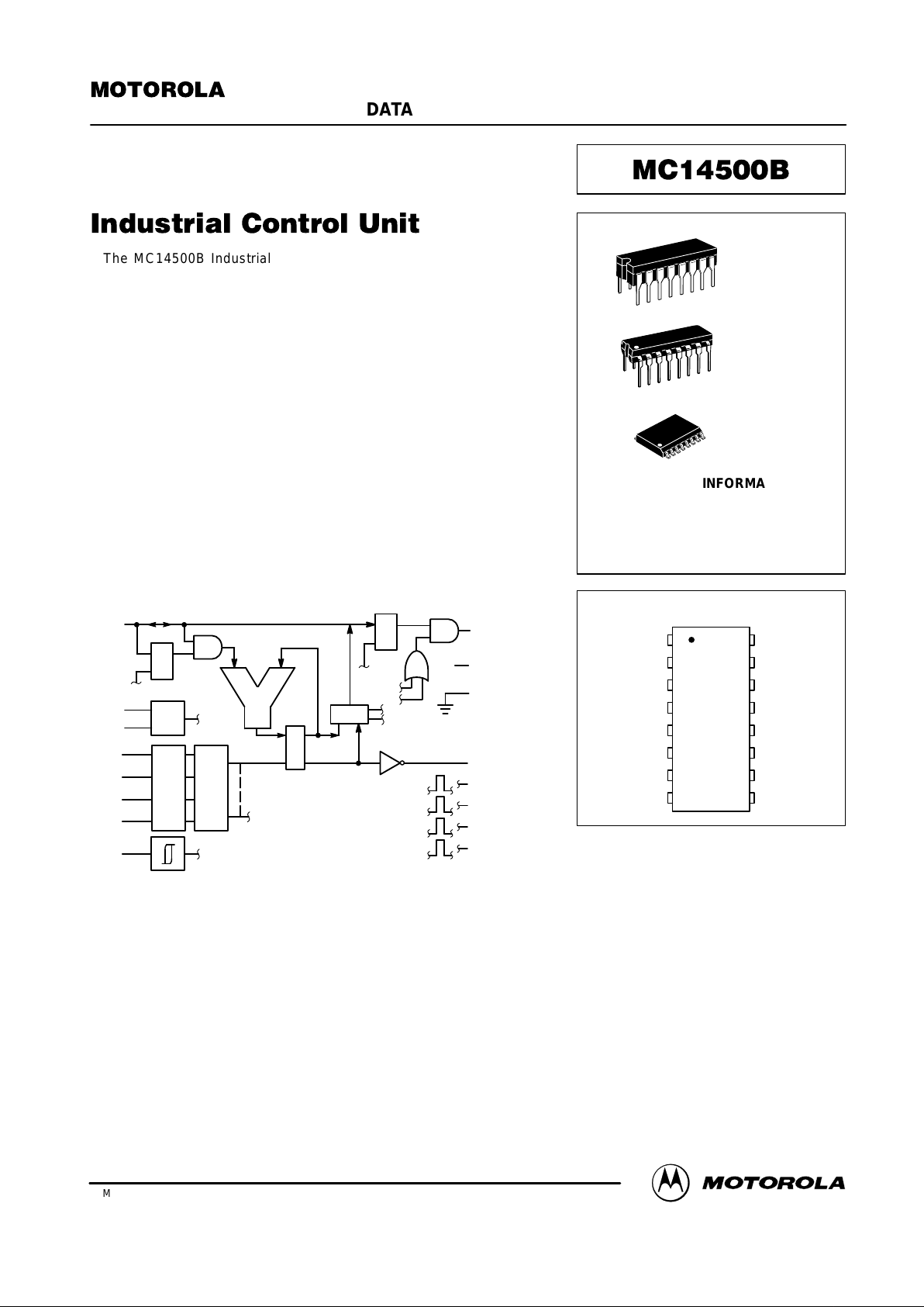
The M C14500B I ndustrial C ontrol Unit (ICU) i s a single–bit C MOS
processor. The ICU is designed for use in systems requiring decisions based
on successive single–bit information. An external ROM stores the control
program. With a program counter (and output latches and input multiplexers,
if required) the ICU in a system forms a stored–program controller that
replaces combinatorial logic. Applications include relay logic processing,
serial data manipulation and control. The ICU also may control an MPU or be
controlled by an MPU.
• 16 Instructions
• DC to 1.0 MHz Operation at VDD = 5 V
• On–Chip Clock (Oscillator)
• Executes One Instruction per Clock Cycle
• 3 to 18 V Operation
• Low Quiescent Current Characteristic of CMOS Devices
• Capable of Driving One Low–Power Schottky Load or Two Low–Power
TTL Loads over Full Temperature Range
BLOCK DIAGRAM
DATA
X1
X2
I0
I1
I2
I3
RST
3
14
13
7
6
5
4
1
INST
REG
OSC
D
C
IEN
LU
D
C
RESULT
REG. (RR)
MUX
D
C
16
2
8
WRITE
V
DD
V
SS
15
12
11
10
9
RR
JMP
RTN
FLAG O
FLAG F
+V
OEN
STOC
STO
X1 — OSCILLATOR OUTPUT
X2 — OSCILLATOR INPUT
SEMICONDUCTOR TECHNICAL DATA
Motorola, Inc. 1995
REV 3
1/94
L SUFFIX
CERAMIC
CASE 620
ORDERING INFORMATION
TA = – 55° to 125°C for all packages.
P SUFFIX
PLASTIC
CASE 648
DW SUFFIX
SOIC
CASE 751G
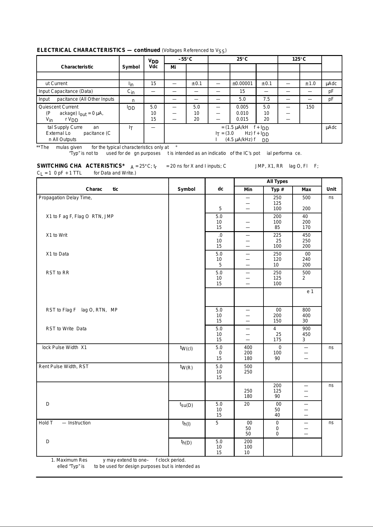
PIN ASSIGNMENT
MC14XXXBCP Plastic
MC14XXXBCL Ceramic
MC14XXXBDW SOIC
13
14
15
16
9
10
11
125
4
3
2
1
8
7
6
JMP
X2
X1
V
DD
FLAG F
FLAG O
RTN
I3
DATA
WRITE
RST
V
SS
I0
I1
I2
RR
MOTOROLA CMOS LOGIC DATA
307
MC14500B
MAXIMUM RATINGS* (Voltages Referenced to V
SS
)
Symbol
Parameter
Value
Unit
V
DD
DC Supply Voltage
– 0.5 to + 18.0
V
Vin, V
out
Input or Output Voltage (DC or Transient)
– 0.5 to VDD + 0.5
V
Iin,
Iout
Input or Output Current (DC or Transient),
per Pin
± 10
mA
P
D
Power Dissipation, per Package†
500
mW
T
stg
Storage Temperature
– 65 to + 150
_
C
T
L
Lead Temperature (8–Second Soldering)
260
_
C
*Maximum Ratings are those values beyond which damage to the device may occur.
†Temperature Derating:
Plastic “P and D/DW” Packages: – 7.0 mW/_C From 65_C To 125_C
Ceramic “L” Packages: – 12 mW/_C From 100_C To 125_C
ELECTRICAL CHARACTERISTICS (Voltages Referenced to V
SS
)
V
– 55_C
25_C
125_C
Characteristic
Symbol
V
DD
Vdc
Min
Max
Min
Typ #
Max
Min
ÎÎÎ
ÎÎÎ
ÎÎÎ
Max
Unit
Output Voltage
“0” Level
Vin = VDD or 0
V
OL
5.0
10
15
—
—
—
0.05
0.05
0.05
—
—
—
0
0
0
0.05
0.05
0.05
—
—
—
ÎÎÎ
ÎÎÎ
ÎÎÎ
ÎÎÎ
0.05
0.05
0.05
Vdc
“1” Level
Vin = 0 or V
DD
V
OH
5.0
10
15
4.95
9.95
14.95
—
—
—
4.95
9.95
14.95
5.0
10
15
—
—
—
4.95
9.95
14.95
ÎÎÎ
ÎÎÎ
ÎÎÎ
ÎÎÎ
—
—
—
Vdc
Input Voltage
“0” Level
RST, D, X2
(VO = 4.5 or 0.5 Vdc)
(VO = 9.0 or 1.0 Vdc)
(VO = 13.5 or 1.5 Vdc)
V
IL
5.0
10
15
—
—
—
1.5
3.0
4.0
—
—
—
2.25
4.50
6.75
1.5
3.0
4.0
—
—
—
ÎÎÎ
ÎÎÎ
ÎÎÎ
ÎÎÎ
ÎÎÎ
ÎÎÎ
1.5
3.0
4.0
Vdc
“1” Level
(VO = 0.5 or 4.5 Vdc)
(VO = 1.0 or 9.0 Vdc)
(VO = 1.5 or 13.5 Vdc)
V
IH
5.0
10
15
3.5
7.0
11
—
—
—
3.5
7.0
11
2.75
5.50
8.25
—
—
—
3.5
7.0
11
ÎÎÎ
ÎÎÎ
ÎÎÎ
ÎÎÎ
—
—
—
Vdc
Input Voltage #
“0” Level
I0, I1, I2, I3
(VO = 4.5 or 0.5 Vdc)
(VO = 9.0 or 1.0 Vdc)
(VO = 13.5 or 1.5 Vdc)
V
IL
5.0
10
15
—
—
—
0.8
1.6
2.4
—
—
—
1.1
2.2
3.4
0.8
1.6
2.4
—
—
—
ÎÎÎ
ÎÎÎ
ÎÎÎ
ÎÎÎ
ÎÎÎ
ÎÎÎ
0.8
1.6
2.4
Vdc
“1” Level
(VO = 0.5 or 4.5 Vdc)
(VO = 1.0 or 9.0 Vdc)
(VO = 1.5 or 13.5 Vdc)
V
IH
5.0
10
15
2.0
6.0
10
—
—
—
2.0
6.0
10
1.9
3.1
4.3
—
—
—
2.0
6.0
10
ÎÎÎ
ÎÎÎ
ÎÎÎ
ÎÎÎ
ÎÎÎ
—
—
—
Vdc
Output Drive Current Source
Data, Write
(VOH = 4.6 Vdc)
(VOH = 9.5 Vdc)
(VOH = 13.5 Vdc)
I
OH
5.0
10
15
– 1.2
– 3.6
– 7.2
—
—
—
– 1.0
– 3.0
– 6.0
– 2.0
– 6.0
– 12
—
—
—
– 0.7
– 2.1
– 4.2
ÎÎÎ
ÎÎÎ
ÎÎÎ
ÎÎÎ
ÎÎÎ
—
—
—
mAdc
(VOL = 0.4 Vdc) Sink
(VOL = 0.5 Vdc)
(VOL = 1.5 Vdc)
I
OL
5.0
10
15
1.9
3.6
7.2
—
—
—
1.6
3.0
6.0
3.2
6.0
12
—
—
—
1.1
2.1
4.2
ÎÎÎ
ÎÎÎ
ÎÎÎ
ÎÎÎ
ÎÎÎ
—
—
—
mAdc
Output Drive Current Source
Other Outputs
(VOH = 2.5 Vdc)
(VOH = 4.6 Vdc)
(VOH = 9.5 Vdc)
(VOH = 13.5 Vdc)
I
OH
5.0
5.0
10
15
– 3.0
– 0.64
– 1.6
– 4.2
—
—
—
—
– 2.4
– 0.51
– 1.3
– 3.4
– 4.2
– 0.88
– 2.25
– 8.8
—
—
—
—
– 1.7
– 0.36
– 0.9
– 2.4
ÎÎÎ
ÎÎÎ
ÎÎÎ
ÎÎÎ
ÎÎÎ
ÎÎÎ
—
—
—
—
mAdc
(VOL = 0.4 Vdc) Sink
(VOL = 0.5 Vdc)
(VOL = 1.5 Vdc)
I
OL
5.0
10
15
0.64
1.6
4.2
—
—
—
0.51
1.3
3.4
0.88
2.25
8.8
—
—
—
0.36
0.9
2.4
ÎÎÎ
ÎÎÎ
ÎÎÎ
ÎÎÎ
—
—
—
mAdc
#Data labelled “Typ” is not to be used for design purposes but is intended as an indication of the IC’s potential performance.
This device contains protection circuitry to
guard against damage due to high static
voltages or electric fields. However, precautions must be taken to avoid applications of
any voltage higher than maximum rated voltages to this high–impedance circuit. For proper
operation, Vin and V
out
should be constrained
to the range VSS v (Vin or V
out
) v VDD.
Unused inputs must always be tied to an
appropriate logic voltage level (e.g., either V
SS
or VDD). Unused outputs must be left open.
MOTOROLA CMOS LOGIC DATAMC14500B
308
ELECTRICAL CHARACTERISTICS — continued (Voltages Referenced to V
SS
)
V
–55_C
25_C
125_C
Characteristic
Symbol
V
DD
Vdc
Min
Max
Min
Typ #
Max
Min
ÎÎÎ
ÎÎÎ
ÎÎÎ
Max
Unit
Input Current, RST
I
in
15
25
—
—
150
—
—
ÎÎÎ
ÎÎÎ
ÎÎÎ
250
µAdc
Input Current
I
in
15
—
± 0.1
—
±0.00001
± 0.1
—
ÎÎÎ
ÎÎÎ
± 1.0
µAdc
Input Capacitance (Data)
C
in
—
—
—
—
15
—
—
ÎÎÎ
ÎÎÎ
ÎÎÎ
—
pF
Input Capacitance (All Other Inputs)
C
in
—
—
—
—
5.0
7.5
—
ÎÎÎ
ÎÎÎ
ÎÎÎ
—
pF
Quiescent Current
(Per Package) I
out
= 0 µA,
Vin = 0 or V
DD
I
DD
5.0
10
15
—
—
—
5.0
10
20
—
—
—
0.005
0.010
0.015
5.0
10
20
—
—
—
ÎÎÎ
ÎÎÎ
ÎÎÎ
ÎÎÎ
150
300
600
µAdc
**Total Supply Current at an
External Load Capacitance (CL)
on All Outputs
I
T
—
IT = (1.5 µA/kHz) f + I
DD
IT = (3.0 µA/kHz) f + I
DD
IT = (4.5 µA/kHz) f + I
DD
µAdc
**The formulas given are for the typical characteristics only at 25_C.
#Data labelled “Typ” is not to be used for design purposes but is intended as an indication of the IC’s potential performance.
SWITCHING CHARACTERISTICS* (T
A
= 25_C; tr = tf = 20 ns for X and I inputs; CL = 50 pF for JMP, X1, RR, Flag O, Flag F;
CL = 130 pF + 1 TTL load for Data and Write.)
ÎÎÎÎ
ÎÎÎÎ
ÎÎÎÎ
V
ОООООООООО
ОООООООООО
ОООООООООО
All Types
Characteristic
ÎÎÎÎ
ÎÎÎÎ
ÎÎÎÎ
Symbol
V
DD
Vdc
ÎÎÎÎ
ÎÎÎÎ
ÎÎÎÎ
Min
Typ #
Max
Unit
Propagation Delay Time, X1 to RR
ÎÎÎÎ
ÎÎÎÎ
ÎÎÎÎ
ÎÎÎÎ
t
PLH
,
t
PHL
5.0
10
15
ÎÎÎÎ
ÎÎÎÎ
ÎÎÎÎ
ÎÎÎÎ
—
—
—
250
125
100
500
250
200
ns
X1 to Flag F, Flag O, RTN, JMP
ÎÎÎÎ
ÎÎÎÎ
ÎÎÎÎ
ÎÎÎÎ
5.0
10
15
ÎÎÎÎ
ÎÎÎÎ
ÎÎÎÎ
ÎÎÎÎ
—
—
—
200
100
85
400
200
170
X1 to Write
ÎÎÎÎ
ÎÎÎÎ
ÎÎÎÎ
ÎÎÎÎ
5.0
10
15
ÎÎÎÎ
ÎÎÎÎ
ÎÎÎÎ
ÎÎÎÎ
—
—
—
225
125
100
450
250
200
X1 to Data
ÎÎÎÎ
ÎÎÎÎ
ÎÎÎÎ
ÎÎÎÎ
5.0
10
15
ÎÎÎÎ
ÎÎÎÎ
ÎÎÎÎ
ÎÎÎÎ
—
—
—
250
120
100
500
240
200
RST to RR
ÎÎÎÎ
ÎÎÎÎ
ÎÎÎÎ
ÎÎÎÎ
5.0
10
15
ÎÎÎÎ
ÎÎÎÎ
ÎÎÎÎ
ÎÎÎÎ
—
—
—
250
125
100
500
250
200
RST to X1
ÎÎÎÎ
ÎÎÎÎ
ÎÎÎÎ
ÎÎÎÎ
5.0
10
15
ÎÎÎÎ
ÎÎÎÎ
ÎÎÎÎ
ÎÎÎÎ
—
—
—
450
200
150
Note 1
RST to Flag F, Flag O, RTN, JMP
ÎÎÎÎ
ÎÎÎÎ
ÎÎÎÎ
ÎÎÎÎ
5.0
10
15
ÎÎÎÎ
ÎÎÎÎ
ÎÎÎÎ
ÎÎÎÎ
—
—
—
400
200
150
800
400
300
RST to Write, Data
ÎÎÎÎ
ÎÎÎÎ
ÎÎÎÎ
ÎÎÎÎ
5.0
10
15
ÎÎÎÎ
ÎÎÎÎ
ÎÎÎÎ
ÎÎÎÎ
—
—
—
450
225
175
900
450
350
Clock Pulse Width, X1
ÎÎÎÎ
ÎÎÎÎ
ÎÎÎÎ
ÎÎÎÎ
t
W(cl)
5.0
10
15
ÎÎÎÎ
ÎÎÎÎ
ÎÎÎÎ
ÎÎÎÎ
400
200
180
200
100
90
—
—
—
ns
Rent Pulse Width, RST
ÎÎÎÎ
ÎÎÎÎ
ÎÎÎÎ
ÎÎÎÎ
t
W(R)
5.0
10
15
ÎÎÎÎ
ÎÎÎÎ
ÎÎÎÎ
ÎÎÎÎ
500
250
200
250
125
100
—
—
—
ns
Setup Time — Instruction
ÎÎÎÎ
ÎÎÎÎ
ÎÎÎÎ
ÎÎÎÎ
t
su(l)
5.0
10
15
ÎÎÎÎ
ÎÎÎÎ
ÎÎÎÎ
ÎÎÎÎ
400
250
180
200
125
90
—
—
—
ns
Data
ÎÎÎÎ
ÎÎÎÎ
ÎÎÎÎ
ÎÎÎÎ
t
su(D)
5.0
10
15
ÎÎÎÎ
ÎÎÎÎ
ÎÎÎÎ
ÎÎÎÎ
200
100
80
100
50
40
—
—
—
Hold Time — Instruction
ÎÎÎÎ
ÎÎÎÎ
ÎÎÎÎ
ÎÎÎÎ
t
h(l)
5.0
10
15
ÎÎÎÎ
ÎÎÎÎ
ÎÎÎÎ
ÎÎÎÎ
100
50
50
0
0
0
—
—
—
ns
Data
ÎÎÎÎ
ÎÎÎÎ
ÎÎÎÎ
ÎÎÎÎ
t
h(D)
5.0
10
15
ÎÎÎÎ
ÎÎÎÎ
ÎÎÎÎ
ÎÎÎÎ
200
100
100
100
50
50
—
—
—
NOTE 1. Maximum Reset Delay may extend to one–half clock period.
#Data labelled “Typ” is not to be used for design purposes but is intended as an indication of the IC’s potential performance.
 Loading...