

Motorola MC145003FU, MC145004FU Datasheet
SEMICONDUCTOR TECHNICAL DATA
Order this document
by MC145003/D
Product Preview
CMOS
The MC145003/5004 are 128–segment, multiplexed–by–four LCD Drivers.
The two devices are functionally the same except for their data input protocols. The MC145003 uses an SPI data input protocol which is directly compatible with that of the MC6805 family of microcomputers. Using a minimal
amount of software (see example), the device may be interfaced to the
MC68HCXX product families. The MC145004 has a IIC interface and has essentially the same protocol, except that the device sends an acknowledge bit
back to the transmitter after each eight–bit byte is received. MC145004 also
has a “read mode”, whereby data sent to the device may be retrieved via the
IIC bus.
The MC145003/MC145004 drives the liquid–crystal displays in a multiplexed–by–four configuration. The device accepts data from a microprocessor or other serial data source to drive one segment per bit. The chip does not
have a decoder, allowing for the flexibility of formatting the segment data
externally.
Devices are independently addressable via a two–wire (or three–wire)
communication link which can be common with other MC145003/MC145004
and/or other peripheral devices.
• Drives 128 Segments Per Package
• Devices May Be Cascaded for Larger LCD Applications
• May Be Used with the Following LCDs: Segmented Alphanumeric,
Bar Graph, Dot Matrix, Custom
• Quiscent Supply Current: 85 µA @ 2.8 V V
• Operating Voltage Range: 2.8 to 5.5 V
• Operating Temperature Range: –40 to 85°C
• Separate Access to LCD Drive Section’s Supply Voltage to Allow for
Temperature Compensation
• See Application Notes AN1066 and AN442
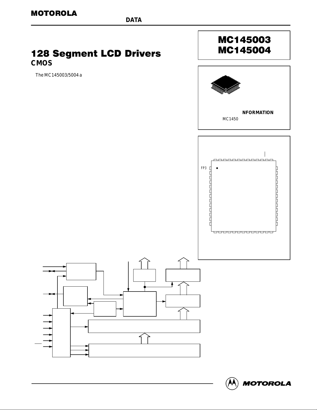
BLOCK DIAGRAM
DD
1
52
ORDERING INFORMATION
MC145003FU QFP
MC145004FU QFP
PIN ASSIGNMENT
DD
V
NC
OSC1
OSC2
BP1
BP2
52 51 50 49 48 47 46 45 44 43 42 41 40
FP32
1
FP31
2
FP30
3
FP29
4
FP28
5
FP27
6
FP26
7
FP25
8
FP24
9
FP23
10
FP22
11
FP21
12
FP20
13
14 15 16 17 18 19 20 21 22 23 24 25 26
NC
FP19
FP18
FP17
FP16
FP15
V
FU SUFFIX
CASE 848B
BP4A0A1A2ENB
BP3
SS
V
LCD
FP14
FP13
QFP
FP12
NC
39
D
in
38
DCLK
37
FS
36
FP1
35
FP2
34
FP3
33
FP4
32
FP5
31
FP6
30
FP7
29
FP8
28
FP9
27
FP10
NC
FP11
BP1–BP4 FP1–FP32
V
LCD
OSC1
OSC2
FS
DCLK
D
in
A0
A1
A2
ENB
This document contains information on a new product under development. Motorola reserves the right to change or discontinue this product without notice.
Motorola, Inc. 1994
OSCILLA TOR
FRAME
SYNC
GENERAT OR
DATA AND ADDRESS
CONTROL AND TIMING
POR
DRIVERS DRIVERS
LCD VOLTAGE
WAVEFORM
AND TIMING
GENERAT OR
128–BIT LATCH
128–BIT SHIFT REGISTER
128 – 32
MULTIPLEX
REV 1
12/94
NC = NO CONNECTION
ABSOLUTE MAXIMUM RATINGS (Voltages Referenced to V
V
DD
V
LCD
Symbol
V
DD
V
in
Vin
osc
I
in
T
stg
DC Supply Voltage – 0.5 to + 6.5 V
Input Voltage, Din, and Data Clock – 0.5 to 15 V
Input Voltage, OSCin of Master – 0.5 to VDD + 0.5 V
DC Input Current, per Pin ± 10 mA
Storage Temperature Range – 65 to + 150 °C
Parameter Value Unit
SS
)
*Maximum Ratings are those values beyond which damage to the device may occur . Func-
tional operation should be restricted to the limits in the Electrical Characteristics tables or
Pin Descriptions section.
This device contains protection circuitry
to guard against damage due to high static
voltages or electric fields. However, precautions must be taken to avoid applications of
any voltage higher than maximum rated
voltages to this high–impedance circuit.
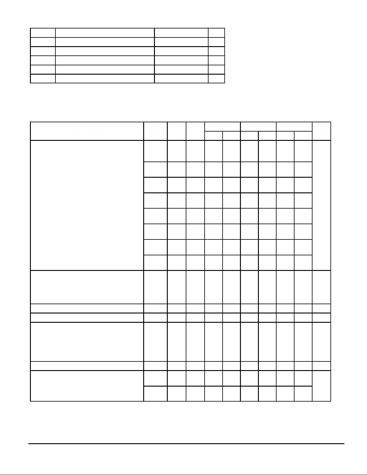
ELECTRICAL CHARACTERISTICS (Voltages Referenced to V
Characteristic Symbol
Output Drive Current — Frontplanes
Supply Currents (f
Input Current I
Input Capacitance C
Frequencies
OSC2 Frequency @ R1; R1 = 200 kΩ
OSC2 Frequency @ R2; R2 = 996 kΩ
Average DC Offset Voltage (BP Relative to FP) V
Input Voltage “0” Level V
) = 110 kHz
OSC
IDD = Quiescent @ I
I
= Quiescent @ I
LCD
IDD = Quiescent @ I
I
= Quiescent @ I
LCD
VO = 0.15 V
VO = 2.65 V I
VO = 1.72 V I
VO = 1.08 V I
VO = 0.15 V I
VO = 5.35 V I
VO = 3.52 V I
VO = 1.98 V I
= 0 µA
out
= 0 µA
out
= 0 µA
out
= 0 µA
out
FS Frequency @ R1
FS Pulse @ R1
BP Frequency @ R1
“1” Level V
I
FH
I
FL
FH
I
FL
FH
I
FL
FH
I
FL
FH
I
FL
FH
I
FL
FH
I
FL
FH
I
FL
I
DDQ
I
LCDQ
I
DDQ
I
LCDQ
in
f
OSC2
f
FS
f
FS
f
BP
f
OSC2
OO
V
IH
V
IH
in
IL
IL
)
SS
V
V
V
5
5
5
5
5
5
5
5
5
5
5
5
5
5
5
5
2.8
—
5.5
—
— — — — –0.1 0.1 — — µA
— — — — — 7.5 — — pF
5
5
5
5
5
5 2.8 –50 +50 –50 +50 –50 +50 mV
2.8
5.5
2.8
5.5
V
2.8
2.8
2.8
2.8
2.8
2.8
2.8
2.8
5.5
5.5
5.5
5.5
5.5
5.5
5.5
5.5
—
2.8
—
5.5
5
5
5
5
5
5
5
5
5
–40°C 25°C 85°C
Min Max Min Max Min Max
360
360——
–320
–320——
–95——
–1.5
90
—
600
600——
–490
–490——
–100——
–1.5
100——
—
—
—
—
103
100
4.7
100
22.5
24.5
—
—
—
—
260
260——
–240
–240——
–40——
—
40
2
—
600
600——
–520
–520——
–35——
1.555—
65
30
350
60
111
110
110
—
—
—
—
100
100
5
3.6
100
23
—
——0.85
—
—
—23.85——
240
240——
–240
–240——
—
2
—
1
140
45
90
150
140
5.6
140
33
–60——
580
580——
–520
–520——
–50——
123
120
120
–1.5
–1.5
1050
1.65——
55
—
70
—
—
—
—
—
3.5
28
—
—
350
136
133
133
–1
—
1
–1
—
1
85
20
35
3.9
31
—
—
—
—
(continued)
Unit
µA
µA
kHz
Hz
µs
Hz
kHz
V
MC145003 • MC145004 MOTOROLA
2
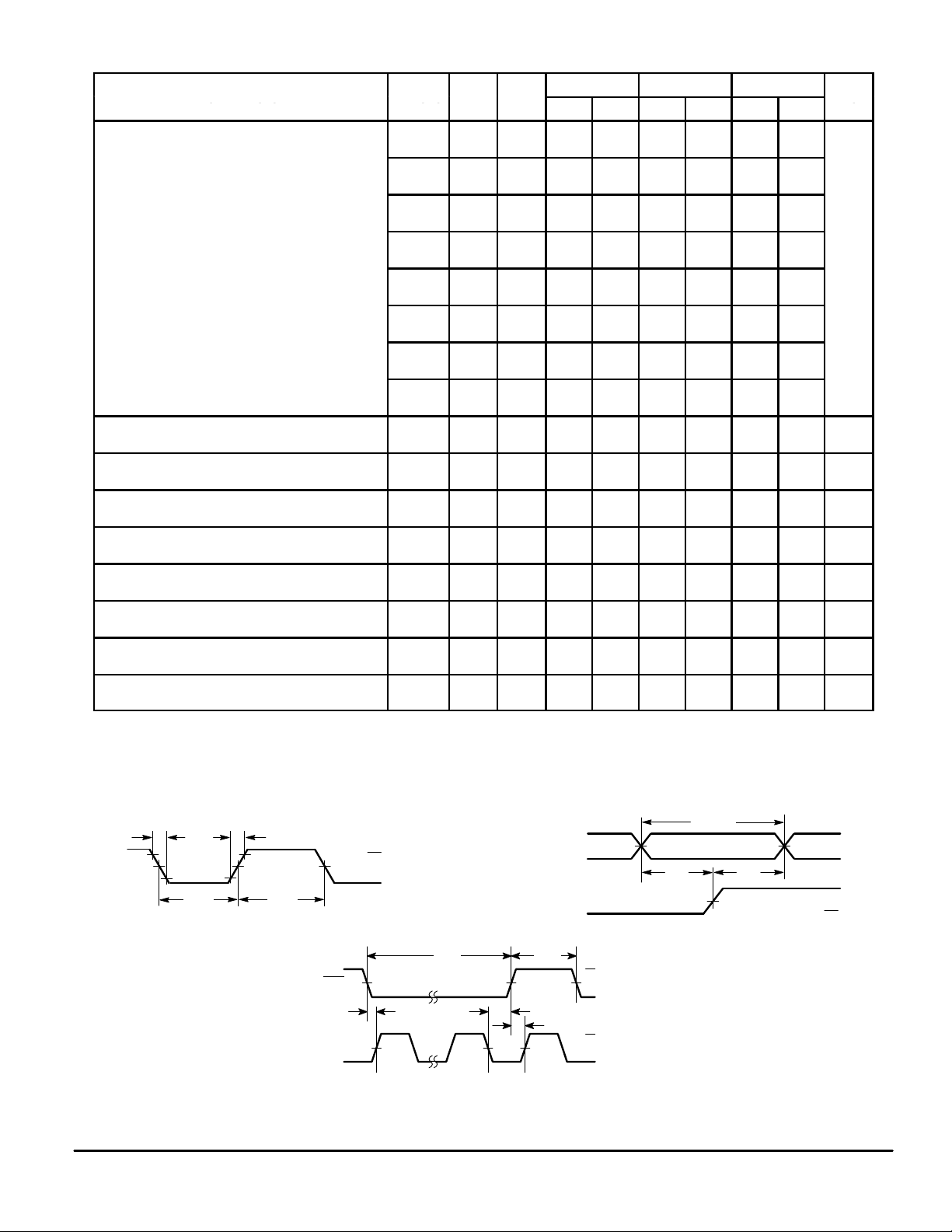
ELECTRICAL CHARACTERISTICS (Continued)
V
DD
V
LCD
40°C 25°C 85°C
Characteristic Symbol
Output Drive Current — Backplanes VO = 2.65 V IBH*
VO = 0.15 V I
VO = 1.08V I
VO = 1.72 V I
VO = 5.35 V I
VO = 0.15 V I
VO = 1.98 V I
VO = 3.52 V I
Pulse Width, Data Clock (Figure 1) t
DCLK Rise/Fall Time (Figure 1) tr, t
Setup Time, Din to DCLK (Figure 2) t
Hold Time, Din to DCLK (Figure 2) t
DCLK Low to ENB High (Figure 3) t
ENB High to DCLK High (Figure 3) t
ENB High Pulse Width (Figure 3) t
ENB Low to DCLK High (Figure 3) t
NOTE: Timing for Figures 1, 2, and 3 are design estimates only.
* For a time (t = 4/OSC FREQ.) after the backplane waveform changes to a new voltage level, the circuit is maintained in the high–current state
to allow the load capacitances to charge quickly. The circuit is then returned to the low–current state until the next voltage change.
I
I
I
I
I
I
I
I
BL
BH
BL
BH
BL
BH
BL
BH
BL
BH
BL
BH
BL
BH
BL
w
su
h
h
rec
w
su
V
5
5
5
5
5
5
5
5
5
5
5
5
5
5
5
5
5
3
5
f
3
5
3
5
3
5
3
5
3
5
3
5
3
V
Min Max Min Max Min Max
2.8
–290
2.8
–290——
2.8
310
2.8
310——
2.8
2.8
2.8
2.8
5.5
5.5
5.5
5.5
5.5
5.5
5.5
5.5
90
—
–90——
–490
–490——
600
600——
100——
–100——–1–35——–1–50——
—
1
–1.5
1.555—
–240
–240——
260
260——
40
—
–40——–1–60——
–520
–520——
600
600——
50
100——
—
—20120
30
60
10
20
10
20
50
100——
10
20
—
2
—
1
0
—
0
—
—
—
—
—
—
—
—
—
–240
–240——
230
230——
55
—
–1
–520
–520——
580
580——
70
—
–1
Unit
µA
—
1
—
1
ns
µs
ns
ns
ns
ns
ns
ns
90%
CLK
50%
10%
MOTOROLA
t
f
t
w
t
r
t
w
Figure 1.
ENB
CLK
SWITCHING WAVEFORMS
V
DD
GND
50%
50%
FIRST
CLK
t
su
t
w
LAST
CLK
Figure 3.
t
w
t
h
t
D
CLK
rec
VALID
in
50%
t
su
50%
t
h
V
DD
GND
V
DD
GND
Figure 2.
V
DD
GND
V
DD
GND
MC145003 • MC145004
3
FUNCTIONAL DESCRIPTION
The MC145003/MC145004 has essentially two sections
which operate asynchronously from each other; the data input
and storage section and the LCD drive section. The LCD drive
and timing is derived from the oscillator, while the data input
and storage is controlled by the Data In (Din), Data Clock
(DCLK), Address (A0, A1, A2), and Enable (ENB
) pins.
Data is shifted serially into the 128–bit shift register and
arranged into four consecutive blocks of 32 parallel data bits.
A time–multiplex of the four backplane drivers is made (each
backplane driver becoming active then inactive one after
another) and, at the start of each backplane active period, the
corresponding block of 32 bits is made available at the frontplane drivers. A high input to a plane driver turns the driver on,
and a low input turns the driver off.
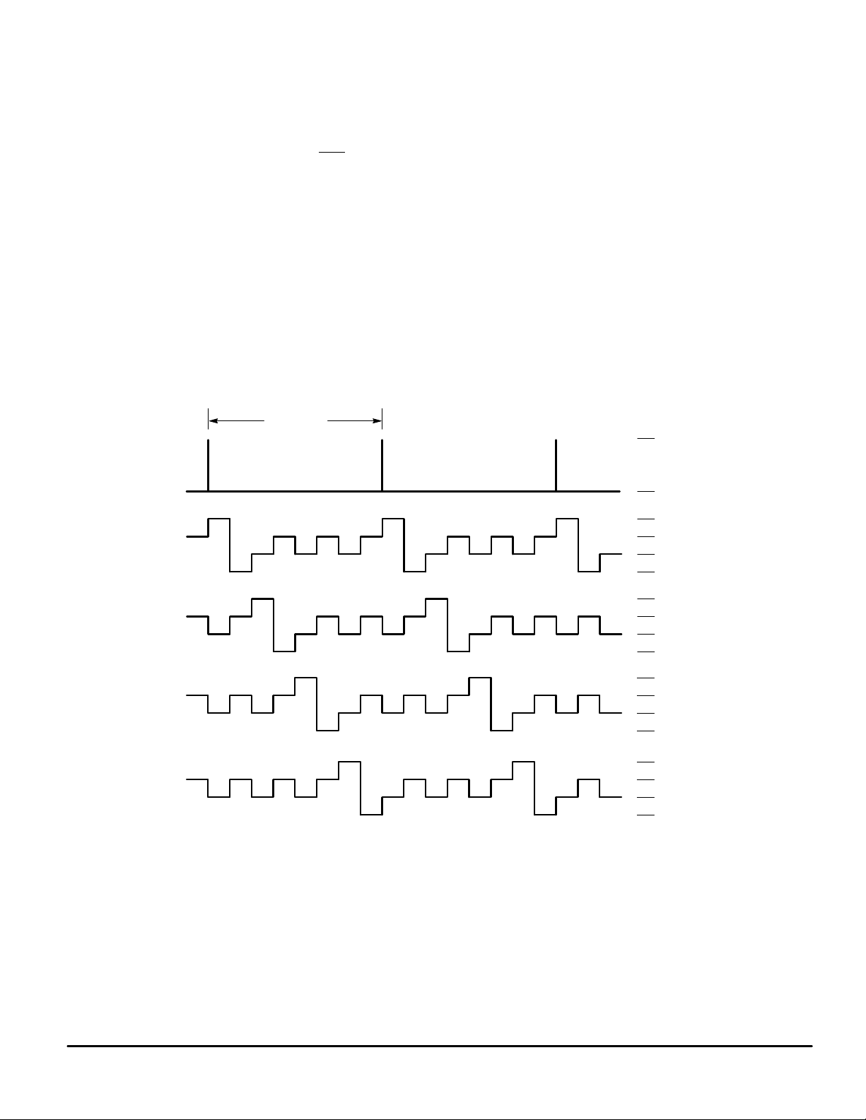
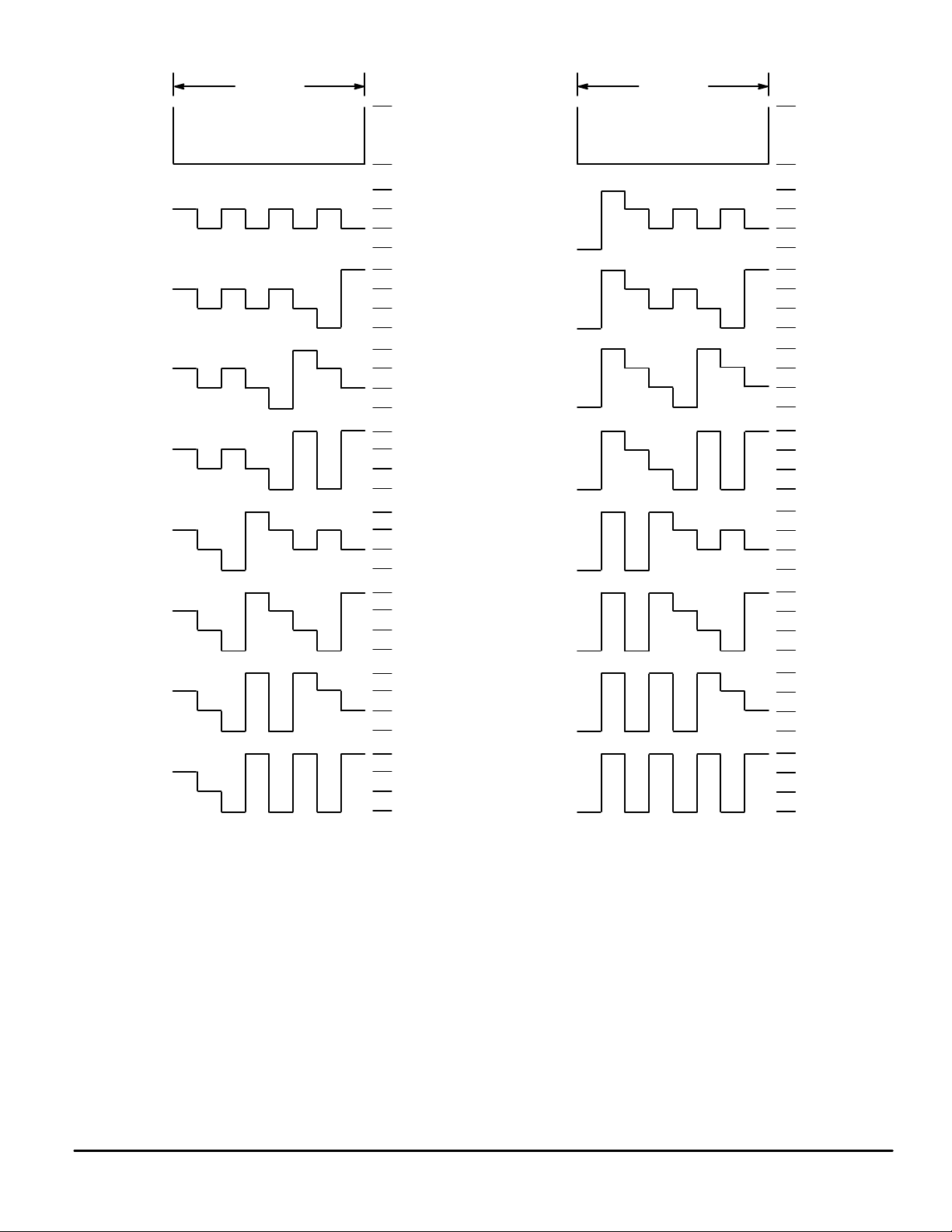
Figure 4 shows the sequence of backplanes. Figure 5
shows the possible configurations of the frontplanes relative
to the backplanes. When a backplane driver is on, its output
switches from V
FRAME
SYNC
PULSE
to 0 V , and when it is off, it switches from
LCD
TIME FRAME
1/3 V
output switches from 0 V to V
from 2/3 V
LCD
to 2/3 V
to 1/3 V
LCD
. When a frontplane driver is on, its
LCD
LCD
, and when it is off, it switches
LCD
.
The LCD drive and timing section provides the multiplex signals and backplane driver input signals and formats the frontplane and backplane waveforms. It also provides a “frame
sync” pulse which may be used in a system where many LCD
drivers are cascaded, to synchronize the backplanes/frontplanes of all participating LCD drivers.
The address pins are used in cascaded systems to uniquely
distinguish one LCD driver from another (and from any other
chips on the same bus) and to define one LCD driver as the
“master” in the system. There must be one master in any
system.
The enable pin may be used as a third control line in the
communication bus. It may be used to define the moment
when the data is latched. If not used, then the data is latched
after 128 bits of data have been received.
V
LCD
0 V
BP1
BP2
BP3
BP4
Figure 4. Backplane Sequence
V
LCD
2/3 (V
1/3 (V
0 V
V
LCD
2/3 (V
1/3 (V
0 V
V
LCD
2/3 (V
1/3 (V
0 V
V
LCD
2/3 (V
1/3 (V
0 V
LCD
LCD
LCD
LCD
LCD
LCD
LCD
LCD
)
)
)
)
)
)
)
)
MC145003 • MC145004 MOTOROLA
4
FRAME
SYNC
PULSE
TIME FRAME
V
0 V
LCD
FRAME
SYNC
PULSE
TIME FRAME
V
0 V
LCD
FP DATA
BITS
4321
0000
1000
0100
1100
0010
1010
0110
1110
V
LCD
2/3 (V
1/3 (V
0 V
V
LCD
2/3 (V
1/3 (V
0 V
V
LCD
2/3 (V
1/3 (V
0 V
V
LCD
2/3 (V
1/3 (V
0 V
V
LCD
2/3 (V
1/3 (V
0 V
V
LCD
2/3 (V
1/3 (V
0 V
V
LCD
2/3 (V
1/3 (V
0 V
V
LCD
2/3 (V
1/3 (V
0 V
LCD
LCD
LCD
LCD
LCD
LCD
LCD
LCD
LCD
LCD
LCD
LCD
LCD
LCD
LCD
LCD
V
)
)
)
)
)
)
)
)
)
)
)
)
)
)
)
)
FP DATA
BITS
4321
0001
1001
0101
1101
0011
1011
0111
1111
LCD
2/3 (V
1/3 (V
0 V
V
LCD
2/3 (V
1/3 (V
0 V
V
LCD
2/3 (V
1/3 (V
0 V
V
LCD
2/3 (V
1/3 (V
0 V
V
LCD
2/3 (V
1/3 (V
0 V
V
LCD
2/3 (V
1/3 (V
0 V
V
LCD
2/3 (V
1/3 (V
0 V
V
LCD
2/3 (V
1/3 (V
0 V
LCD
LCD
LCD
LCD
LCD
LCD
LCD
LCD
LCD
LCD
LCD
LCD
LCD
LCD
LCD
LCD
)
)
)
)
)
)
)
)
)
)
)
)
)
)
)
)
MOTOROLA
Figure 5. Frontplane Combinations
MC145003 • MC145004
5
 Loading...