Motorola MC14499DW, MC14499P Datasheet

MC14499MOTOROLA
1
" !%
#
$" "
CMOS
The MC14499 is a 7–segment alphanumeric LED decoder/driver with a serial
interface port to provide communication with CMOS microprocessors and
microcomputers. T his d evice f eatures NPN output drivers which a llow
interfacing to common cathode LED displays through external series resistors.
• High–Current Segment Drivers On–Chip
• CMOS MPU compatible Input Levels
• Wide Operating Voltage Range: 4.5 to 6.5 V
• Operating Temperature Range: 0 to 70°C
• Drives Four Characters with Decimal Points
• Also See MC14489
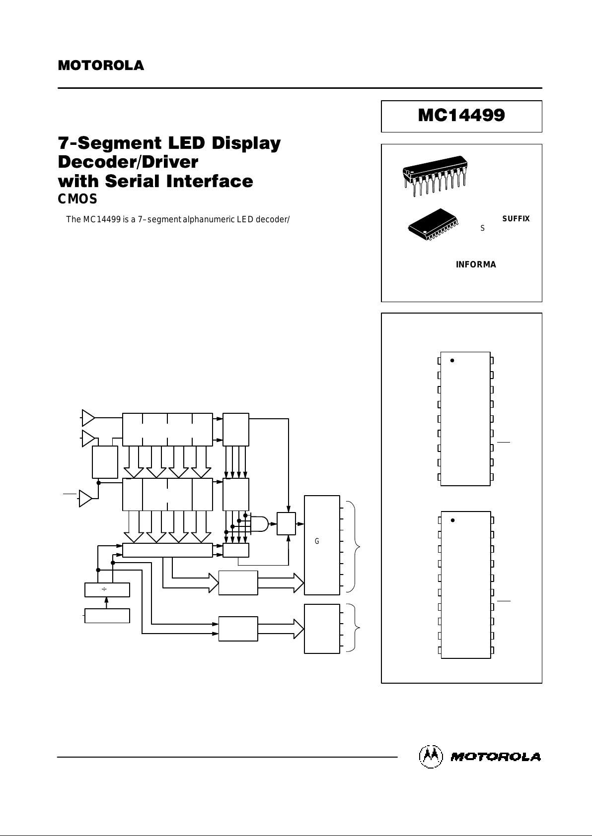
16–BIT SHIFT REGISTER
BLOCK DIAGRAM
CLK
ENB
DATA
OSC
B 4
MULTIPLEXER
2:1
MUX
SEGMENT
DECODER
DECODER
SCANNER
BUFFERS
SEGMENT
DRIVERS
4 BITS
D
20
C
Q
5
C
44 4 4
4
4
A B
7
DECIMAL
POINT
*Transparent Latch
LATCH
44 4 4
Q1D
4
C
LATCH
C
OSCILLATOR
MUX
h
g
f
e
d
c
b
a
I
II
III
IV
SEGMENT
OUTPUTS
CHARACTER
SELECTORS
4 BITS
QD
C*
Order this document
by MC14499/D
SEMICONDUCTOR TECHNICAL DATA
P SUFFIX
PLASTIC DIP
CASE 707
DW SUFFIX
SOG PACKAGE
CASE 751D
ORDERING INFORMATION
MC14499P Plastic DIP
MC14499DW SOG Package
PIN ASSIGNMENTS
PLASTIC DIP
DATA
b
c
d
V
SS
III
IV
OSC
a g
f
e
V
DD
II
I
ENB
CLK
h
14
15
16
17
18
10
11
12
13
5
4
3
2
1
9
8
7
6
NC
5
4
3
2
1
10
9
8
7
6
14
15
16
17
18
19
20
11
12
13
SOG PACKAGE
NC
c
d
DATA
b
V
SS
III
IV
OSC
a
g
f
e
V
DD
II
I
ENB
CLK
h
18
1
NC = NO CONNECTION
20
1
Motorola, Inc. 1995
SAME AS IN DL130/D R1

MC14499 MOTOROLA
2
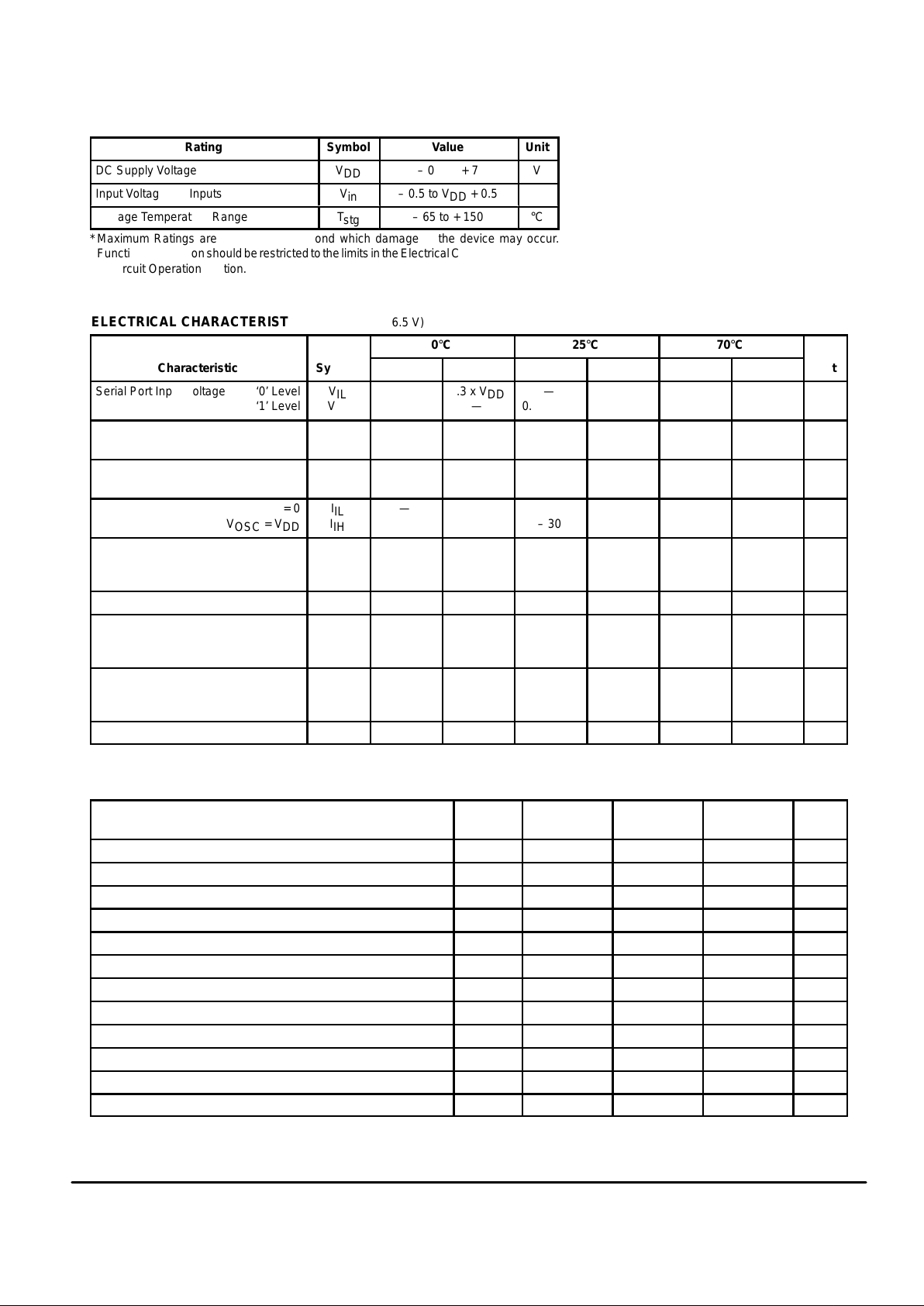
MAXIMUM RATINGS* (Voltages referenced to V
SS
)
Rating
Symbol
Value
Unit
DC Supply Voltage
V
DD
– 0.5 to + 7
V
Input Voltage, All Inputs
V
in
– 0.5 to VDD + 0.5
V
Storage Temperature Range
T
stg
– 65 to + 150
°C
*Maximum Ratings are those values beyond which damage to the device may occur.
Functional operation should be restricted to the limits in the Electrical Characteristics table
or Circuit Operation section.
ELECTRICAL CHARACTERISTICS (V
DD
= 4.5 to 6.5 V)
0°C 25°C 70°C
Characteristic
Symbol
Min Max Min Max Min Max
Unit
Serial Port Input Voltage ‘0’ Level
‘1’ Level
V
IL
V
IH
—
0.7 x V
DD
0.3 x V
DD
—
—
0.7 x V
DD
0.3 x V
DD
—
—
0.7 x V
DD
0.3 x V
DD
—
V
Serial Port Input Current
(Vin = 0 to VDD)
I
in
— ± 0.1 — ± 0.1 — ± 1.0 µA
Oscillator Input Voltage ‘0’ Level
‘1’ Level
V
IL
V
IH
—
0.75 x V
DD
0.25 x V
DD
—
—
0.75 x V
DD
0.25 x V
DD
—
—
0.8 x V
DD
0.2 x V
DD
—
V
Oscillator Input Current V
OSC
= 0
V
OSC
= V
DD
I
IL
I
IH
—
—
100
– 100
30
– 30
80
– 80
10
– 10
—
—
µA
Segment Driver Voltage Below V
DD
I
out
= 50 mA
I
out
= 10 mA
∆V
OH
—
—
1.1
0.8
—
—
1.0
0.75
—
—
1.1
0.8
V
Segment Driver Off Leakage V
out
= 0 I
OZ
— 100 — 50 — 100 µA
Digit Drivers
Source (On) V
out
= 0.8 V
Sink (Off) V
out
= 0.5 V
I
OH
I
OL
6
– 0.2
—
—
5.5
– 0.2
—
—
4
– 0.1
—
—
mA
Supply Current
Vin = 0, I
out
= 0,
C
OSC
= 0.015 µF
I
DD
— 1 — 1 — 1 mA
Maximum Power Dissipation P
D
— 500 — 500 — 500 mW
SWITCHING CHARACTERISTICS (V
DD
= 5 V ± 10%, TA = 0 to 70°C)
Characteristic
Figure
No.
Symbol Min Max Unit
Clock High Time 2 t
CH
2 — µs
Clock Low Time 2 t
CL
2 — µs
Clock Rise Time 2 t
CR
— 2 µs
Clock Fall Time 2 t
CF
— 2 µs
Enable Lead Time 2 tE
LEAD
200 — ns
Enable Lag Time 2 tE
LAG
200 — ns
Data Set–Up Time 2 tD
SUP
200 — ns
Data Hold Time 2 tD
HOLD
1 — µs
Scanner Frequency* 4 1/t
SCAN
50 300 Hz
OSC/Digit Lead Time 4 t
OD
— 10 µs
OSC/Segment Lead Time 4 t
OS
— 10 µs
Digit Overlap 4 t
OV
— 5 µs
*Scanner Capacitance = 0.022 µF.
This device contains circuitry to protect the
inputs against damage due to high static
voltages or electric fields; however, it is advised that normal precautions be taken to avoid
application of any voltage higher than maximum rated voltages to this high impedance
circuit. For proper operation, it is recommended that Vin and V
out
be constrained to
the range VSS ≤ (Vin or V
out
) ≤VDD.

MC14499MOTOROLA
3
CIRCUIT OPERATION
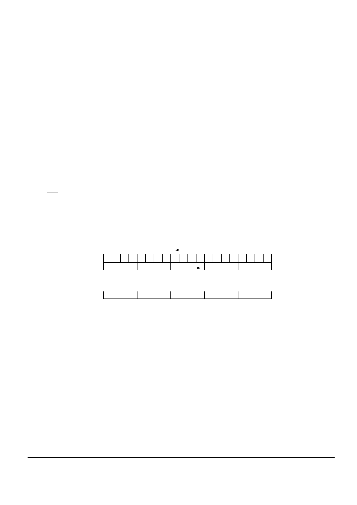
The circuit accepts a 20–bit input, 16 bits for the four–digit
display plus 4 bits for the decimal point — these latter four
bits are optional.
The input sequence is the decimal point code followed by
the four digits, as shown in Figure 1.
In order to enter data the enable input, ENB
, must be active low. The sample and shift are accomplished on the falling clock edge, see Figure 2. Data are loaded from the shift
register to the latches when ENB
goes high. While the shift
register is being loaded, the previous data are stored in the
latches.
If the decimal point is used, the system requires 20 clock
pulses to load data; otherwise only 16 are required.
CASCADING
The circuit may be cascaded in the following manner.
If a 1111 word is loaded into the decimal point latch, the
output of the shift register is switched to the decimal point
driver, see Figure 3. Therefore, to cascade n four–digit display drivers, a set–up is used which loads the 1111 cascading word:
1. ENB
= active low.
2. Load 20 bits, the first four bits being 1, with 20 clock
pulses.
3. ENB
= high, to load the latch.
4. Repeat steps 1 to 3 (n – 1) times.
5. (n x 20) bits can be loaded into n circuits, with 1111 as
decimal point word to continue the cascading.
SCANNER
The scanner frequency is determined by an on–chip oscillator, which requires an external frequency–determining capacitor. The capacitor v oltage varies between two trigger
levels at the oscillator frequency.
An external oscillator signal can be used, within the recommended operating range of 200 to 800 Hz. For test purposes
this frequency may be increased up to 10 kHz.
A divide by four counter provides four non–overlapping
scanner waveforms corresponding to the four digits — see
Figure 4.
SEGMENT DECODER
The code used in these matrix decoders is shown in Figure 5.
OUTPUT DRIVERS
There are two different drivers:
• The segment and decimal point drivers; these are NPN
emitter followers with no current limiting devices.
• The digit output buffers; these are short–circuit protected
CMOS devices.
A typical application circuit is shown in Figure 6.
Figure 1. Input Sequence
18 17 16 15 14 13 12 11 10 9 8 7 6 5 41920 3 2 1
TIME
SHIFT
BIT NO.
DIGIT IV DIGIT III DIGIT II DIGIT I DECIMAL POINT
MSB
LSB
MSB
LSB
MSB
DIGIT IV
DIGIT III
DIGIT II
DIGIT I
MSB
LSB
LSB
 Loading...