

MC14489MOTOROLA
1
CMOS
The MC14489 is a f lexible l ight–emitting–diode d river which d irectly
interfaces to individual lamps, 7–segment displays, or various combinations of
both. LEDs wired with common cathodes are driven in a multiplexed–by–5
fashion. Communication with an MCU/MPU is established through a synchronous serial port. The MC14489 features data retention plus decode and scan
circuitry, thus relieving processor overhead. A single, current–setting resistor is
the only ancillary component required.
A single device can drive any one of the following: a 5–digit display plus
decimals, a 4–1/2–digit display plus decimals and sign, or 25 lamps. A special
technique allows driving 5 1/2 digits; see Figure 16. A configuration register
allows t he drive capability t o be partitioned off t o suit many a dditional
applications. The on–chip decoder outputs 7–segment–format numerals 0 to 9,
hexadecimal characters A to F, plus 15 letters and symbols.
The MC14489 is compatible with the Motorola SPI and National MICROWIRE serial data ports. The chip’s patented BitGrabber registers augment
the serial interface by allowing random access without steering or address bits.
A 24–bit transfer updates the display register. Changing the configuration
register requires an 8–bit transfer.
• Operating Voltage Range of Drive Circuitry: 4.5 to 6 V
• Operating Junction Temperature Range: – 40° to 130°C
• Current Sources Controlled by Single Resistor Provide Anode Drive
• Low–Resistance FET Switches Provide Direct Common Cathode Interface
• Low–Power Mode (Extinguishes the LEDs) and Brightness Controlled via
Serial Port
• Special Circuitry Minimizes EMI when Display is Driven and Eliminates
EMI in Low–Power Mode
• Power–On Reset (POR) Blanks the Display on Power–Up, Independent of
Supply Ramp Up Time
• May Be Used with Double–Heterojunction LEDs for Optimum Efficiency
• Chip Complexity: 4300 Elements (FETs, Resistors, Capacitors, etc.)
• See Application Note AN431,
Temperature Measurement and Display
Using the MC68HC05B4 and the MC14489
and Engineering Bulletin
EB153,
Driving a Seven–Segment Display with the N
EURON
C
HIP
BitGrabber is a trademark of Motorola Inc.
MICROWIRE is a trademark of National Semiconductor Corp.
Order this document
by MC14489/D
SEMICONDUCTOR TECHNICAL DATA
PIN ASSIGNMENT
P SUFFIX
PLASTIC DIP
CASE 738
DW SUFFIX
SOG PACKAGE
CASE 751D
ORDERING INFORMATION
MC14489P Plastic DIP
MC14489DW SOG Package
b
d
V
DD
e
f
ENABLE
BANK 1
Rx
a
c 5
4
3
2
1
10
9
8
7
6
14
15
16
17
18
19
20
11
12
13
BANK 4
BANK 5
DATA OUT
h
g
CLOCK
DATA IN
BANK 2
V
SS
BANK 3
20
1
20
1
Motorola, Inc. 1995
REV 3
10/95
MC14489 MOTOROLA
2
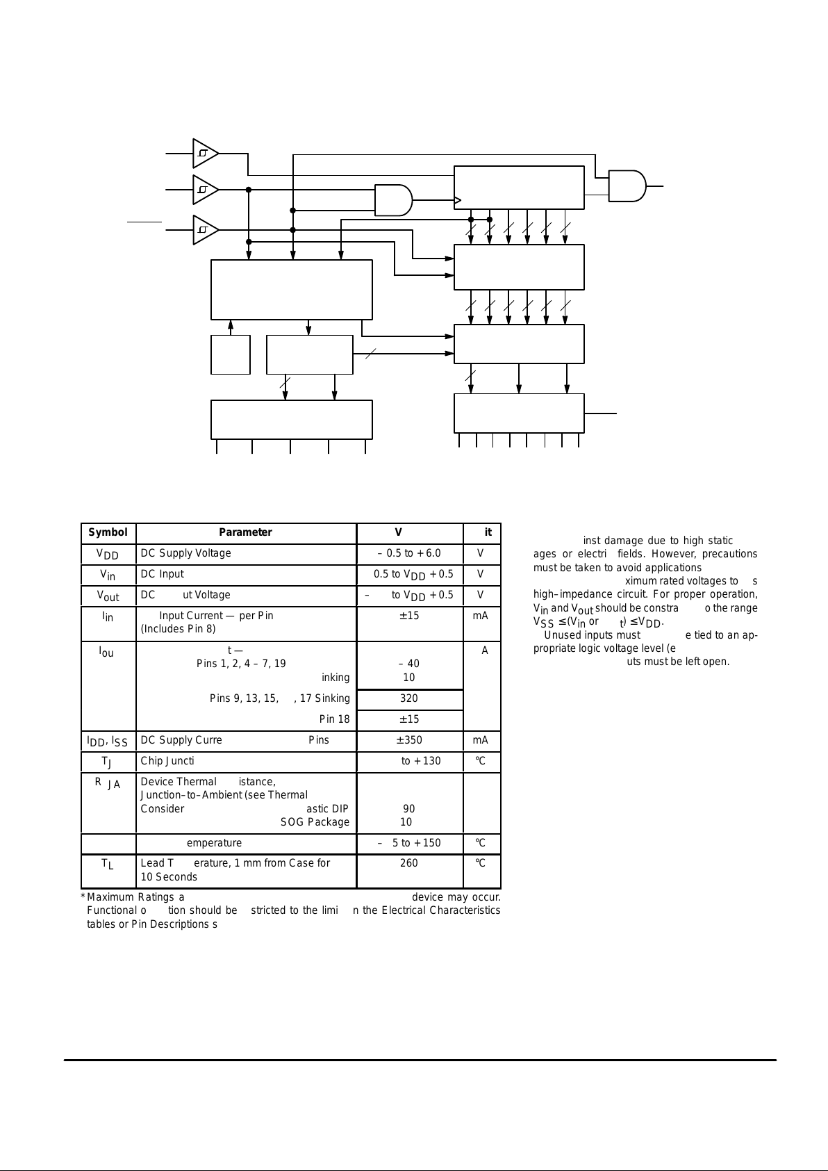
BLOCK DIAGRAM
1
BitGrabber
CONFIGURATION REGISTER
8 BITS
Rx
DATA OUT
8
2 20
12
BitGrabber
DISPLAY REGISTER
24 BITS
NIBBLE MUX AND
DECODER ROM
ANODE DRIVERS
(CURRENT SOURCES)
BANK SWITCHES (FETs)
194567
a b
DATA IN
c d e f g h
24–1/2–STAGE
SHIFT REGISTER
11
10
7
4
444
44
4
44444
18
POR
9 13 15 16 17
5
5
CLOCK
ENABLE
OSCILLATOR AND
CONTROL LOGIC
BANK 1 BANK 2 BANK 3 BANK 4 BANK 5
PIN 3 = V
DD
PIN 14 = V
SS
h DIM/BRIGHT
BLANK
a TO g
D
C
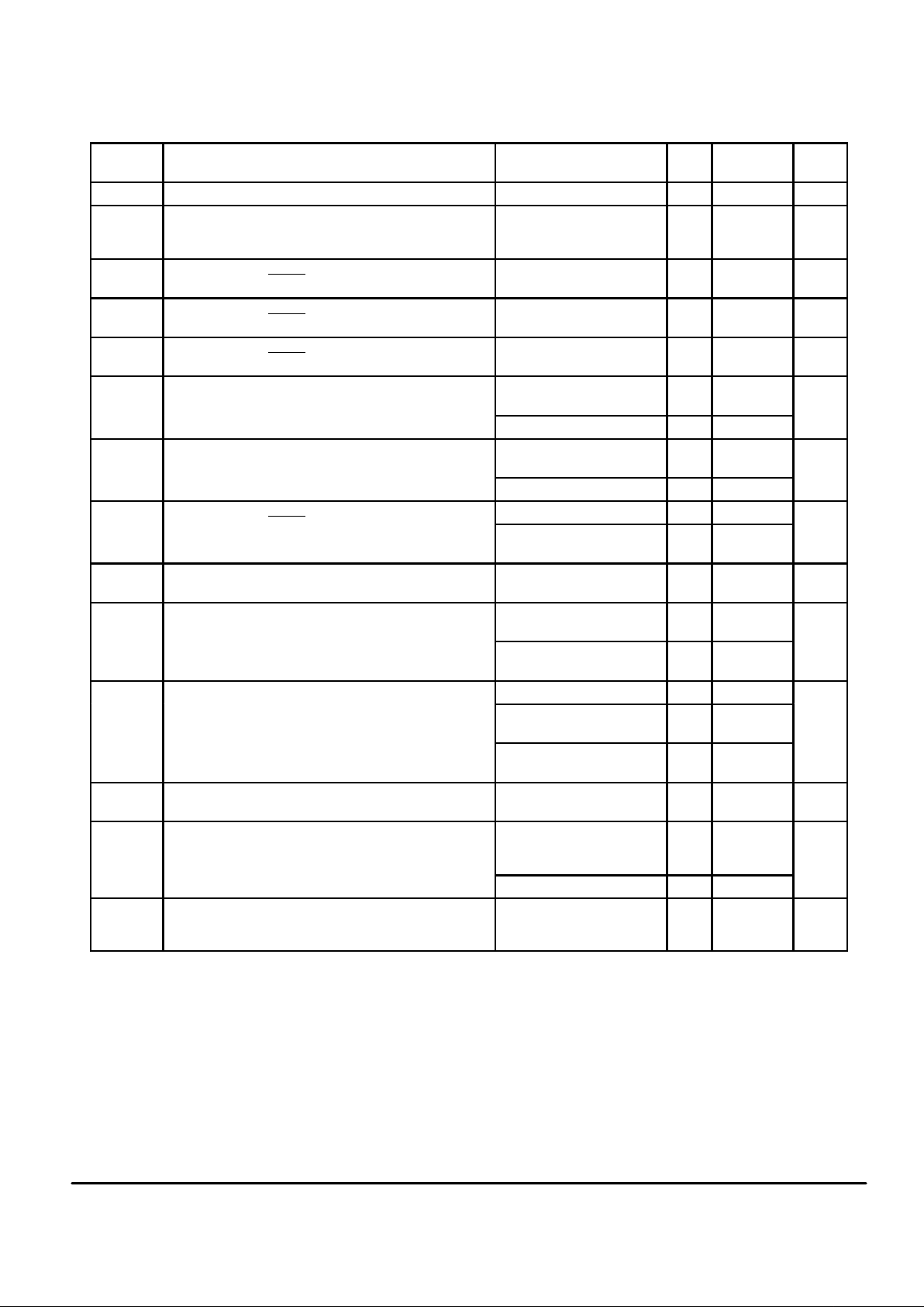
MAXIMUM RATINGS* (Voltages Referenced to V
SS
)
Symbol
Parameter
Value
Unit
V
DD
DC Supply Voltage
– 0.5 to + 6.0
V
V
in
DC Input Voltage
– 0.5 to VDD + 0.5
V
V
out
DC Output Voltage
– 0.5 to VDD + 0.5
V
I
in
DC Input Current — per Pin
(Includes Pin 8)
± 15
mA
I
out
DC Output Current —
Pins 1, 2, 4 – 7, 19, 20 Sourcing
Sinking
– 40
10
mA
Pins 9, 13, 15, 16, 17 Sinking
320
Pin 18
± 15
IDD, ISSDC Supply Current, VDD and VSS Pins
± 350
mA
T
J
Chip Junction Temperature
– 40 to + 130
°C
R
θJA
Device Thermal Resistance,
Junction–to–Ambient (see Thermal
Considerations section) Plastic DIP
SOG Package
90
100
°C/W
T
stg
Storage Temperature
– 65 to + 150
°C
T
L
Lead Temperature, 1 mm from Case for
10 Seconds
260
°C
*Maximum Ratings are those values beyond which damage to the device may occur.
Functional operation should be restricted to the limits in the Electrical Characteristics
tables or Pin Descriptions section.
This device contains protection circuitry to
guard against damage due to high static voltages or electric fields. However, precautions
must be taken to avoid applications of any voltage higher than maximum rated voltages to this
high–impedance circuit. For proper operation,
Vin and V
out
should be constrained to the range
VSS ≤ (Vin or V
out
) ≤ VDD.
Unused inputs must always be tied to an appropriate logic voltage level (e.g., either VSS or
VDD). Unused outputs must be left open.
MC14489MOTOROLA
3
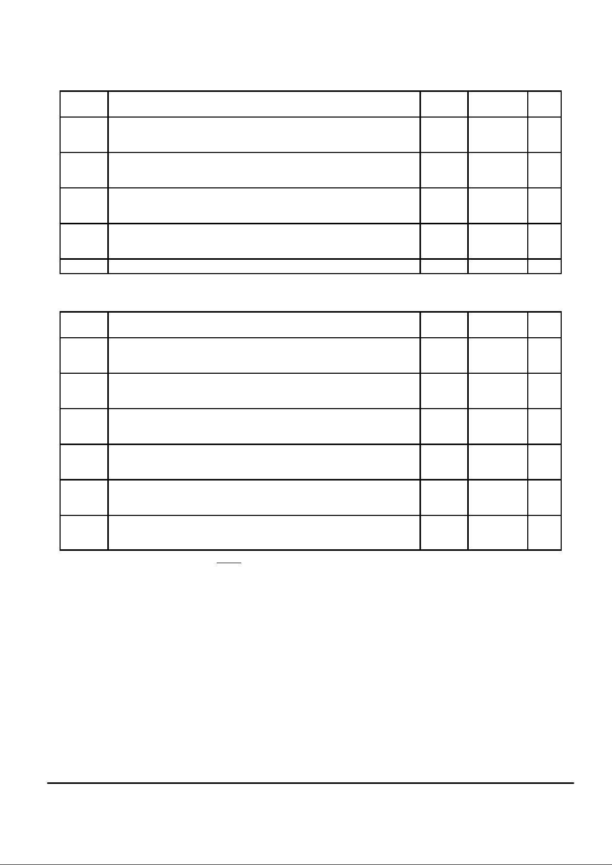
ELECTRICAL CHARACTERISTICS (Voltages Referenced to V
SS
, TJ = – 40° to 130°C* unless otherwise indicated)
Symbol
Parameter Test Condition
V
DD
V
Guaranteed
Limit
Unit
V
DD
Power Supply Voltage Range of LED Drive Circuitry — 4.5 to 6.0 V
VDD (stby) Minimum Standby Voltage Bits Retained in Display and
Configuration Registers, Data
Port Fully Functional
— 3.0 V
V
IL
Maximum Low–Level Input Voltage
(Data In, Clock, Enable
)
3.0
6.0
0.9
1.8
V
V
IH
Minimum High–Level Input Voltage
(Data In, Clock, Enable
)
3.0
6.0
2.1
4.2
V
V
Hys
Minimum Hysteresis Voltage
(Data In, Clock, Enable
)
3.0
6.0
0.2
0.4
V
V
OL
Maximum Low–Level Output Voltage
(Data Out)
I
out
= 20 µA 3.0
6.0
0.1
0.1
V
I
out
= 1.3 mA 4.5 0.4
V
OH
Minimum High–Level Output Voltage
(Data Out)
I
out
= – 20 µA 3.0
6.0
2.9
5.9
V
I
out
= – 800 µA 4.5 4.1
I
in
Maximum Input Leakage Current
Vin = VDD or V
SS
6.0 ± 2.0
µA
(Data In, Clock, Enable)
Vin = VDD or VSS,
TJ = 25°C only
6.0 ± 0.1
i
OL
Minimum Sinking Current
(a, b, c, d, e, f, g, h)
V
out
= 1.0 V 4.5 0.2 mA
i
OH
Peak Sourcing Current — See Figure 9 for currents up to
35 mA (a, b, c, d, e, f, g, h)
Rx = 2.0 kΩ, V
out
= 3.0 V,
Dimmer Bit = High
5.0 13 to 17.5
mA
Rx = 2.0 kΩ, V
out
= 3.0 V,
Dimmer Bit = Low
5.0 6 to 9
I
OZ
Maximum Output Leakage Current
V
out
= VDD (FET Leakage) 6.0 50
µA
(Bank 1, Bank 2, Bank 3, Bank 4, Bank 5)
V
out
= VDD (FET Leakage),
TJ = 25°C only
6.0 1
V
out
= VSS (Protection Diode
Leakage)
6.0 1
R
on
Maximum ON Resistance
(Bank 1, Bank 2, Bank 3, Bank 4, Bank 5)
I
out
= 0 to 200 mA 5.0 10 Ω
IDD, I
SS
Maximum Quiescent Supply Current
Device in Low–Power Mode,
Vin = VSS or VDD, Rx in
Place, Outputs Open
6.0 100
µA
Same as Above, TJ = 25°C 6.0 20
I
ss
Maximum RMS Operating Supply Current
(The VSS leg does not contain the Rx current component.
See Pin Descriptions.)
Device NOT in Low–Power
Mode, Vin = VSS or VDD,
Outputs Open
6.0 1.5 mA
*See Thermal Considerations section.
MC14489 MOTOROLA
4
AC ELECTRICAL CHARACTERISTICS (T
J
= – 40° to 130°C*, CL = 50 pF, Input tr = tf = 10 ns)
Symbol
Parameter
V
DD
V
Guaranteed
Limit
Unit
f
clk
Serial Data Clock Frequency, Single Device or Cascaded Devices
NOTE: Refer to Clock tw below
(Figure 1)
3.0
4.5
6.0
dc to 3.0
dc to 4.0
dc to 4.0
MHz
t
PLH
,
t
PHL
Maximum Propagation Delay, Clock to Data Out
(Figures 1 and 5)
3.0
4.5
6.0
140
80
80
ns
t
TLH
,
t
THL
Maximum Output Transistion Time, Data Out
(Figures 1 and 5)
3.0
4.5
6.0
70
50
50
ns
f
R
Refresh Rate — Bank 1 through Bank 5
(Figures 2 and 6)
3.0
4.5
6.0
NA
700 to 1900
700 to 1900
Hz
C
in
Maximum Input Capacitance — Data In, Clock, Enable — 10 pF
*See Thermal Considerations section.
TIMING REQUIREMENTS (T
J
= – 40° to 130°C*, Input tr = tf = 10 ns unless otherwise indicated)
Symbol Parameter
V
DD
V
Guaranteed
Limit
Unit
tsu, t
h
Minimum Setup and Hold Times, Data In versus Clock
(Figure 3)
3.0
4.5
6.0
50
40
40
ns
tsu, th,
t
rec
Minimum Setup, Hold, ** and Recovery Times, Enable versus Clock
(Figure 4)
3.0
4.5
6.0
150
100
100
ns
t
w(L)
Minimum Active–Low Pulse Width, Enable
(Figure 4)
3.0
4.5
6.0
4.5
3.4
3.4
µs
t
w(H)
Minimum Inactive–High Pulse Width, Enable
(Figure 4)
3.0
4.5
6.0
300
150
150
ns
t
w
Minimum Pulse Width, Clock
(Figure 1)
3.0
4.5
6.0
167
125
125
ns
tr, t
f
Maximum Input Rise and Fall Times — Data In, Clock, Enable
(Figure 1)
3.0
4.5
6.0
1
1
1
ms
*See Thermal Considerations section.
**For a high–speed 8–Clock access, th for Enable
is determined as follows:
VDD = 3 to 4.5 V, f
clk
> 1.78 MHz: th = 4350 – (7500/f
clk
)
VDD = 4.5 to 6 V, f
clk
> 2.34 MHz: th = 3300 – (7500/f
clk
)
where th is in ns and f
clk
is in MHz.
NOTES:
1. This restriction does NOT apply for f
clk
rates less than those listed above. For “slow” f
clk
rates, use the th limits in the above table.
2. This restriction does NOT apply for an access involving more than 8 Clocks. For > 8 Clocks, use the th limits in the above table.
MC14489MOTOROLA
5
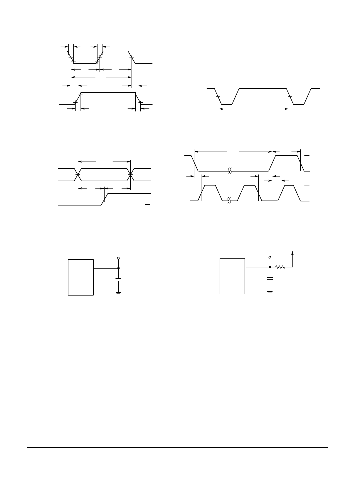
Figure 1. Figure 2.
10%
V
DD
1/f
clk
DATA OUT
CLOCK
90%
50%
90%
50%
10%
t
PLH
t
PHL
t
TLH
t
THL
t
w
t
w
t
f
t
r
BANK
OUTPUT
50%
1/f
R
V
SS
Figure 3. Figure 4.
D
ATA IN
CLOCK
50%
VALID
50%
t
su
t
h
V
DD
V
DD
CLOCK
ENABLE
50%
t
su
t
h
FIRST
CLOCK
LAST
CLOCK
t
rec
50%
V
DD
V
DD
tw(H)
tw(L)
V
SS
V
SS
V
SS
V
SS
Figure 5. Figure 6.
TEST POINT
DEVICE
UNDER
TEST
C
L
*
*Includes all probe and fixture capacitance.
TEST POINT
DEVICE
UNDER
TEST
C
L
*
*Includes all probe and fixture capacitance.
V
DD
56
Ω

MC14489 MOTOROLA
6
PIN DESCRIPTIONS
DIGITAL INTERFACE
Data In (Pin 12)
Serial Data Input. The bit stream begins with the MSB and
is shifted in on the low–to–high transition of Clock. When the
device is not cascaded, the bit pattern is either 1 byte (8 bits)
long to change the configuration register or 3 bytes (24 bits)
long to update the display register. For two chips cascaded,
the pattern is either 4 or 6 bytes, respectively. The display
does not change during shifting (until Enable
makes a low–
to–high transition) which allows slow serial data rates, if desired.
The bit stream needs neither address nor steering bits due
to the innovative BitGrabber registers. Therefore, all bits in
the stream are available to be data for the two registers. Random access of either register is provided. That is, the registers may be accessed in any sequence. Data is retained in
the registers over a supply range of 3 to 6 V. The format is
shown in Figures 7 and 8. Information on the segment decoder is given in Table 1.
Data In typically switches near 50% of VDD and has a
Schmitt–triggered input buffer. These features combine to
maximize noise immunity for use in harsh environments and
bus applications. T his input can b e directly interfaced to
CMOS devices with outputs guaranteed to switch near rail–
to–rail. When interfacing to NMOS or TTL devices, either a
level shifter (MC14504B, MC74HCT04A) or pullup resistor of
1 kΩ to 10 kΩ must be used. Parameters to be considered
when sizing the resistor are the worst–case IOL of the driving
device, maximum tolerable power consumption, and maximum data rate.
Clock (Pin 11)
Serial Data Clock Input. Low–to–high transitions on Clock
shift bits available at Data In, while high–to–low transitions
shift bits from Data Out. The chip’s 24–1/2–stage shift register is static, allowing clock rates down to dc in a continuous
or intermittent mode. The Clock input does not need to be
synchronous with the on–chip clock oscillator which drives
the multiplexing circuit.
Eight clock cycles are required to access the configuration
register, while 24 are needed for the display register when
the MC14489 is not cascaded. See Figures 7 and 10.
As shown in Figure 11, two devices may be cascaded. In
this case, 32 clock cycles access the configuration register
and 48 access the display register, as depicted in Figure 8.
Cascading of 3, 4, and 5 devices is shown in Figures 12,
13, and 14, respectively.
Clock typically switches near 50% o f VDD and h as a
Schmitt–triggered input buffer. Slow Clock rise and fall times
are tolerated. See the last paragraph of Data In for more information.
NOTE
To guarantee proper operation of the power–on
reset (POR) circuit, the Clock pin must NOT be
floated or toggled during power–up. That is, the
Clock pin m ust b e stable until the VDD pin
reaches at least 3 V.
If control of the Clock pin during power–up is not
practical, then the MC14489 must be reset via bit
C0 in the C register. To accomplish this, C0 is reset low, then set high.
Enable
(Pin 10)
Active–Low Enable Input. This pin allows the MC14489 to
be used on a serial bus, sharing Data In and Clock with other
peripherals. When Enable
is in an inactive high state, Data
Out is forced to a known (low) state, shifting is inhibited, and
the port is held in the initialized state. To transfer data to the
device, Enable
(which initially must be inactive high) is taken
low, a serial transfer is made via Data In and Clock, and
Enable is taken high. The low–to–high transition on Enable
transfers data to either the configuration or display register,
depending on the data stream length.
Every rising edge on Enable initiates a blanking interval
while data is loaded. Thus, continually loading the device
with the same data may cause the LEDs on some banks to
appear dimmer than others.
NOTE
Transitions on Enable
must not be attempted
while Clock is high. This puts the device out of
synchronization with the microcontroller. Resynchronization occurs when Enable
is high a nd
Clock is low.
This input is also Schmitt–triggered and switches near
50% of VDD, thereby minimizing the chance of loading erroneous data in the registers. See the last paragraph of Data In
for more information.
Data Out (Pin 18)
Serial Data Output. Data is transferred out of the shift register through Data Out on the high–to–low transition of Clock.
This output is a no connect, unless used in one of the manners discussed below.
When cascading MC14489’s, Data Out feeds Data In of
the next device per Figures 11, 12, 13, and 14.
Data Out could be fed back to an MCU/MPU to perform a
wrap–around test of serial data. This could be part of a system check conducted at power–up to test the integrity of the
system’s processor, pc board traces, solder joints, etc.
The pin could be monitored at an in–line Q.A. test during
board manufacturing.
Finally, Data Out facilitates troubleshooting a system.
DISPLAY INTERFACE
Rx (Pin 8)
External Current–Setting Resistor. A resistor tied between
this pin and ground (VSS) determines the peak segment drive
current delivered at pins a through h. Pin 8’s resistor ties into
a current mirror with an approximate current gain of 10 when
bit D23 = high (brighten). With D23 = low, the peak current is
reduced about 50%. Values for Rx range from 700 Ω to infin-
ity. When Rx = ∞ (open circuit), the display is extinguished.
For proper current control, resistors having ± 1% tolerance
should be used. See Figure 9.
CAUTION
Small Rx values may cause the chip to overheat
if precautions are not observed. See Thermal
Considerations.
 Loading...