

Motorola MC14419L, MC14419P Datasheet
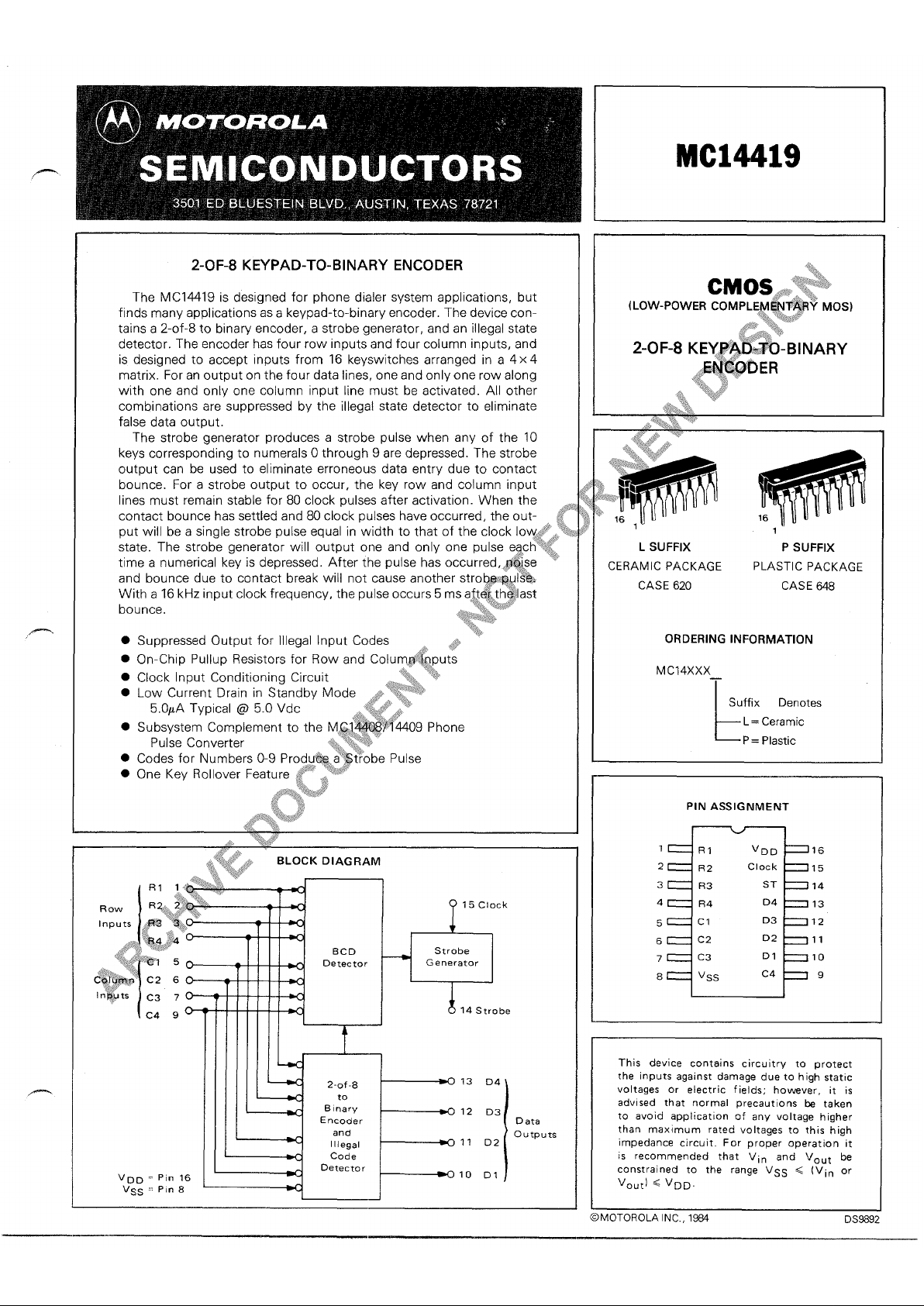
2-OF-8 KEYPAD-TO-BINARY ENCODER
The MC14419 is designed for phone dialer system applications, but
finds many applications as a keypad-to-binary encoder. The device contains a 2-of-8 to binary encoder, a strobe generator, and an illegal state
detector. The encoder has four row inputs and four column inputs, and
is designed to accept inputs from 16 keyswitches arranged in a 4x 4
matrix. For an output on the four data lines, one and only one row along
with one and only one column input line must be activated. All other
combinations are suppressed by the illegal state detector to eliminate
false data output.
The strobe generator produces a strobe pulse when any of the 10
keys corresponding to numerals O through 9 are depressed. The strobe
output can be used to eliminate erroneous data entry due to contact
bounce. For a strobe output to occur, the key row and column input
lines must remain stable for 80 clock pulses after activation. When the
*,,}tt
contact bounce has settled and 80 clock pulses have occurred, the out- t’
put will be a single strobe pulse equal in width to that of the clock low.#}’ $!
state. The strobe generator will output one and only one pulse eq,ch j,<
.<~>,,,,\,..?
time a numerical key is depressed. After the pulse has occurred,,$x+se ““
and bounce due to contact break will not cause another stro@#iQQ15&.
With a 16 kHz input clock frequency, the pulse
occurs 5 ms a~t~~th,$last
bounce.
.++\,%,‘./\\.
)~~<.?,!F,::’k:+>
‘!%.
‘i\}.
. Suppressed Output for Illegal Input Codes
>f,i$
,>.>
MCl~19
L SUFFIX
P SUFFIX
CERAMIC PACKAGE PLASTIC PACKAGE
CASE 620
CASE W
ORDERING INFORMATION
MC14XXX
—
L
suffix Denotes
L= Ceramic
P= Plastic
PIN ASSIGNMENT
1
n
RI
v~~
16
2
R2
Clock
15
3
R3
ST
14
4
R4
D4
13
5
cl
D3
12
6
C2
02
11
7
C3
D1
10
8
Vss
C4
9
This device contains circuitry to protect
the inputs against damage due to high
static
voltages or electric fields; howver, it is
advised that normal precautions b taken
to avoid application of anv voltage higher
than maximum rated voltages to this high
impedance circuit. For proper operation it
IS
recommended that Vin and Vout be
constrained to the range VSS < (Vin or
Vout) < VDD.
MOTOROLA INC , lW
DS9892
—
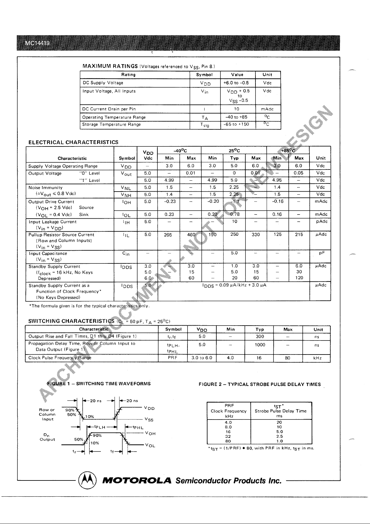
MAXIMUM RATINGS (Voltages referenced to VSS, Pin 8.)
Rating
Symbol Value
Unit
DC Supply Voltage VDD
+6.0 to -0.5
Vdc
Input Voltage, All Inputs
I
V in VDD t 05
V dc
to
I
Vss
-0.5
II
DC Current Drain per Pin
I
10
mAdc
Operating Temperature Range TA
-40 to +85
‘c
Storage Temperature Range
Tstg
-65 to +1 50 ‘c
ELECTRICAL CHARACTERISTICS
\,,*,. .,.
VDD
40°c 25°C .<<c&fb.’~”
Characteristic
Symbol
Vdc
Min Max
Min
Typ Max
.:&iri”k~r$W Max
Unit
Supply Voltage Operating Range
VDD
—
3.0
6.0
3,0
5.0 6.0,9
,. Fqg
6.0
Vdc
Output Voltage
“O” Level
Vout
5.0 –
0.01
0
o,@#’t. ~ “
‘ ‘i,.::~.i.—
—
0.05
Vdc
“l” Level 5.0
4,99 4.99 5.0
+*.*- ..!.
—
‘,’~t- $;>.\,$s:
4,95
–
Vdc
Noise Immunity
VNL
5.0
1.5 –
1,5
,,!*.,,,,.,.!..
2.25
::,./:.’.*,:,.
1,4 –
Vdc
?.
(AVout <0.8 Vdc)
VNH
5.0
1.4
—
1.5
2 ,J~R ‘*_
1,5
—
Vdc
Output Drive Current
IOH
5.0 -0.23 –
-0.20
,$.y,;f~f’’’”~’‘ –
-0,16
—
mAdc
(VOH = 2.5 Vdc)
Source
<\, t\.
,8.”
,}:
(VOL = 0.4 Vdc)
Sink
!OL
5.0
0.23
—
o ,2g:’:*, “i?~~$8 _
0.16 –
mAdc
Input Leakage Current
IIH
5.0
— —
. —“~t\:
10
— — —
>,,,,, .
pAdc
(Vin = VDD)
,$>~.~:!..
..*.
Pullup Resistor Source Current
IIL 5,0
265
250
330
125
215
pAdc
(Row and Column Inputs)
(Vin = VSS)
Input Capacitance
Cin
— —
.,
5.0 – –
pF
(Vin = VSS)
,:k)
,,t.,
Standby Supply Current
IDDS 3.0 ,>’’?4..
3.0
—
1.0
3.0
—
6,0
pAdc
(fclock = 16 kHz, No Keys
5.0 )+~. J’”
15
—
5.0 15
—
30
.$,)),*X<;+’~.
Depressed)
6.* t~,,’ ‘~
60 –
20 60
—
120
*
Standby SupPlV Current as a
lDDs
~g~:
.,> ‘“
IDDS = 0.09 pA/kHz + 3.0 PA
~Adc
Function of Clock FrequencV*
.(
,~,,,. .<:,.~+,::
(No Keys Depressed)
i\;\&.*?.*,~~
*,/,),
?,$,. *’
●The formula given is for the typical characteri3X~:s~@rilV.
,>,
,h.#.\.~ ~i<.
Character~@&$~*’:
SVmbol
VDD Min
Tvp Max
Unit
Output Rise and Fall Times, Q,f t~~$$#4 (Figure 1)
‘r,tf
5.0
—
300
—
ns
Propagation DelaV Time, Q@$&r~Qolumn Input to
Data Output ( Figure 1%$. ~~~~’
tpLH, 5.0
—
1000
—
ns
,??.> \..
tpHL
Clock Pulse Freque~&~;@#R&
PR F
3.0 to 6.0 4.0
16
80 kHz
.q~)
“~,!e,
“.*>.L,....
,,,,,, $,>,1 ~~
\y,,..~
.),“~~
$.
FIGURE 2 – TYPICAL STROBE PULSE DELAY TIMES
PRF
tST *
Clock Frequencv Strobe Pulse DelaV Time
kH
Z
ms
~
*tST= (l/p RF) ● 80, with PRF in kHz, tST in m$
@
MOTOROLA Semiconductor Products Inc.
 Loading...