MC144112MOTOROLA
1
Advance Information
CMOS
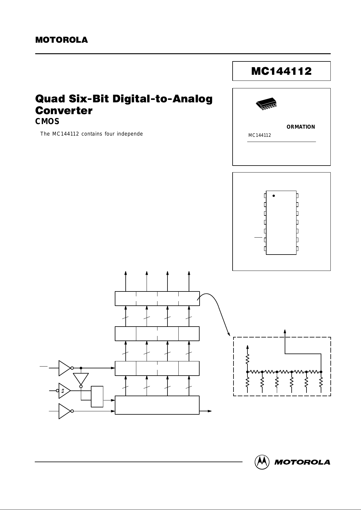
The MC144112 contains four independent DACs which are controlled
through a common serial data port. When all DACs are utilized, there are 24 bits
in the serial data stream. However, if not all DACs are utilized, the bit stream
length may be reduced by up to six bits per unused DAC.
For new designs, the MC144112 is preferred over the MC144110 and
MC144111. The newer MC144112 offers a wider operating temperature range,
lower operating supply voltage, and lower supply current.
• Operating Supply Voltage Range: 2.7 to 5.5 V
*
• Maximum Supply Current (per Package) —
All DAC Outputs = Zero: 1.25 mA @ 2.7 V
2.1 mA @ 4.5 V
All DAC Outputs = Full Scale: 30 µA @ 5.5 V
• Integral Nonlinearity: – 1
1/4 to 1/4 LSB
• Operating Temperature Range: – 40 to 85°C
• Direct R–2R Network Outputs
• Direct Interface to Motorola SPI Serial Data Port
• Digital Data Output Permits Cascading
BLOCK DIAGRAM
D
in
CLK
ENB
D
CQ
**
CLOCK
DATA
24–BIT SHIFT REGISTER
RRRRR
2R 2R 2R 2R 2R 2R
V
DD
2R
LOAD
R4 OUT
R–2R DETAIL
6
8
1
D
out
13
6 6 6 6
6 6 6 6
6 6 6 6
3 5 10 12
R1 OUT
R2 OUT
R3 OUT R4 OUT
LATCHES
INVERTING BUFFERS
R–2R LADDER NETWORKS
*This product is being evaluated for operation at supply voltages less than 2.7 V . Contact your Motorola representative for further information.
**Transparent Latch
This document contains information on a new product. Specifications and information herein are subject to change without notice.
Order this document
by MC144112/D
SEMICONDUCTOR TECHNICAL DATA
ORDERING INFORMATION
D SUFFIX
SOG PACKAGE
CASE 751A
MC1441 12D SOG Package
14
1
PIN ASSIGNMENT
11
12
13
14
8
9
105
4
3
2
1
7
6
NC
R4 Out
D
out
V
DD
CLK
NC
R3 Out
R2 Out
R1 Out
NC
D
in
V
SS
ENB
NC
NC = NO CONNECTION
Plastic DIP availability
dependent on market demand.
Motorola, Inc. 1998
REV 3
2/98 TN98030200

MC144112 MOTOROLA
2
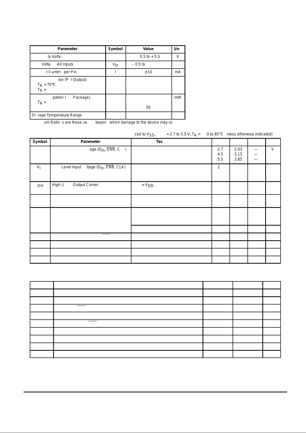
MAXIMUM RATINGS* (Voltages referenced to V
SS
)
Parameter
Symbol
Value
Unit
DC Supply Voltage
V
DD
– 0.5 to + 5.5
V
Input Voltage, All Inputs
V
in
– 0.5 to VDD + 0.5
V
DC Input Current, per Pin
I
± 10
mA
БББББББББ
Á
Power Dissipation (Per Output)
TA = 70°C
TA = 85°C
ÁÁ
Á
P
OH
БББББ
Á
50
20
Á
Á
mW
БББББББББ
Á
БББББББББ
Á
Power Dissipation (Per Package)
TA = 70°C
TA = 85°C
ÁÁ
Á
ÁÁ
Á
P
D
БББББ
Á
БББББ
Á
150
50
Á
Á
Á
Á
mW
Storage Temperature Range
T
stg
– 65 to + 150
°C
*Maximum Ratings are those values beyond which damage to the device may occur.
ELECTRICAL CHARACTERISTICS (Voltages referenced to V
SS
, VDD = 2.7 to 5.5 V , TA = – 40 to 85°C unless otherwise indicated)
Symbol
Parameter Test Conditions V
DD
Min Max Unit
V
IH
High–Level Input Voltage (Din, ENB, CLK) 2.7
4.5
5.5
2.03
3.15
3.85
—
—
—
V
V
IL
Low–Level Input Voltage (Din, ENB, CLK) 2.7
4.5
5.5
—
—
—
0.67
1.35
1.65
V
I
OH
High–Level Output Current (D
out
) V
out
= VDD – 0.5 V 2.7
4.5
0.3
1.1
—
—
mA
I
OL
Low–Level Output Current (D
out
) V
out
= 0.5 V 2.7
4.5
1.0
1.8
—
—
mA
I
SS
Quiescent Supply Current (per Package)
I
out
= 0 µA, All DAC Outputs = Zero 2.7
4.5
5.5
—
—
—
1.25
2.10
2.50
mA
I
out
= 0 µA, All DAC Outputs = Full Scale 5.5 — 30 µA
I
in
Input Leakage Current (Din, ENB, CLK) Vin = VDD or 0 V 5.5 — 1 µA
V
nonl
Integral Nonlinearity (Rn Out) See Figure 1 — – 1 1/4 1/4 LSB
V
step
Differential Nonlinearity (Rn Out) See Figure 2 — – 3/4 3/4 LSB
V
offset
Offset from V
SS
Din = $00, See Figure 1 —
1/4
1 3/4 LSB
SWITCHING CHARACTERISTICS
(VDD = 2.7 to 5.5 V , Voltages referenced to VSS, TA = – 40 to 85°C, CL = 50 pF, Input tr = tf = 20 ns unless otherwise indicated)
Symbol
Parameter Min Max Unit
t
wH
Positive Pulse Width, CLK (Figures 3 and 4) 166 — ns
t
wL
Negative Pulse Width, CLK (Figures 3 and 4) 166 — ns
t
su
Setup Time, ENB to CLK (Figures 3 and 4) 135 — ns
t
su
Setup Time, Din to CLK (Figures 3 and 4) 55 — ns
t
h
Hold Time, CLK to ENB (Figures 3 and 4) 135 — ns
t
h
Hold Time, CLK to Din (Figures 3 and 4) 55 — ns
tr, t
f
Input Rise and Fall Times, CLK — 100 µs
C
in
Input Capacitance — 10 pF
f
clk
Serial Data Clock Frequency (Refer to twH and twL Above) (Figures 3 and 4) dc 3 MHz
This device contains protection circuitry to
guard against damage due to high static
voltages or electric fields; however, it is advised that precautions be taken to avoid
application of voltage higher than maximum
rated voltages to this high–impedance circuit.
For proper operation it is recommended that
Vin and V
out
be constrained to the range VSS ≤
(Vin or V
out
) ≤VDD.
Unused inputs must always be tied to an
appropriate logic voltage level (e.g., either V
SS
or VDD).
 Loading...