

Motorola MC1436CD, MC1436CP1 Datasheet
Device
Operating
Temperature Range
Package
SEMICONDUCTOR
TECHNICAL DATA
OPERATIONAL AMPLIFIERS
ORDERING INFORMATION
MC1436CD,D
MC1436CP1,P1
TA = 0° to +70°C
SO–8
Plastic DIP
(Top View)
PIN CONNECTIONS
Order this document by MC1436/D
D SUFFIX
PLASTIC PACKAGE
CASE 751
(SO–8)
P1 SUFFIX
PLASTIC PACKAGE
CASE 626
1
1
8
8
N.C.
V
CC
Output
Offset Null
Offset Null
1
2
3
4
8
7
6
5
Noninv. Input
V
EE
Inv. Input
+
1
MOTOROLA ANALOG IC DEVICE DATA
The MC1436, C was designed for use as a summing amplifier, integrator,
or amplifier with operating characteristics as a function of the external
feedback components.
• Output Voltage Swing:
±22 V
pk(min)
(VCC = +28 V, VEE = –28 V)
• Fast Slew Rate: 2.0 V/µs Typ
• Internally Compensated
• Offset Voltage Null Capability
• Input Overvoltage Protection
• A
VOL
: 500,000 Typ
• Characteristics Independent of Power Supply Voltages:
(±5.0 Vdc to ±36 Vdc)
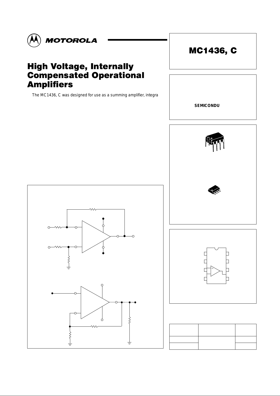
Figure 1. Differential Amplifier with ±20 V
Common Mode Input Voltage Range
Figure 2. Typical Noninverting X10 Voltage Amplifier
MC1436 , C
2
3
4
6
7
+28 V
VO = 10 (VB –VA)
R4
4.7 k
R2
100 k
R1
10 k
R3
470
V
A
V
B
+
–
–28 V
MC1436 , C
3
7 +28 V
6
4 –28 V
1.0 k
2
VO = 44 V
pp
VI = 4.4 V
pp
RL
≥
5.0 k
9.0 k
+
_
Motorola, Inc. 1996 Rev 5
MC1436, C
2
MOTOROLA ANALOG IC DEVICE DATA
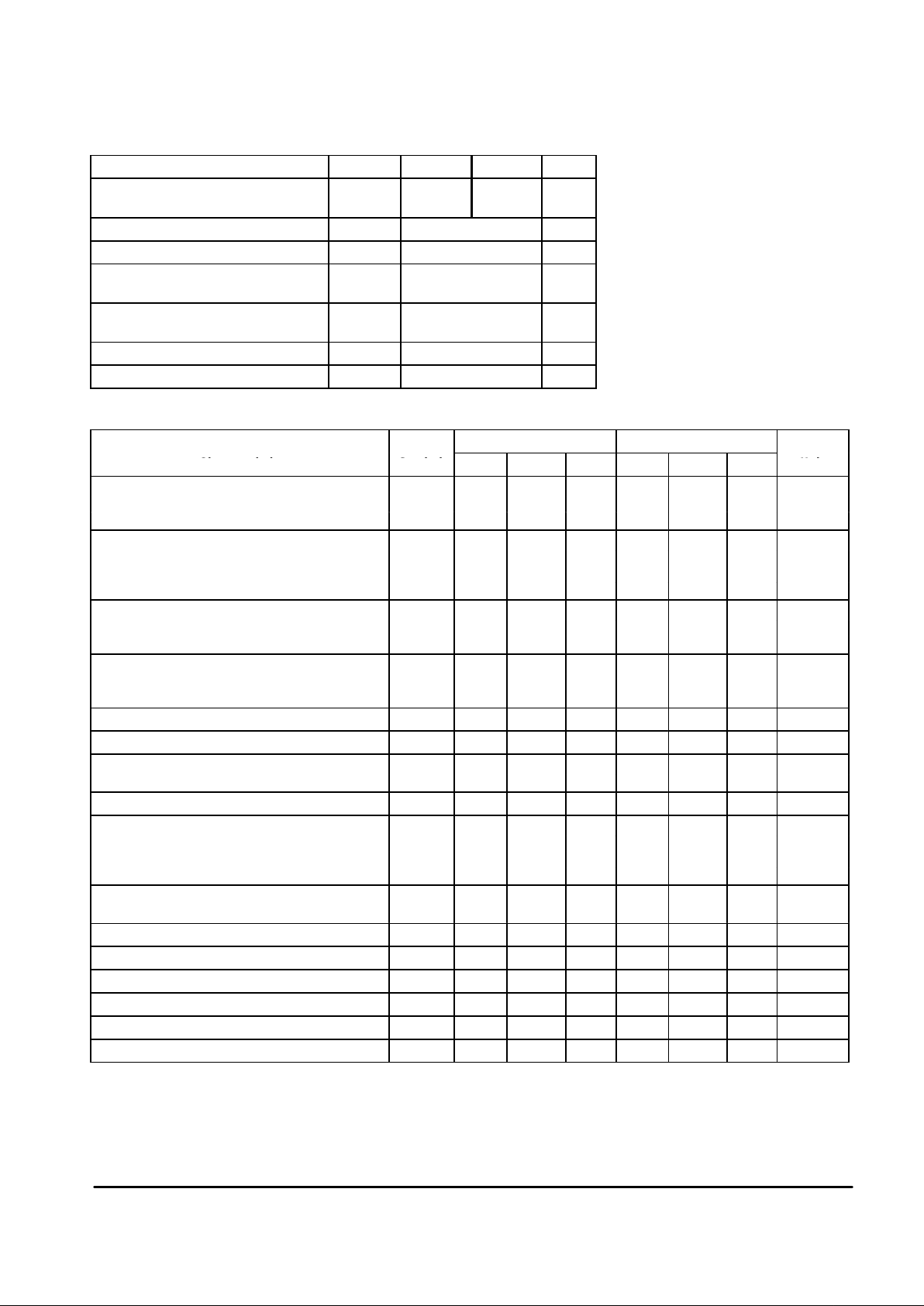
MAXIMUM RATINGS (T
A
= +25°C, unless otherwise noted.)
Rating Symbol MC1436 MC1436C Unit
Power Supply Voltage V
CC
V
EE
+34
–34
+30
–30
Vdc
Input Differential Voltage Range V
IDR
Note 2 V
Input Common Mode Voltage Range V
ICR
Note 2 V
Output Short Circuit Duration
(VCC = VEE = 28 Vdc, VO = 0)
t
SC
5.0 sec
Power Dissipation (Package Limitation)
Derate above TA = +25°C
P
D
680
4.6
mW
mW/°C
Operating Ambient Temperature Range T
A
0 to +70 °C
Storage Temperature Range T
stg
–65 to +150 °C
ELECTRICAL CHARACTERISTICS (V
CC
= +28 V , VEE = –28 V , TA = 25°C, unless otherwise noted.)
MC1436 MC1436C
Characteristic Symbol
Min Typ Max Min Typ Max
Unit
Input Bias Current I
IB
nAdc
TA = +25°C – 15 40 – 25 90
TA = T
low
to T
high
(See Note 1) – – 55 – – –
Input Offset Current I
IO
nAdc
TA = +25°C – 5.0 10 – 10 25
TA = +25°C to T
high
– – 14 – – –
TA = T
low
to +25°C – – 14 – – –
Input Offset Voltage V
IO
mVdc
TA = +25°C – 5.0 10 – 5.0 12
TA = T
low
to T
high
– – 14 – – –
Differential Input Impedance (Open loop, f ≤ 5.0 Hz) MΩ
Parallel Input Resistance rp – 10 – – 10 – pF
Parallel Input Capacitance Cp – 2.0 – – 2.0 –
Common Mode Input Impedance (f ≤ 5.0 Hz) z
ic
– 250 – – 250 – MΩ
Input Common Mode Voltage Range V
ICR
±22 ±25 – ±18 ±20 – Vpk
Equivalent Input Noise Voltage e
n
nV/(Hz)1/
2
(AV = 100, RS = 10 kΩ, f = 1.0 kHz, BW = 1.0 Hz) – 50 – – 50 –
Common Mode Rejection (DC) CMR 70 110 – 50 90 – dB
Large Signal DC Open Loop Voltage Gain A
VOL
V/V
(VO = ±10 V, RL = 100 kΩ)TA = +25°C 70,000 500,000 – 50,000 500,000 –
TA = T
low
to T
high
50,000 – – – – –
(VO = ±10 V, RL = 10 kΩ, TA = +25°C) – 200,000 – – 200,000 –
Power Bandwidth (Voltage Follower) BWp kHz
(AV = 1, RL = 5.0 kΩ, THD ≤ 5%, VO = 40 Vpp) – 23 – – 23 –
Unity Gain Crossover Frequency (Open loop) f
c
– 1.0 – – 1.0 – MHz
Phase Margin (Open loop, Unity Gain) φ
m
– 50 – – 50 – Degrees
Gain Margin A
M
– 18 – – 18 – dB
Slew Rate (Unity Gain) SR – 2.0 – – 2.0 – V/µs
Output Impedance (f ≤ 5.0 Hz) z
O
– 1.0 – – 1.0 – kΩ
Short Circuit Output Current I
SC
– ±17 – – ±19 – mAdc
NOTES: 1. T
low
= 0°C for MC1436,C T
high
= +70°C for MC1436,C
2.Either or both input voltages must not exceed the magnitude of VCC or VEE +3.0 V .
MC1436, C
3
MOTOROLA ANALOG IC DEVICE DATA
ELECTRICAL CHARACTERISTICS (V
CC
= +28 V , VEE = –28 V , TA = 25°C, unless otherwise noted.)
Characteristic Unit
MC1436CMC1436
Symbol
Characteristic UnitMaxTypMinMaxTypMinSymbol
Output Voltage Range (RL = 5.0 kΩ) V
O
V
pk
VCC = +28 Vdc, VEE = –28 Vdc ±20 ±22 – ±20 ±22 –
VCC = +36 Vdc, VEE = –36 Vdc – – – – – –
Power Supply Rejection µV/V
VEE = Constant, Rs ≤ 10 kΩ PSR + – 35 200 – 50 –
VCC = Constant, Rs ≤ 10 kΩ PSR – – 35 200 – 50 –
Power Supply Current (See Note 2) I
CC
I
EE
–
–
2.6
2.6
5.0
5.0
–
–
2.6
2.6
5.0
5.0
mAdc
DC Quiescent Power Consumption (VO = 0) P
C
– 146 280 – 146 280 mW
NOTES: 2. VCC = VEE = 5.0 Vdc to 30 Vdc for MC1436
VCC = VEE = 5.0 Vdc to 28 Vdc for MC1436C
Figure 3. Low–Drift Sample and Hold Figure 4. Power Bandwidth
Figure 5. Peak Output Voltage Swing versus
Power Supply Voltage
Figure 6. Open Loop Frequency Response
Switch
Sample
Command
1.0
µ
F
Polycarbonate
–28 V
1
10 k
5
6
*e
o
+28 V
2
3
e
i
*Drift due to bias current
is typically 8.0 mV s
7
4
MC1436
+
–
f, FREQUENCY (kHz)
70
60
50
40
30
20
10
0
4.0 6.0 8.0 10 20 40 60 80 100 200 400
2
3
7
+28 V
V
O
10 k
–28 V
6
4
V
O
, OUTPUT VOLTAGE (V )
p–p
VCC/VEE, POWER SUPPLY VOLTAGE (Vdc)
V , OUTPUT VOLTAGE SWING (V )
O
35
30
25
20
15
10
5.0
0
0 10 20 30 40
RL = 5.0 k
Ω
TA = 25° C
f, FREQUENCY (kHz)
A , VOLTAGE GAIN (dB)
VOL
140
120
100
80
60
40
20
0
–20
1.0 10 100 1.0 k 10 k 100 k 1.0 M 10 M 100 M
pk
 Loading...