

MOTOROLA MC14082BDR2, MC14082BF, MC14082BFR2, MC14082BCP, MC14081BFL2 Datasheet
...
Semiconductor Components Industries, LLC, 2000
March, 2000 – Rev. 1
1 Publication Order Number:
MC14001B/D
MC14001B Series
B-Suffix Series CMOS Gates
MC14001B, MC14011B, MC14023B,
MC14025B, MC14071B, MC14073B,
MC14081B, MC14082B
The B Series logic gates are constructed with P and N channel
enhancement mode devices in a single monolithic structure
(Complementary MOS). Their primary use is where low power
dissipation and/or high noise immunity is desired.
• Supply Voltage Range = 3.0 Vdc to 18 Vdc
• All Outputs Buffered
• Capable of Driving Two Low–power TTL Loads or One Low–power
Schottky TTL Load Over the Rated Temperature Range.
• Double Diode Protection on All Inputs Except: Triple Diode
Protection on MC14011B and MC14081B
• Pin–for–Pin Replacements for Corresponding CD4000 Series B
Suffix Devices
MAXIMUM RATINGS (Voltages Referenced to V
SS
) (Note 1.)
Symbol Parameter Value Unit
V
DD
DC Supply Voltage Range –0.5 to +18.0 V
Vin, V
out
Input or Output Voltage Range
(DC or Transient)
–0.5 to VDD + 0.5 V
Iin, I
out
Input or Output Current
(DC or Transient) per Pin
±10 mA
P
D
Power Dissipation,
per Package (Note 2.)
500 mW
T
A
Ambient Temperature Range –55 to +125 °C
T
stg
Storage Temperature Range –65 to +150 °C
T
L
Lead Temperature
(8–Second Soldering)
260 °C
1. Maximum Ratings are those values beyond which damage to the device
may occur.
2. Temperature Derating:
Plastic “P and D/DW” Packages: – 7.0 mW/_C From 65_C T o 125_C
This device contains protection circuitry to guard against damage due to high
static voltages or electric fields. However, precautions must be taken to avoid
applications of any voltage higher than maximum rated voltages to this
high–impedance circuit. For proper operation, V
in
and V
out
should be constrained
to the range V
SS
v (Vin or V
out
) v VDD.
Unused inputs must always be tied to an appropriate logic voltage level (e.g.,
either V
SS
or VDD). Unused outputs must be left open.
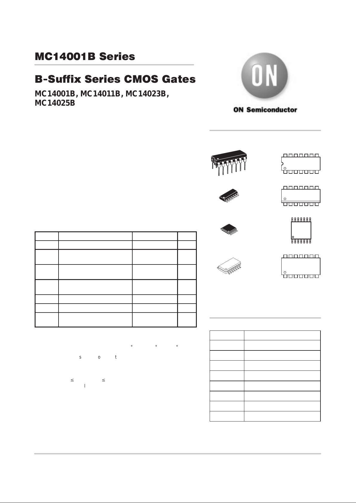
http://onsemi.com
Device Description
DEVICE INFORMATION
MC14001B Quad 2–Input NOR Gate
MC1401 1B Quad 2–Input NAND Gate
MC14023B Triple 3–Input NAND Gate
MC14025B Triple 3–Input NOR Gate
MC14071B Quad 2–Input OR Gate
MARKING
DIAGRAMS
1
14
PDIP–14
P SUFFIX
CASE 646
MC140XXBCP
AWLYYWW
SOIC–14
D SUFFIX
CASE 751A
TSSOP–14
DT SUFFIX
CASE 948G
1
14
140XXB
AWLYWW
14
0XXB
ALYW
1
14
XX = Specific Device Code
A = Assembly Location
WL or L = Wafer Lot
YY or Y = Year
WW or W = Work Week
SOEIAJ–14
F SUFFIX
CASE 965
1
14
MC140XXB
AWLYWW
MC14073B Triple 3–Input AND Gate
MC14081B Quad 2–Input AND Gate
MC14082B Dual 4–Input AND Gate
See detailed ordering and shipping information in the package
dimensions section on page 1 1 of this data sheet.
ORDERING INFORMATION
MC14001B Series
http://onsemi.com
2
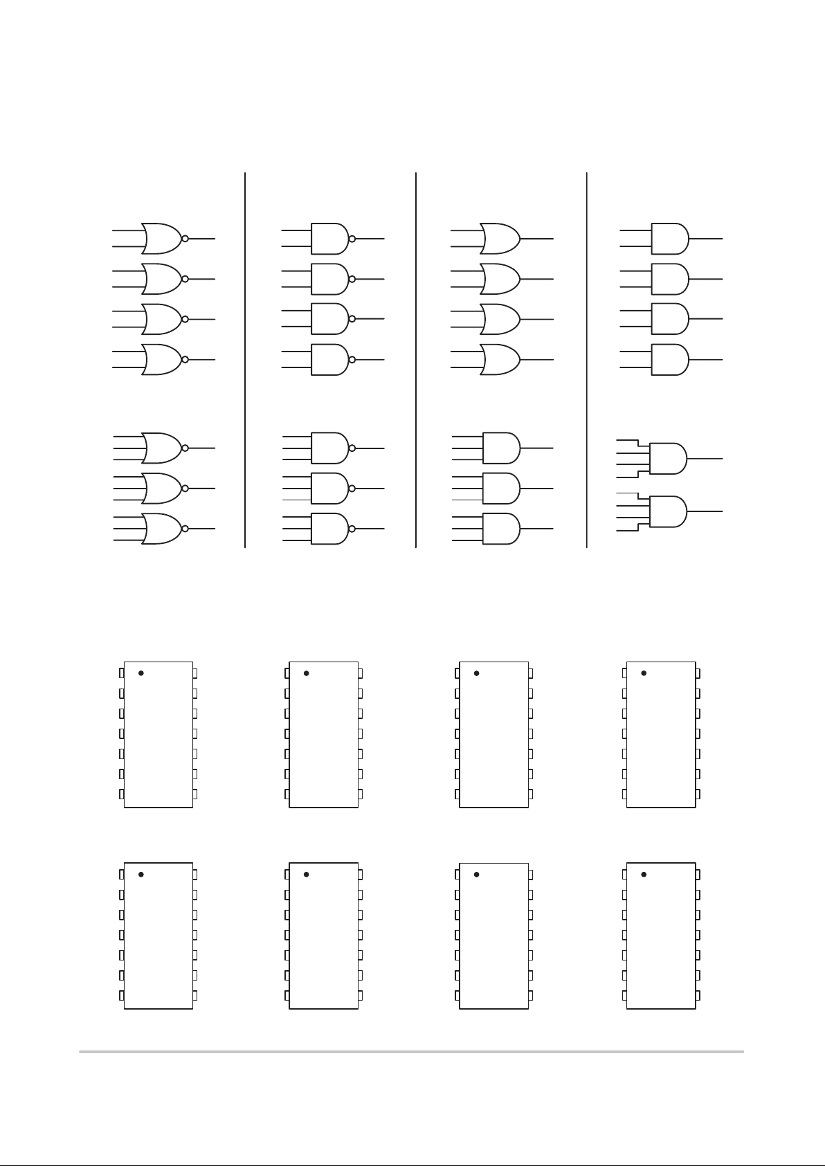
LOGIC DIAGRAMS
1
2
5
6
8
9
12
13
3
4
10
11
1
2
5
6
8
9
12
13
3
4
10
11
1
2
5
6
8
9
12
13
3
4
10
11
1
2
5
6
8
9
12
13
3
4
10
11
2 INPUT
1
2
9
3 INPUT
8
3
4
6
5
11
12
10
13
1
2
9
8
3
4
6
5
11
12
10
13
1
2
9
8
3
4
6
5
11
12
10
13
1
13
3
4
5
2
10
11
12
9
NC = 6, 8
VDD = PIN 14
V
SS
= PIN 7
FOR ALL DEVICES
NOR
MC14001B
Quad 2–Input NOR Gate
MC14025B
Triple 3–Input NOR Gate
MC14023B
Triple 3–Input NAND Gate
NAND
MC14011B
Quad 2–Input NAND Gate
OR
MC14071B
Quad 2–Input OR Gate
AND
MC14081B
Quad 2–Input AND Gate
MC14073B
Triple 3–Input AND Gate
MC14082B
Dual 4–Input AND Gate
PIN ASSIGNMENTS
11
12
13
14
8
9
105
4
3
2
1
7
6
OUT
C
OUT
D
IN 1
D
IN 2
D
V
DD
IN 1
C
IN 2
C
OUT
B
OUT
A
IN 2
A
IN 1
A
V
SS
IN 2
B
IN 1
B
11
12
13
14
8
9
105
4
3
2
1
7
6
OUT
C
OUT
D
IN 1
D
IN 2
D
V
DD
IN 1
C
IN 2
C
OUT
B
OUT
A
IN 2
A
IN 1
A
V
SS
IN 2
B
IN 1
B
11
12
13
14
8
9
105
4
3
2
1
7
6
OUT
C
IN 1
C
IN 2
C
IN 3
C
V
DD
IN 3
A
OUT
A
IN 2
B
IN 1
B
IN 2
A
IN 1
A
V
SS
OUT
B
IN 3
B
11
12
13
14
8
9
105
4
3
2
1
7
6
OUT
C
IN 1
C
IN 2
C
IN 3
C
V
DD
IN 3
A
OUT
A
IN 2
B
IN 1
B
IN 2
A
IN 1
A
V
SS
OUT
B
IN 3
B
11
12
13
14
8
9
105
4
3
2
1
7
6
OUT
C
OUT
D
IN 1
D
IN 2
D
V
DD
IN 1
C
IN 2
C
OUT
B
OUT
A
IN 2
A
IN 1
A
V
SS
IN 2
B
IN 1
B
11
12
13
14
8
9
105
4
3
2
1
7
6
OUT
C
IN 1
C
IN 2
C
IN 3
C
V
DD
IN 3
A
OUT
A
IN 2
B
IN 1
B
IN 2
A
IN 1
A
V
SS
OUT
B
IN 3
B
11
12
13
14
8
9
105
4
3
2
1
7
6
OUT
C
OUT
D
IN 1
D
IN 2
D
V
DD
IN 1
C
IN 2
C
OUT
B
OUT
A
IN 2
A
IN 1
A
V
SS
IN 2
B
IN 1
B
11
12
13
14
8
9
105
4
3
2
1
7
6
IN 2
B
IN 3
B
IN 4
B
OUT
B
V
DD
NC
IN 1
B
IN 3
A
IN 2
A
IN 1
A
OUT
A
V
SS
NC
IN 4
A
NC = NO CONNECTION
MC14023B
Triple 3–Input NAND Gate
MC14001B
Quad 2–Input NOR Gate
MC14011B
Quad 2–Input NAND Gate
MC14082B
Dual 4–Input AND Gate
MC14081B
Quad 2–Input AND Gate
MC14025B
Triple 3–Input NOR Gate
MC14071B
Quad 2–Input OR Gate
MC14073B
Triple 3–Input AND Gate
MC14001B Series
http://onsemi.com
3
ELECTRICAL CHARACTERISTICS (Voltages Referenced to V
SS
)
V
– 55_C
25_C
125_C
Characteristic
Symbol
V
DD
Vdc
Min
Max
Min
Typ
(3.)
Max
Min
Max
Unit
ОООООООО
Î
Output Voltage “0” Level
V
in
= VDD or 0
ÎÎ
Î
V
OL
Î
Î
5.0
10
15
Î
Î
—
—
—
Î
Î
0.05
0.05
0.05
ÎÎ
Î
—
—
—
Î
Î
0
0
0
ÎÎ
Î
0.05
0.05
0.05
Î
Î
—
—
—
Î
Î
0.05
0.05
0.05
Î
Î
Vdc
ОООООООО
Î
“1” Level
V
in
= 0 or V
DD
ÎÎ
Î
V
OH
Î
Î
5.0
10
15
Î
Î
4.95
9.95
14.95
Î
Î
—
—
—
ÎÎ
Î
4.95
9.95
14.95
Î
Î
5.0
10
15
ÎÎ
Î
—
—
—
Î
Î
4.95
9.95
14.95
Î
Î
—
—
—
Î
Î
Vdc
ОООООООО
Î
ОООООООО
Î
Input Voltage “0” Level
(V
O
= 4.5 or 0.5 Vdc)
(V
O
= 9.0 or 1.0 Vdc)
(V
O
= 13.5 or 1.5 Vdc)
ÎÎ
Î
ÎÎ
Î
V
IL
Î
Î
Î
Î
5.0
10
15
Î
Î
Î
Î
—
—
—
Î
Î
Î
Î
1.5
3.0
4.0
ÎÎ
Î
ÎÎ
Î
—
—
—
Î
Î
Î
Î
2.25
4.50
6.75
ÎÎ
Î
ÎÎ
Î
1.5
3.0
4.0
Î
Î
Î
Î
—
—
—
Î
Î
Î
Î
1.5
3.0
4.0
Î
Î
Î
Î
Vdc
ОООООООО
Î
ОООООООО
Î
“1” Level
(V
O
= 0.5 or 4.5 Vdc)
(V
O
= 1.0 or 9.0 Vdc)
(V
O
= 1.5 or 13.5 Vdc)
ÎÎ
Î
ÎÎ
Î
V
IH
Î
Î
Î
Î
5.0
10
15
Î
Î
Î
Î
3.5
7.0
11
Î
Î
Î
Î
—
—
—
ÎÎ
Î
ÎÎ
Î
3.5
7.0
11
Î
Î
Î
Î
2.75
5.50
8.25
ÎÎ
Î
ÎÎ
Î
—
—
—
Î
Î
Î
Î
3.5
7.0
11
Î
Î
Î
Î
—
—
—
Î
Î
Î
Î
Vdc
ОООООООО
Î
ОООООООО
Î
ОООООООО
Î
Output Drive Current
(V
OH
= 2.5 Vdc) Source
(V
OH
= 4.6 Vdc)
(V
OH
= 9.5 Vdc)
(V
OH
= 13.5 Vdc)
ÎÎ
Î
ÎÎ
Î
ÎÎ
Î
I
OH
Î
Î
Î
Î
Î
Î
5.0
5.0
10
15
Î
Î
Î
Î
Î
Î
– 3.0
– 0.64
– 1.6
– 4.2
Î
Î
Î
Î
Î
Î
—
—
—
—
ÎÎ
Î
ÎÎ
Î
ÎÎ
Î
– 2.4
– 0.51
– 1.3
– 3.4
Î
Î
Î
Î
Î
Î
– 4.2
– 0.88
– 2.25
– 8.8
ÎÎ
Î
ÎÎ
Î
ÎÎ
Î
—
—
—
—
Î
Î
Î
Î
Î
Î
– 1.7
– 0.36
– 0.9
– 2.4
Î
Î
Î
Î
Î
Î
—
—
—
—
Î
Î
Î
Î
Î
Î
mAdc
ОООООООО
Î
(VOL = 0.4 Vdc) Sink
(V
OL
= 0.5 Vdc)
(V
OL
= 1.5 Vdc)
ÎÎ
Î
I
OL
Î
Î
5.0
10
15
Î
Î
0.64
1.6
4.2
Î
Î
—
—
—
ÎÎ
Î
0.51
1.3
3.4
Î
Î
0.88
2.25
8.8
ÎÎ
Î
—
—
—
Î
Î
0.36
0.9
2.4
Î
Î
—
—
—
Î
Î
mAdc
Input Current
I
in
15
—
± 0.1
—
±0.00001
± 0.1
—
± 1.0
µAdc
ОООООООО
Î
Input Capacitance
(V
in
= 0)
ÎÎ
Î
C
in
Î
Î
—
Î
Î
—
Î
Î
—
ÎÎ
Î
—
Î
Î
5.0
ÎÎ
Î
7.5
Î
Î
—
Î
Î
—
Î
Î
pF
ОООООООО
Î
Quiescent Current
(Per Package)
ÎÎ
Î
I
DD
Î
Î
5.0
10
15
Î
Î
—
—
—
Î
Î
0.25
0.5
1.0
ÎÎ
Î
—
—
—
Î
Î
0.0005
0.0010
0.0015
ÎÎ
Î
0.25
0.5
1.0
Î
Î
—
—
—
Î
Î
7.5
15
30
Î
Î
µAdc
ОООООООО
Î
ОООООООО
Î
Total Supply Current
(4.) (5.)
(Dynamic plus Quiescent,
Per Gate, C
L
= 50 pF)
ÎÎ
Î
ÎÎ
Î
I
T
Î
Î
Î
Î
5.0
10
15
ООООООООООООООО
Î
ООООООООООООООО
Î
IT = (0.3 µA/kHz) f + IDD/N
I
T
= (0.6 µA/kHz) f + IDD/N
I
T
= (0.9 µA/kHz) f + IDD/N
Î
Î
Î
Î
µAdc
3. Data labelled “Typ” is not to be used for design purposes but is intended as an indication of the IC’s potential performance.
4. The formulas given are for the typical characteristics only at 25_C.
5. To calculate total supply current at loads other than 50 pF:
I
T(CL
) = IT(50 pF) + (CL – 50) Vfk
where: I
T
is in µA (per package), CL in pF, V = (VDD – VSS) in volts, f in kHz is input frequency, and k = 0.001 x the number of exercised gates
per package.
MC14001B Series
http://onsemi.com
4
B–SERIES GATE SWITCHING TIMES
SWITCHING CHARACTERISTICS
(6.)
(CL = 50 pF, T
A
= 25_C)
ООООООООООООО
Î
Characteristic
ÎÎÎ
Î
Symbol
ÎÎ
Î
V
DD
Vdc
ÎÎ
Î
Min
ÎÎ
Î
Typ
(7.)
ÎÎ
Î
Max
Î
Î
Unit
ООООООООООООО
Î
ООООООООООООО
Î
Output Rise Time, All B–Series Gates
t
TLH
= (1.35 ns/pF) CL + 33 ns
t
TLH
= (0.60 ns/pF) CL + 20 ns
t
TLH
= (0.40 ns/PF) CL + 20 ns
ÎÎÎ
Î
ÎÎÎ
Î
t
TLH
ÎÎ
Î
ÎÎ
Î
5.0
10
15
ÎÎ
Î
ÎÎ
Î
—
—
—
ÎÎ
Î
ÎÎ
Î
100
50
40
ÎÎ
Î
ÎÎ
Î
200
100
80
Î
Î
Î
Î
ns
ООООООООООООО
Î
ООООООООООООО
Î
Output Fall Time, All B–Series Gates
t
THL
= (1.35 ns/pF) CL + 33 ns
t
THL
= (0.60 ns/pF) CL + 20 ns
t
THL
= (0.40 ns/pF) CL + 20 ns
ÎÎÎ
Î
ÎÎÎ
Î
t
THL
ÎÎ
Î
ÎÎ
Î
5.0
10
15
ÎÎ
Î
ÎÎ
Î
—
—
—
ÎÎ
Î
ÎÎ
Î
100
50
40
ÎÎ
Î
ÎÎ
Î
200
100
80
Î
Î
Î
Î
ns
ООООООООООООО
Î
ООООООООООООО
Î
ООООООООООООО
Î
ООООООООООООО
Î
ООООООООООООО
Î
ООООООООООООО
Î
ООООООООООООО
Î
ООООООООООООО
Î
Propagation Delay Time
MC14001B, MC14011B only
t
PLH
, t
PHL
= (0.90 ns/pF) CL + 80 ns
t
PLH
, t
PHL
= (0.36 ns/pF) CL + 32 ns
t
PLH
, t
PHL
= (0.26 ns/pF) CL + 27 ns
All Other 2, 3, and 4 Input Gates
t
PLH
, t
PHL
= (0.90 ns/pF) CL + 115 ns
t
PLH
, t
PHL
= (0.36 ns/pF) CL + 47 ns
t
PLH
, t
PHL
= (0.26 ns/pF) CL + 37 ns
8–Input Gates (MC14068B, MC14078B)
t
PLH
, t
PHL
= (0.90 ns/pF) CL + 155 ns
t
PLH
, t
PHL
= (0.36 ns/pF) CL + 62 ns
t
PLH
, t
PHL
= (0.26 ns/pF) CL + 47 ns
ÎÎÎ
Î
ÎÎÎ
Î
ÎÎÎ
Î
ÎÎÎ
Î
ÎÎÎ
Î
ÎÎÎ
Î
ÎÎÎ
Î
ÎÎÎ
Î
t
PLH
, t
PHL
ÎÎ
Î
ÎÎ
Î
ÎÎ
Î
ÎÎ
Î
ÎÎ
Î
ÎÎ
Î
ÎÎ
Î
ÎÎ
Î
5.0
10
15
5.0
10
15
5.0
10
15
ÎÎ
Î
ÎÎ
Î
ÎÎ
Î
ÎÎ
Î
ÎÎ
Î
ÎÎ
Î
ÎÎ
Î
ÎÎ
Î
—
—
—
—
—
—
—
—
—
ÎÎ
Î
ÎÎ
Î
ÎÎ
Î
ÎÎ
Î
ÎÎ
Î
ÎÎ
Î
ÎÎ
Î
ÎÎ
Î
125
50
40
160
65
50
200
80
60
ÎÎ
Î
ÎÎ
Î
ÎÎ
Î
ÎÎ
Î
ÎÎ
Î
ÎÎ
Î
ÎÎ
Î
ÎÎ
Î
250
100
80
300
130
100
350
150
110
Î
Î
Î
Î
Î
Î
Î
Î
Î
Î
Î
Î
Î
Î
Î
Î
ns
6. The formulas given are for the typical characteristics only at 25_C.
7. Data labelled “Typ” is not to be used for design purposes but is intended as an indication of the IC’s potential performance.
V
DD
14
C
L
VSS7
PULSE
GENERATOR
INPUT
OUTPUT
90%
50%
10%
10%
50%
90%
20 ns 20 ns
t
PHL
t
PLH
t
TLH
t
THL
V
OL
V
OH
0 V
V
DD
INPUT
OUTPUT
INVERTING
*All unused inputs of AND, NAND gates must be connected to VDD.
All unused inputs of OR, NOR gates must be connected to V
SS
.
90%
50%
10%
V
OL
V
OH
OUTPUT
NON–INVERTING
t
THL
t
TLH
t
PLH
t
PHL
*
Figure 1. Switching Time Test Circuit and Waveforms
 Loading...