

Motorola MC14060BD, MC14060BCL, MC14060BCP Datasheet
MOTOROLA CMOS LOGIC DATA
1
MC14060B
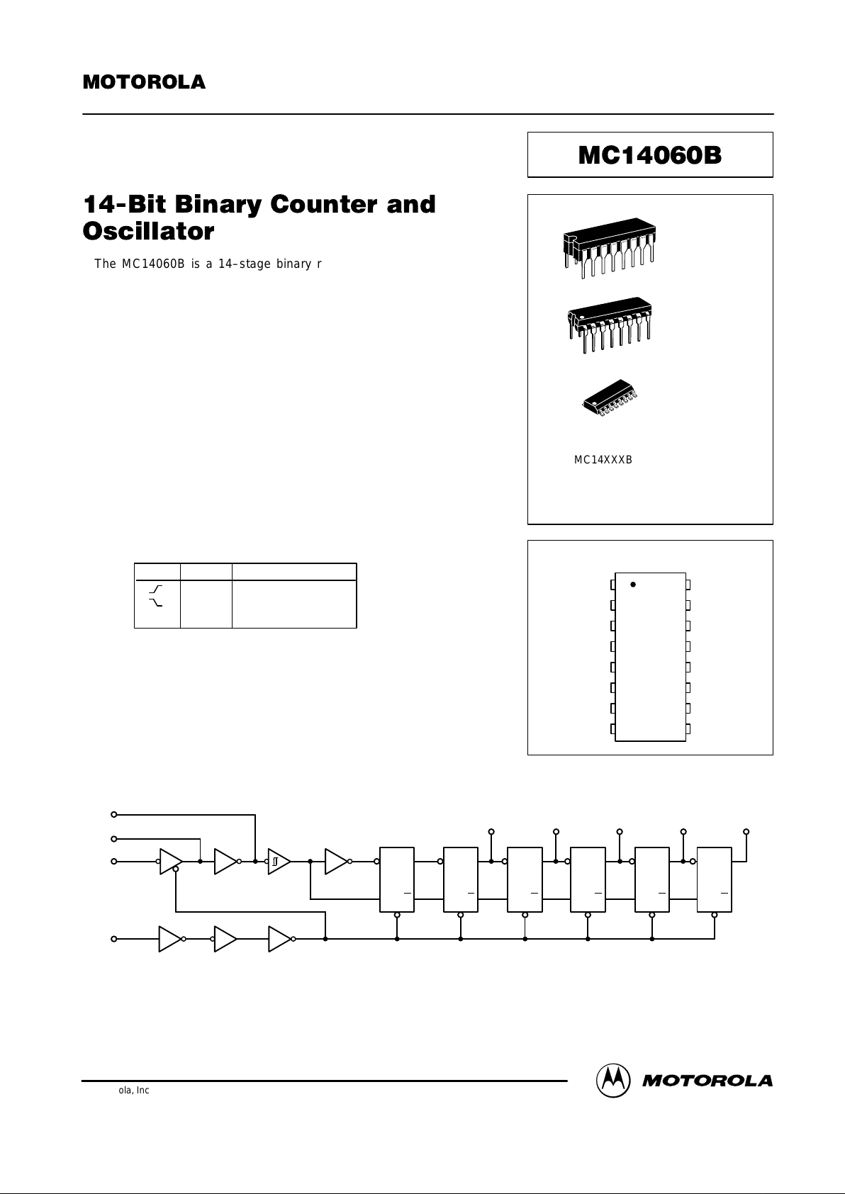
The MC14060B is a 14–stage binary ripple counter with an on–chip
oscillator buffer. The oscillator configuration allows design of either RC or
crystal oscillator circuits. Also included on the chip is a reset function which
places all outputs into the zero state and disables the oscillator. A negative
transition on Clock will advance the counter to the next state. Schmitt trigger
action on t he input l ine p ermits v ery slow input r ise a nd fall times.
Applications include time delay circuits, counter controls, and frequency
dividing circuits.
• Fully static operation
• Diode Protection on All Inputs
• Supply Voltage Range = 3.0 V to 18 V
• Capable of Driving Two Low–power TTL Loads or One Low–power
Schottky TTL Load Over the Rated Temperature Range
• Buffered Outputs Available from Stages 4 Through 10 and
12 Through 14
• Common Reset Line
• Pin–for–Pin Replacement for CD4060B
TRUTH TABLE
Clock Reset Output State
L No Change
L Advance to next state
X H All Outputs are low
X = Don’t Care
LOGIC DIAGRAM
OUT 2
OUT 1
CLOCK
RESET
12
11
10
9
Q4 Q5 Q12 Q13 Q14
57 1 2 3
C Q
R
C Q
C Q
R
C Q
C Q
R
C Q
C Q
R
C Q
C Q
R
C Q
C Q
R
C Q
Q6 = PIN 4
Q7 = PIN 6
Q8 = PIN 14
Q9 = PIN 13
Q10 = PIN 15 VDD = PIN 16
VSS = PIN 8
SEMICONDUCTOR TECHNICAL DATA
Motorola, Inc. 1995
REV 3
1/94
L SUFFIX
CERAMIC
CASE 620
ORDERING INFORMATION
MC14XXXBCP Plastic
MC14XXXBCL Ceramic
MC14XXXBD SOIC
TA = – 55° to 125°C for all packages.
P SUFFIX
PLASTIC
CASE 648
D SUFFIX
SOIC
CASE 751B
PIN ASSIGNMENT
13
14
15
16
9
10
11
125
4
3
2
1
8
7
6
RESET
Q9
Q8
Q10
V
DD
OUT 2
OUT 1
CLOCK
Q6
Q13
Q12
V
SS
Q4
Q7
Q5
Q14
MOTOROLA CMOS LOGIC DATAMC14060B
2
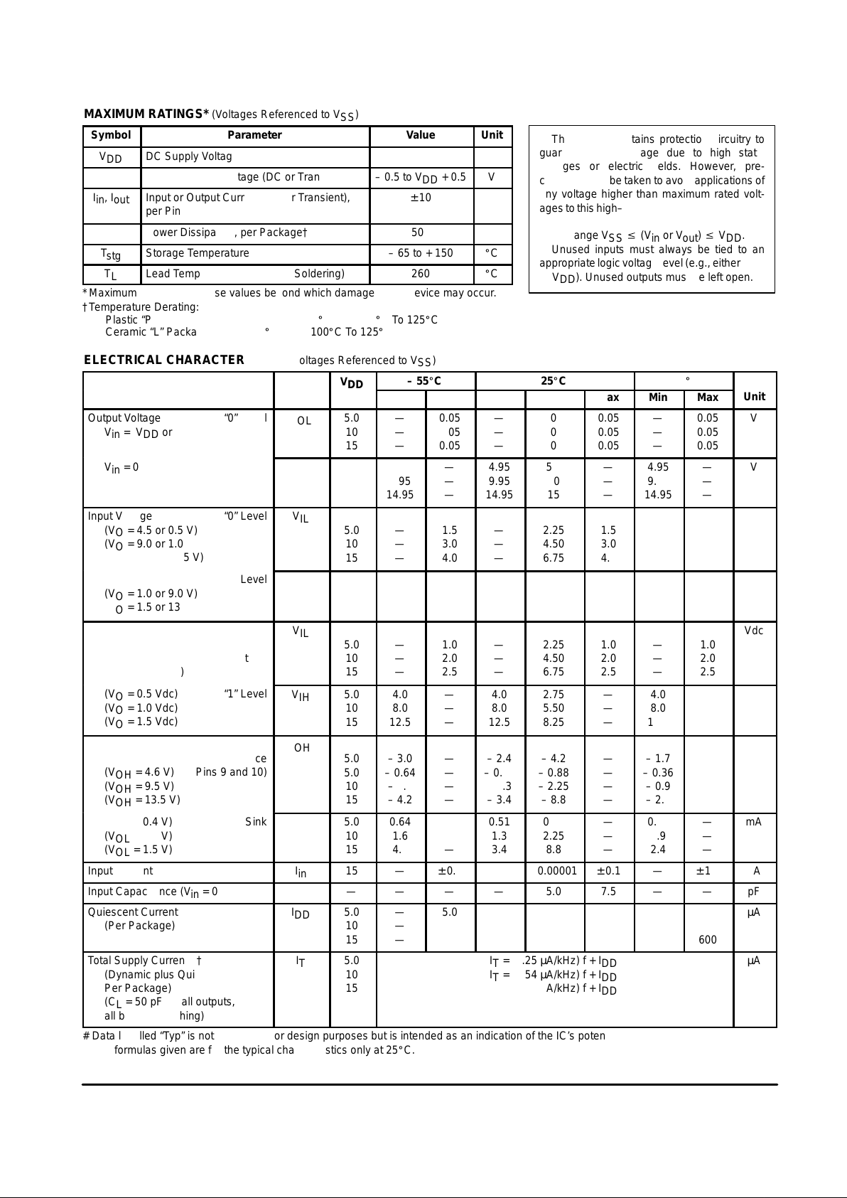
MAXIMUM RATINGS* (Voltages Referenced to V
SS
)
Symbol
Parameter
Value
Unit
V
DD
DC Supply Voltage
– 0.5 to + 18.0
V
Vin, V
out
Input or Output Voltage (DC or Transient)
– 0.5 to VDD + 0.5
V
Iin, I
out
Input or Output Current (DC or Transient),
per Pin
± 10
mA
P
D
Power Dissipation, per Package†
500
mW
T
stg
Storage Temperature
– 65 to + 150
_
C
T
L
Lead Temperature (8–Second Soldering)
260
_
C
*Maximum Ratings are those values beyond which damage to the device may occur.
†Temperature Derating:
Plastic “P and D/DW” Packages: – 7.0 mW/_C From 65_C To 125_C
Ceramic “L” Packages – 12 mW/_C From 100_C To 125_C
ELECTRICAL CHARACTERISTICS (Voltages Referenced to V
SS
)
V
DD
– 55_C
25_C
125_C
Characteristic
Symbol
V
DD
Vdc
Min
ÎÎÎ
ÎÎÎ
ÎÎÎ
Max
Min
Typ #
Max
Min
Max
Unit
Output Voltage “0” Level
Vin = VDD or 0
V
OL
5.0
10
15
—
—
—
ÎÎÎ
ÎÎÎ
ÎÎÎ
ÎÎÎ
ÎÎÎ
0.05
0.05
0.05
—
—
—
0
0
0
0.05
0.05
0.05
—
—
—
0.05
0.05
0.05
V
Vin = 0 or V
DD
“1” Level
V
OH
5.0
10
15
4.95
9.95
14.95
ÎÎÎ
ÎÎÎ
ÎÎÎ
ÎÎÎ
—
—
—
4.95
9.95
14.95
5.0
10
15
—
—
—
4.95
9.95
14.95
—
—
—
V
Input Voltage
“0” Level
(VO = 4.5 or 0.5 V)
(VO = 9.0 or 1.0 V)
(VO = 13.5 or 1.5 V)
V
IL
5.0
10
15
—
—
—
ÎÎÎ
ÎÎÎ
ÎÎÎ
ÎÎÎ
ÎÎÎ
1.5
3.0
4.0
—
—
—
2.25
4.50
6.75
1.5
3.0
4.0
—
—
—
1.5
3.0
4.0
V
(VO = 0.5 or 4.5 V)
“1” Level
(VO = 1.0 or 9.0 V)
(VO = 1.5 or 13.5 V)
V
IH
5.0
10
15
3.5
7.0
11.0
ÎÎÎ
ÎÎÎ
ÎÎÎ
ÎÎÎ
—
—
—
3.5
7.0
11.0
2.75
5.50
8.25
—
—
—
3.5
7.0
11.0
—
—
—
V
Input Voltage
“0” Level
(VO = 4.5 Vdc) (For Input 11
(VO = 9.0 Vdc) and Output 10)
(VO = 13.5 Vdc)
V
IL
5.0
10
15
—
—
—
ÎÎÎ
ÎÎÎ
ÎÎÎ
ÎÎÎ
ÎÎÎ
1.0
2.0
2.5
—
—
—
2.25
4.50
6.75
1.0
2.0
2.5
—
—
—
1.0
2.0
2.5
Vdc
(VO = 0.5 Vdc)
“1” Level
(VO = 1.0 Vdc)
(VO = 1.5 Vdc)
V
IH
5.0
10
15
4.0
8.0
12.5
ÎÎÎ
ÎÎÎ
ÎÎÎ
ÎÎÎ
ÎÎÎ
—
—
—
4.0
8.0
12.5
2.75
5.50
8.25
—
—
—
4.0
8.0
12.5
—
—
—
Vdc
Output Drive Current
(VOH = 2.5 V) (Except Source
(VOH = 4.6 V)
Pins 9 and 10)
(VOH = 9.5 V)
(VOH = 13.5 V)
I
OH
5.0
5.0
10
15
– 3.0
– 0.64
– 1.6
– 4.2
ÎÎÎ
ÎÎÎ
ÎÎÎ
ÎÎÎ
ÎÎÎ
—
—
—
—
– 2.4
– 0.51
– 1.3
– 3.4
– 4.2
– 0.88
– 2.25
– 8.8
—
—
—
—
– 1.7
– 0.36
– 0.9
– 2.4
—
—
—
—
mA
(VOL = 0.4 V) Sink
(VOL = 0.5 V)
(VOL = 1.5 V)
I
OL
5.0
10
15
0.64
1.6
4.2
ÎÎÎ
ÎÎÎ
ÎÎÎ
ÎÎÎ
ÎÎÎ
—
—
—
0.51
1.3
3.4
0.88
2.25
8.8
—
—
—
0.36
0.9
2.4
—
—
—
mA
Input Current
I
in
15
—
ÎÎÎ
ÎÎÎ
ÎÎÎ
± 0.1
—
±0.00001
± 0.1
—
± 1.0
µA
Input Capacitance (Vin = 0)
C
in
—
—
ÎÎÎ
ÎÎÎ
ÎÎÎ
—
—
5.0
7.5
—
—
pF
Quiescent Current
(Per Package)
I
DD
5.0
10
15
—
—
—
ÎÎÎ
ÎÎÎ
ÎÎÎ
ÎÎÎ
5.0
10
20
—
—
—
0.005
0.010
0.015
5.0
10
20
—
—
—
150
300
600
µA
Total Supply Current**†
(Dynamic plus Quiescent,
Per Package)
(CL = 50 pF on all outputs,
all buffers switching)
I
T
5.0
10
15
IT = (0.25 µA/kHz) f + I
DD
IT = (0.54 µA/kHz) f + I
DD
IT = (0.85 µA/kHz) f + I
DD
µA
# Data labelled “Typ” is not to be used for design purposes but is intended as an indication of the IC’s potential performance.
**The formulas given are for the typical characteristics only at 25_C.
This device contains protection circuitry to
guard against damage due to high static
voltages or electric fields. However, precautions must be taken to avoid applications of
any voltage higher than maximum rated voltages to this high–impedance circuit. For proper
operation, Vin and V
out
should be constrained
to the range VSS v (Vin or V
out
) v VDD.
Unused inputs must always be tied to an
appropriate logic voltage level (e.g., either V
SS
or VDD). Unused outputs must be left open.
 Loading...