

Motorola MC14050BD, MC14050BCL, MC14050BCP, MC14049BD, MC14049BCL Datasheet
...
MOTOROLA CMOS LOGIC DATA
1
MC14049B MC14050B
The MC14049B Hex Inverter/Buffer and MC14050B Noninverting Hex
Buffer are constructed with MOS P–Channel and N–Channel enhancement
mode devices in a single monolithic structure. These complementary MOS
devices find primary use where low power dissipation and/or high noise
immunity is desired. These devices provide logic level conversion using only
one supply voltage, VDD.
The input–signal high level (VIH) can exceed the VDD supply voltage for
logic level conversions. Two TTL/DTL loads can be driven when the devices
are used as a CMOS–to–TTL/DTL converter (VDD = 5.0 V, VOL v 0.4 V,
IOL ≥ 3.2 mA).
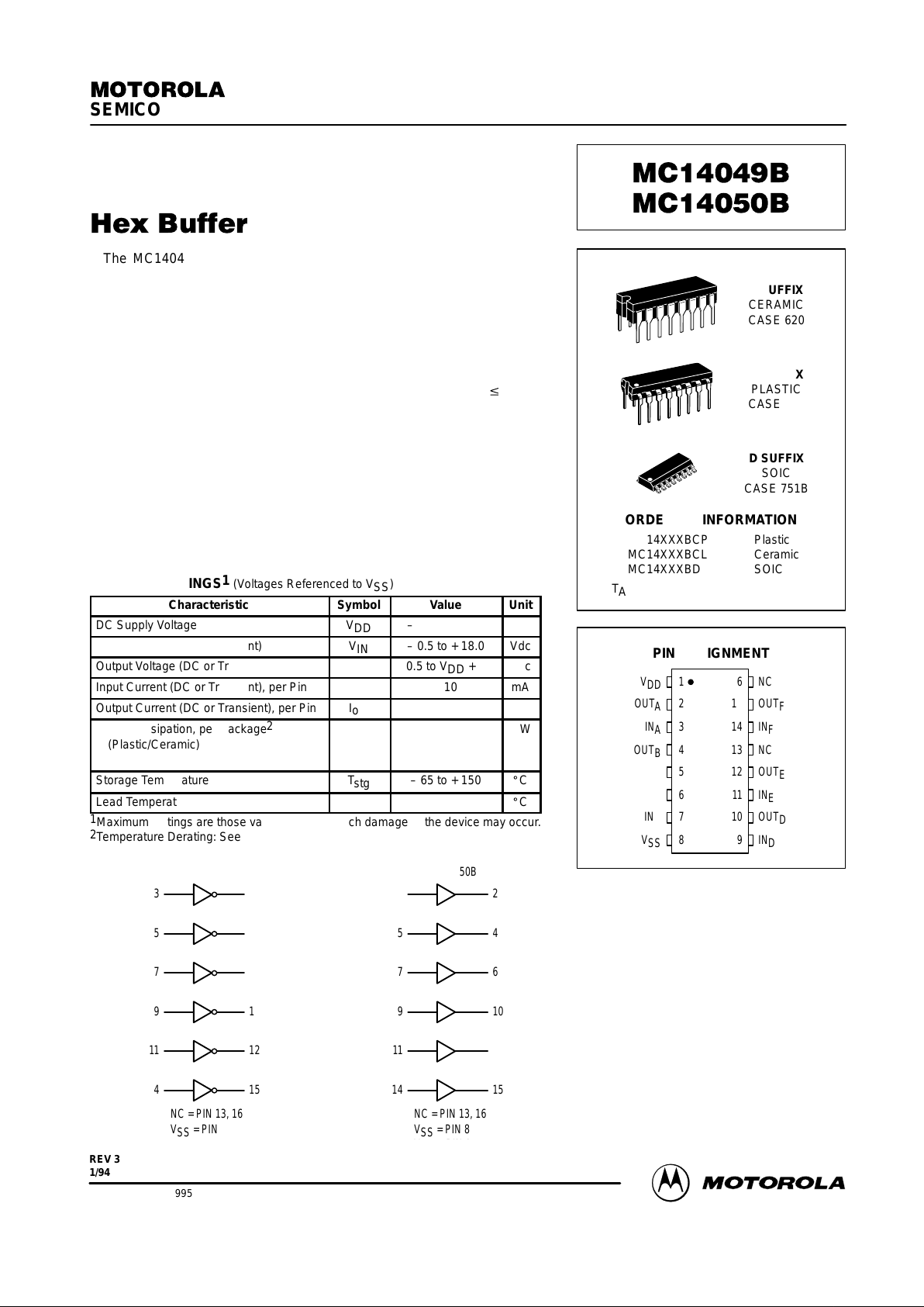
Note that pins 13 and 16 are not connected internally on these devices;
consequently connections to these terminals will not affect circuit operation.
• High Source and Sink Currents
• High–to–Low Level Converter
• Supply Voltage Range = 3.0 V to 18 V
• VIN can exceed V
DD
• Meets JEDEC B Specifications
• Improved ESD Protection On All Inputs
MAXIMUM RATINGS1 (Voltages Referenced to V
SS
)
Characteristic
Symbol
Value
Unit
DC Supply Voltage
V
DD
– 0.5 to + 18.0
Vdc
Input Voltage (DC or Transient)
V
IN
– 0.5 to + 18.0
Vdc
Output Voltage (DC or Transient)
V
out
– 0.5 to VDD + 0.5
Vdc
Input Current (DC or Transient), per Pin
I
in
± 10
mA
Output Current (DC or Transient), per Pin
I
out
+ 45
mA
Power Dissipation, per Package
2
(Plastic/Ceramic)
(SOIC)
P
D
825
740
mW
Storage Temperature
T
stg
– 65 to + 150
_
C
Lead Temperature (8 – Second Soldering)
T
L
260
_
C
1
Maximum Ratings are those values beyond which damage to the device may occur.
2
Temperature Derating: See Figure 3.
LOGIC DIAGRAM
MC14049B
14 15
11
9
7
5
3
12
10
6
4
2
NC = PIN 13, 16
VSS = PIN 8
VDD = PIN 1
MC14050B
14 15
11
9
7
5
3
12
10
6
4
2
NC = PIN 13, 16
VSS = PIN 8
VDD = PIN 1
SEMICONDUCTOR TECHNICAL DATA
Motorola, Inc. 1995
REV 3
1/94
L SUFFIX
CERAMIC
CASE 620
ORDERING INFORMATION
MC14XXXBCP Plastic
MC14XXXBCL Ceramic
MC14XXXBD SOIC
TA = – 55° to 125°C for all packages.
P SUFFIX
PLASTIC
CASE 648
D SUFFIX
SOIC
CASE 751B
PIN ASSIGNMENT
13
14
15
16
9
10
11
125
4
3
2
1
8
7
6
OUT
E
NC
IN
F
OUT
F
NC
IN
D
OUT
D
IN
E
OUT
B
IN
A
OUT
A
V
DD
V
SS
IN
C
OUT
C
IN
B
MOTOROLA CMOS LOGIC DATAMC14049B MC14050B
2
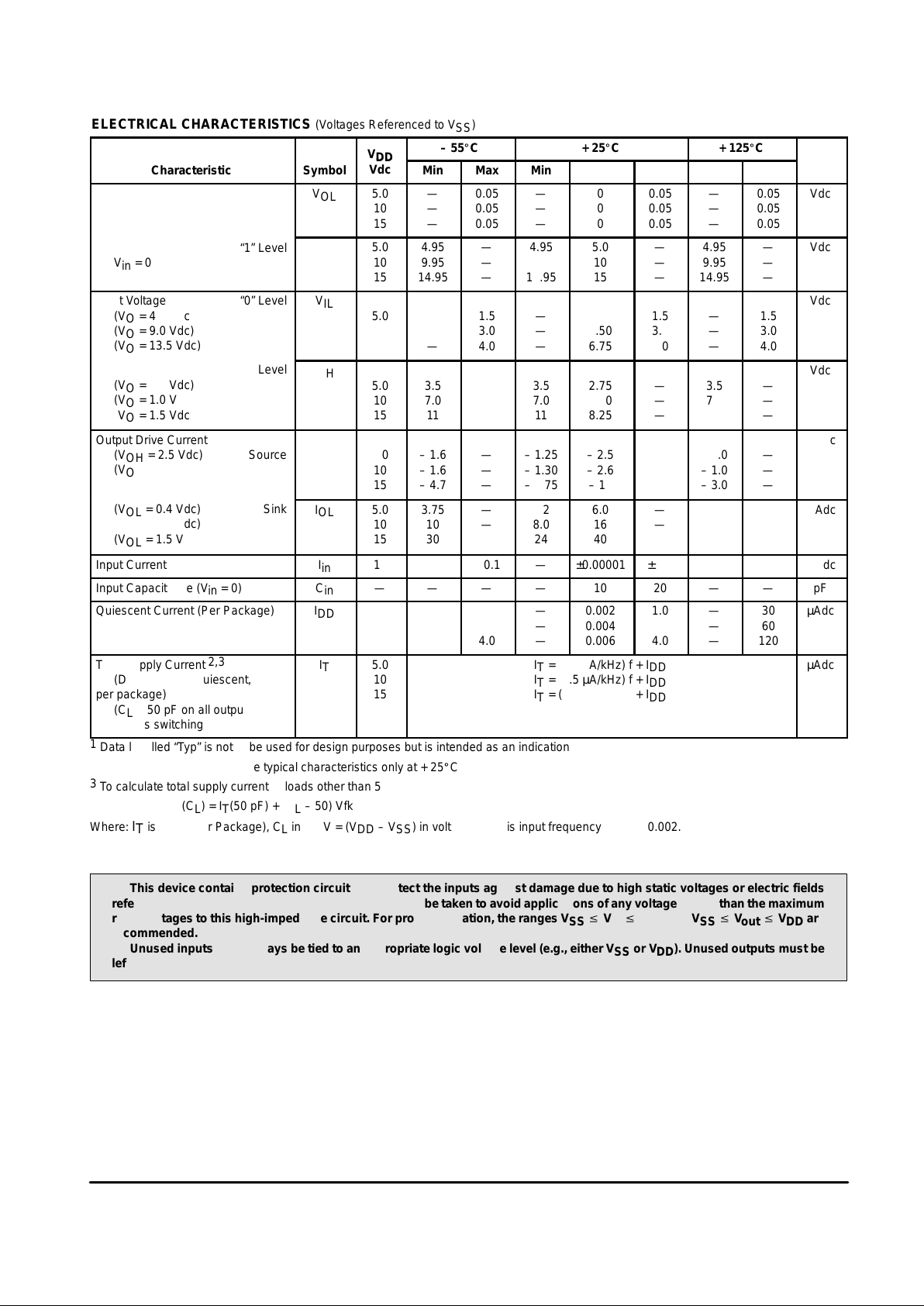
ELECTRICAL CHARACTERISTICS (Voltages Referenced to V
SS
)
V
– 55_C
+ 25_C
+ 125_C
Characteristic
Symbol
V
DD
Vdc
Min
Max
Min
Typ
1
Max
Min
ÎÎÎ
ÎÎÎ
ÎÎÎ
Max
Unit
Output Voltage
“0” Level
Vin = V
DD
V
OL
5.0
10
15
—
—
—
0.05
0.05
0.05
—
—
—
0
0
0
0.05
0.05
0.05
—
—
—
ÎÎÎ
ÎÎÎ
ÎÎÎ
ÎÎÎ
0.05
0.05
0.05
Vdc
“1” Level
Vin = 0
V
OH
5.0
10
15
4.95
9.95
14.95
—
—
—
4.95
9.95
14.95
5.0
10
15
—
—
—
4.95
9.95
14.95
ÎÎÎ
ÎÎÎ
ÎÎÎ
ÎÎÎ
ÎÎÎ
—
—
—
Vdc
Input Voltage
“0” Level
(VO = 4.5 Vdc)
(VO = 9.0 Vdc)
(VO = 13.5 Vdc)
V
IL
5.0
10
15
—
—
—
1.5
3.0
4.0
—
—
—
2.25
4.50
6.75
1.5
3.0
4.0
—
—
—
ÎÎÎ
ÎÎÎ
ÎÎÎ
ÎÎÎ
ÎÎÎ
1.5
3.0
4.0
Vdc
“1” Level
(VO = 0.5 Vdc)
(VO = 1.0 Vdc)
(VO = 1.5 Vdc)
V
IH
5.0
10
15
3.5
7.0
11
—
—
—
3.5
7.0
11
2.75
5.50
8.25
—
—
—
3.5
7.0
11
ÎÎÎ
ÎÎÎ
ÎÎÎ
ÎÎÎ
ÎÎÎ
—
—
—
Vdc
Output Drive Current
(VOH = 2.5 Vdc) Source
(VOH = 9.5 Vdc)
(VOH = 13.5 Vdc)
I
OH
5.0
10
15
– 1.6
– 1.6
– 4.7
—
—
—
– 1.25
– 1.30
– 3.75
– 2.5
– 2.6
– 10
—
—
—
– 1.0
– 1.0
– 3.0
ÎÎÎ
ÎÎÎ
ÎÎÎ
ÎÎÎ
ÎÎÎ
—
—
—
mAdc
(VOL = 0.4 Vdc) Sink
(VOL = 0.5 Vdc)
(VOL = 1.5 Vdc)
I
OL
5.0
10
15
3.75
10
30
—
—
—
3.2
8.0
24
6.0
16
40
—
—
2.6
6.6
19
ÎÎÎ
ÎÎÎ
ÎÎÎ
ÎÎÎ
—
—
—
mAdc
Input Current
I
in
15
—
± 0.1
—
±0.00001
± 0.1
—
ÎÎÎ
ÎÎÎ
ÎÎÎ
± 1.0
µAdc
Input Capacitance (Vin = 0)
C
in
—
—
—
—
10
20
—
ÎÎÎ
ÎÎÎ
ÎÎÎ
—
pF
Quiescent Current (Per Package)
I
DD
5.0
10
15
—
—
—
1.0
2.0
4.0
—
—
—
0.002
0.004
0.006
1.0
2.0
4.0
—
—
—
ÎÎÎ
ÎÎÎ
ÎÎÎ
ÎÎÎ
30
60
120
µAdc
Total Supply Current
2,3
(Dynamic plus Quiescent,
per package)
(CL = 50 pF on all outputs, all
buffers switching
I
T
5.0
10
15
IT = (1.8 µA/kHz) f + I
DD
IT = (3.5 µA/kHz) f + I
DD
IT = (5.3 µA/kHz) f + I
DD
µAdc
1
Data labelled “Typ” is not to be used for design purposes but is intended as an indication of the IC’s potential performance.
2
The formulas given are for the typical characteristics only at + 25_C
3
To calculate total supply current at loads other than 50 pF:
IT(CL) = IT(50 pF) + (CL – 50) Vfk
Where:
I
T
is in µA (per Package), CL in pF, V = (VDD – VSS) in volts, f in kHz is input frequency and k = 0.002.
This device contains protection circuitry to protect the inputs against damage due to high static voltages or electric fields
referenced to the VSS pin only. Extra precautions must be taken to avoid applications of any voltage higher than the maximum
rated voltages to this high-impedance circuit. For proper operation, the ranges VSS v Vin v 18 V and VSS v V
out
v VDD are
recommended.
Unused inputs must always be tied to an appropriate logic voltage level (e.g., either VSS or VDD). Unused outputs must be
left open.
 Loading...