MOTOROLA MC14049BCP, MC14049BD, MC14049BF, MC14049BFL1 Datasheet

Semiconductor Components Industries, LLC, 1999
December, 1999 – Rev. 2
1 Publication Order Number:
1.5SMC6.8A T3/D
1.5SMCXXXAT3 Series
Zener Transient
V oltage Suppressors
GENERAL DATA IS APPLICABLE TO ALL
SERIES IN THIS GROUP
The SMC series is designed to protect voltage sensitive
components from high voltage, high energy transients. They have
excellent clamping capability, high surge capability, low zener
impedance and fast response time. The SMC series is supplied in
ON Semiconductor’s exclusive, cost-effective, highly reliable
Surmetic package and is ideally suited for use in communication
systems, numerical controls, process controls, medical equipment,
business machines, power supplies and many other
industrial/consumer applications.
Specification Features:
• Standard Zener Breakdown Voltage Range — 6.8 to 91 V
• Stand–off Voltage Range — 5.8 to 78 V
• Peak Power — 1500 Watts @ 1 ms
• Maximum Clamp Voltage @ Peak Pulse Current
• Low Leakage < 5 µA Above 10 V
• UL Recognition
• Maximum Temperature Coefficient Specified
• Available in Tape and Reel
• Response Time is Typically < 1 ns
Mechanical Characteristics:
CASE:
Void-free, transfer-molded, thermosetting plastic
FINISH: All external surfaces are corrosion resistant and leads are
readily solderable
POLARITY: Cathode indicated by molded polarity notch. When
operated in zener mode, will be positive with respect to anode
MOUNTING POSITION: Any
LEADS: Modified L–Bend providing more contact area to bond pads
MAXIMUM CASE TEMPERATURE FOR SOLDERING PURPOSES:
260°C for 10 Seconds
WAFER FAB LOCATION: Phoenix, Arizona
ASSEMBLY/TEST LOCATION: Seremban, Malaysia
MAXIMUM RATINGS
Rating Symbol Value Unit
Peak Power Dissipation (1)
@ TL ≤ 25°C
P
PK
1500 Watts
Forward Surge Current (2)
@ TA = 25°C
I
FSM
200 Amps
Thermal Resistance from Junction to Lead (typical)
R
q
JL
15 °C/W
Operating and Storage Temperature Range TJ, T
stg
– 55 to +150 °C
NOTES: 1. Nonrepetitive current pulse per Figure 2 and derated above TA = 25°C per Figure 3.
NOTES: 2. 1/2 sine wave (or equivalent square wave), PW = 8.3 ms, duty cycle = 4 pulses per minute maximum.
PLASTIC SURFACE MOUNT
ZENER OVERVOLTAGE
TRANSIENT SUPPRESSORS
5.8–78 VOLTS
1500 WATT PEAK POWER
Devices listed in
bold, italic
are ON Semiconductor
Preferred devices. Preferred devices are recommended
choices for future use and best overall value.
Device Package Shipping
ORDERING INFORMATION
1.5SMCXXXA T3 SMC Tape and Reel
2500 Units/Reel
SMC
PLASTIC
CASE 403
http://onsemi.com

1.5SMCXXXAT3 Series
http://onsemi.com
2
ELECTRICAL CHARACTERISTICS (T
A
= 25°C unless otherwise noted) VF = 3.5 V Max, IF** = 100 A for all types.
Breakdown Voltage*
Working
Peak
Maximum
Reverse
Maximum
Reverse
Maximum
Reverse Voltage
Maximum
VBR @ I
T
Volts
Reverse
Voltage
Leakage
@ V
RWM
Surge
Current
@ I
RSM
(Clamping Voltage)
Temperature
Coefficient
Device
{{
Min Nom Max mA
V
RWM
Volts
I
R
µA
I
RSM
{
Amps
V
RSM
Volts
of V
BR
%/°C
Device
Marking
1.5SMC6.8AT3
1.5SMC7.5AT3
1.5SMC8.2AT3
1.5SMC9.1AT3
6.45
7.13
7.79
8.65
6.8
7.5
8.2
9.1
7.14
7.88
8.61
9.55
10
10
10
1
5.8
6.4
7.02
7.78
1000
500
200
50
143
132
124
112
10.5
11.3
12.1
13.4
0.057
0.061
0.065
0.068
6V8A
7V5A
8V2A
9V1A
1.5SMC10AT3
1.5SMC11AT3
1.5SMC12AT3
1.5SMC13AT3
9.5
10.5
11.4
12.4
10
11
12
13
10.5
11.6
12.6
13.7
1
1
1
1
8.55
9.4
10.2
11.1
10
5
5
5
103
96
90
82
14.5
15.6
16.7
18.2
0.073
0.075
0.078
0.081
10A
11A
12A
13A
1.5SMC15AT3
1.5SMC16AT3
1.5SMC18AT3
1.5SMC20AT3
14.3
15.2
17.1
19
15
16
18
20
15.8
16.8
18.9
21
1
1
1
1
12.8
13.6
15.3
17.1
5
5
5
5
71
67
59.5
54
21.2
22.5
25.2
27.7
0.084
0.086
0.088
0.09
15A
16A
18A
20A
1.5SMC22AT3
1.5SMC24AT3
1.5SMC27AT3
1.5SMC30AT3
20.9
22.8
25.7
28.5
22
24
27
30
23.1
25.2
28.4
31.5
1
1
1
1
18.8
20.5
23.1
25.6
5
5
5
5
49
45
40
36
30.6
33.2
37.5
41.4
0.092
0.094
0.096
0.097
22A
24A
27A
30A
1.5SMC33AT3
1.5SMC36AT3
1.5SMC39AT3
1.5SMC43AT3
31.4
34.2
37.1
40.9
33
36
39
43
34.7
37.8
41
45.2
1
1
1
1
28.2
30.8
33.3
36.8
5
5
5
5
33
30
28
25.3
45.7
49.9
53.9
59.3
0.098
0.099
0.1
0.101
33A
36A
39A
43A
1.5SMC47AT3
1.5SMC51AT3
1.5SMC56AT3
1.5SMC62AT3
44.7
48.5
53.2
58.9
47
51
56
62
49.4
53.6
58.8
65.1
1
1
1
1
40.2
43.6
47.8
53
5
5
5
5
23.2
21.4
19.5
17.7
64.8
70.1
77
85
0.101
0.102
0.103
0.104
47A
51A
56A
62A
1.5SMC68AT3
1.5SMC75AT3
1.5SMC82AT3
1.5SMC91AT3
64.6
71.3
77.9
86.5
68
75
82
91
71.4
78.8
86.1
95.5
1
1
1
1
58.1
64.1
70.1
77.8
5
5
5
5
16.3
14.6
13.3
12
92
103
113
125
0.104
0.105
0.105
0.106
68A
75A
82A
91A
Devices listed in bold, italic are ON Semiconductor Preferred devices.
* * VBR measured at pulse test current IT at an ambient temperaure of 25°C.
* * 1/2 sine wave (or equivalent square wave), PW = 8.3 ms, duty cycle = 4 pulses per minute maximum.
{{
Surge current waveform per Figure 2 and derate per Figure 3 of General Data — 1500 Watt at the beginning of this group.
{{
T3 suffix designates tape and reel of 2500 units.

1.5SMCXXXAT3 Series
http://onsemi.com
3
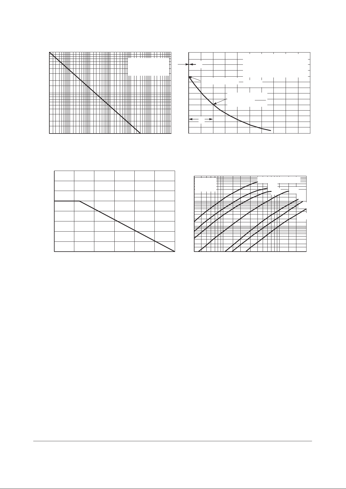
P , PEAK POWER (kW)
P
NONREPETITIVE
PULSE WAVEFORM
SHOWN IN FIGURE 2
tP, PULSE WIDTH
1
10
100
0.1
µs1 µs10 µs 100 µs
1 ms 10 ms
Figure 1. Pulse Rating Curve
01234
0
50
100
t, TIME (ms)
VALUE (%)
HALF VALUE –
I
RSM
2
PEAK VALUE – I
RSM
t
r
tr≤ 10 µs
Figure 2. Pulse Waveform
Figure 3. Pulse Derating Curve
PEAK PULSE DERATING IN % OF
PEAK POWER OR CURRENT @ T
A
= 25 C°
100
80
60
40
20
0
0 25 50 75 100 125 150
TA, AMBIENT TEMPERATURE (°C)
120
140
160
t
P
PULSE WIDTH (tP) IS DEFINED
AS THAT POINT WHERE THE PEAK
CURRENT DECAYS TO 50%
OF I
RSM
.
∆VZ, INSTANTANEOUS INCREASE IN VZ ABOVE VZ (NOM) (VOLTS)
0.3 0.5 0.7 1 2 3 5 7 10 20 30
I
Z
, ZENER CURRENT (AMPS)
1000
500
200
100
50
1
2
5
10
20
TL=25°C
tP=10µs
VZ(NOM) = 6.8 TO 13 V
20 V
24 V
43 V
75 V
120 V
180 V
Figure 4. Dynamic Impedance
UL RECOGNITION
The entire series has Underwriters Laboratory
Recognition for the classification of protectors (QVGV2)
under the UL standard for safety 497B and File #116110.
Many competitors only have one or two devices recognized
or have recognition in a non-protective category. Some
competitors have no recognition at all. With the UL497B
recognition, our parts successfully passed several tests
including Strike Voltage Breakdown test, Endurance
Conditioning, Temperature test, Dielectric
Voltage-Withstand test, Discharge test and several more.
Whereas, some competitors have only passed a
flammability test for the package material, we have been
recognized for much more to be included in their Protector
category .
 Loading...