

Motorola MC14046BCL, MC14046BDW, MC14046BCP Datasheet
MOTOROLA CMOS LOGIC DATA
1
MC14046B
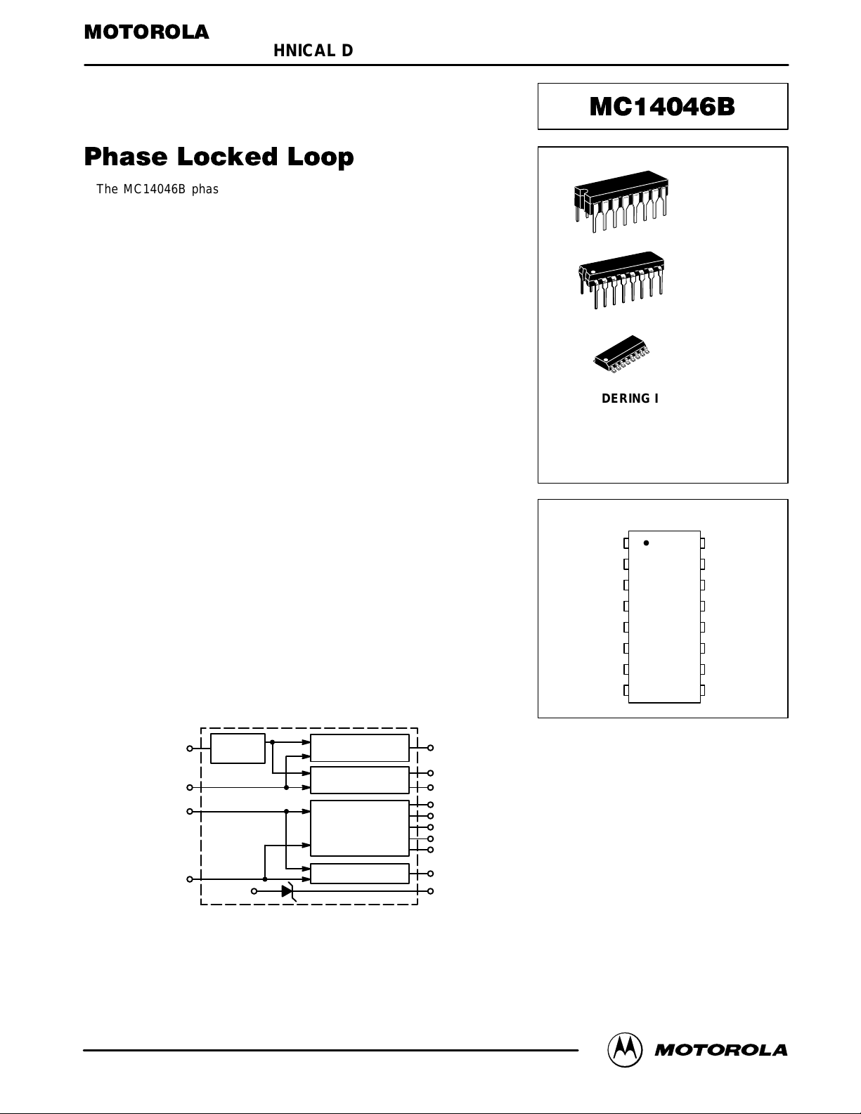
The MC14046B phase locked loop contains two phase comparators, a
voltage–controlled oscillator (VCO), source follower, and zener diode. The
comparators have two common signal inputs, PCAin and PCBin. Input PCA
in
can be used directly coupled to large voltage signals, or indirectly coupled
(with a series capacitor) to small voltage signals. The self–bias circuit
adjusts small voltage signals in the linear region of the amplifier. Phase
comparator 1 (an exclusive OR gate) provides a digital error signal PC1
out
,
and maintains 90° phase shift at the center frequency between PCAin and
PCBin signals (both at 50% duty cycle). Phase comparator 2 (with leading
edge sensing logic) provides digital error signals, PC2
out
and LD, and
maintains a 0° phase shift between PCAin and PCBin signals (duty cycle is
immaterial). The linear VCO produces an output signal VCO
out
whose
frequency is determined by the voltage of input VCOin and the capacitor and
resistors connected to pins C1A, C1B, R1, and R2. The source–follower
output SF
out
with an external resistor is used where the VCOin signal is
needed but no loading can be tolerated. The inhibit input Inh, when high,
disables t he VCO a nd s ource follower t o minimize s tandby p ower
consumption. The zener diode can be used to a ssist in p ower supply
regulation.
Applications include FM and F SK modulation and d emodulation, frequency synthesis and multiplication, frequency discrimination, tone decoding, d ata synchronization a nd conditioning, voltage–to–frequency
conversion and motor speed control.
• Buffered Outputs Compatible with MHTL and Low–Power TTL
• Diode Protection on All Inputs
• Supply Voltage Range = 3.0 to 18 V
• Pin–for–Pin Replacement for CD4046B
• Phase Comparator 1 is an Exclusive Or Gate and is Duty Cycle Limited
• Phase Comparator 2 switches on Rising Edges and is not Duty Cycle
Limited
BLOCK DIAGRAM
PCA
in
PCB
in
VCO
in
INH
14
3
9
5
VDD = PIN 16
VSS = PIN 8
2 PC1
out
13 PC2
out
1 LD
4 VCO
out
11 R1
12 R2
6 C1
A
7 C1
B
10 SF
out
15 ZENERV
SS
SELF BIAS
CIRCUIT
PHASE
COMPARATOR 1
PHASE
COMPARATOR 2
VOLTAGE
CONTROLLED
OSCILLATOR
(VCO)
SOURCE FOLLOWER
SEMICONDUCTOR TECHNICAL DATA
Motorola, Inc. 1995
REV 3
1/94
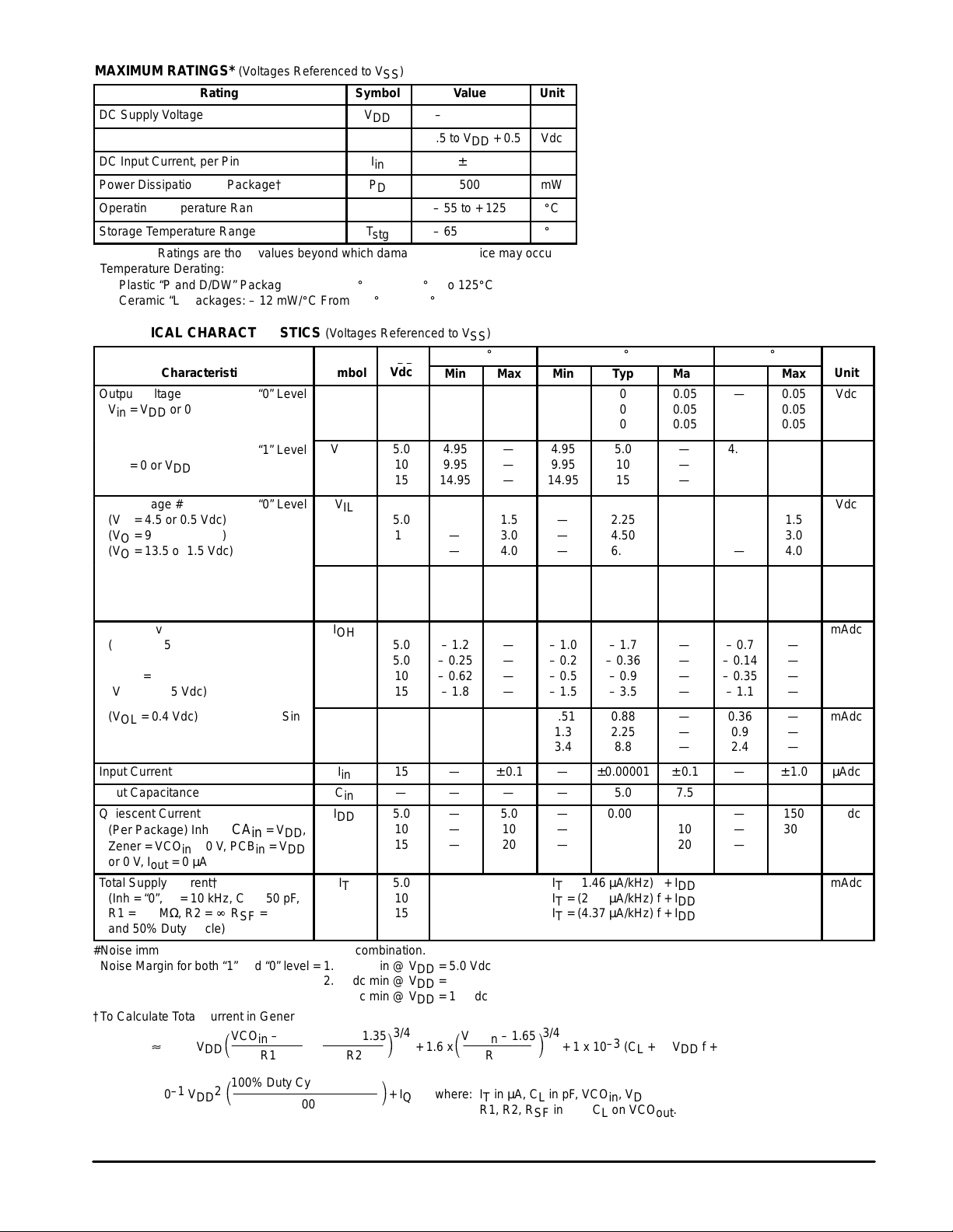
L SUFFIX
CERAMIC
CASE 620
ORDERING INFORMATION
MC14XXXBCP Plastic
MC14XXXBCL Ceramic
MC14XXXBDW SOIC
TA = – 55° to 125°C for all packages.
P SUFFIX
PLASTIC
CASE 648
DW SUFFIX
SOIC
CASE 751G
PIN ASSIGNMENT
13
14
15
16
9
10
11
125
4
3
2
1
8
7
6
R2
PC2
out
PCA
in
ZENER
V
DD
VCO
in
SF
out
R1
VCO
out
PCB
in
PC1
out
LD
V
SS
C1
B
C1
A
INH
MOTOROLA CMOS LOGIC DATAMC14046B
2
MAXIMUM RATINGS* (Voltages Referenced to V
SS
)
Rating
Symbol
Value
Unit
DC Supply Voltage
V
DD
– 0.5 to + 18
Vdc
Input Voltage, All Inputs
V
in
– 0.5 to VDD + 0.5
Vdc
DC Input Current, per Pin
I
in
± 10
mAdc
Power Dissipation, per Package†
P
D
500
mW
Operating Temperature Range
T
A
– 55 to + 125
_
C
Storage Temperature Range
T
stg
– 65 to + 150
_
C
*Maximum Ratings are those values beyond which damage to the device may occur.
†Temperature Derating:
Plastic “P and D/DW” Packages: – 7.0 mW/_C From 65_C To 125_C
Ceramic “L” Packages: – 12 mW/_C From 100_C To 125_C
ELECTRICAL CHARACTERISTICS (Voltages Referenced to V
SS
)
V
DD
– 55_C
25_C
125_C
Characteristic
Symbol
V
DD
Vdc
Min
Max
Min
Typ
Max
Min
Max
Unit
“0” Level
Vin = VDD or 0
V
OL
5.0
10
15
—
—
—
0.05
0.05
0.05
—
—
—
0
0
0
0.05
0.05
0.05
—
—
—
0.05
0.05
0.05
Vdc
“1” Level
Vin = 0 or V
DD
V
OH
5.0
10
15
4.95
9.95
14.95
—
—
—
4.95
9.95
14.95
5.0
10
15
—
—
—
4.95
9.95
14.95
—
—
—
Vdc
“0” Level
(VO = 4.5 or 0.5 Vdc)
(VO = 9.0 or 1.0 Vdc)
(VO = 13.5 or 1.5 Vdc)
V
IL
5.0
10
15
—
—
—
1.5
3.0
4.0
—
—
—
2.25
4.50
6.75
1.5
3.0
4.0
—
—
—
1.5
3.0
4.0
Vdc
“1” Level
(VO = 1.0 or 9.0 Vdc)
(VO = 1.5 or 13.5 Vdc)
V
IH
5.0
10
15
3.5
7.0
11
—
—
—
3.5
7.0
11
2.75
5.50
8.25
—
—
—
3.5
7.0
11
—
—
—
Vdc
I
OH
5.0
5.0
10
15
– 1.2
– 0.25
– 0.62
– 1.8
—
—
—
—
– 1.0
– 0.2
– 0.5
– 1.5
– 1.7
– 0.36
– 0.9
– 3.5
—
—
—
—
– 0.7
– 0.14
– 0.35
– 1.1
—
—
—
—
mAdc
I
OL
5.0
10
15
0.64
1.6
4.2
—
—
—
0.51
1.3
3.4
0.88
2.25
8.8
—
—
—
0.36
0.9
2.4
—
—
—
mAdc
Input Current
I
in
15
—
± 0.1
—
±0.00001
± 0.1
—
± 1.0
µAdc
Input Capacitance
C
in
—
—
—
—
5.0
7.5
—
—
pF
Quiescent Current
(Per Package) Inh =
PCA
in
= VDD,
Zener = VCOin = 0 V, PCBin = V
DD
or 0 V, I
out
= 0 µA
I
DD
5.0
10
15
—
—
—
5.0
10
20
—
—
—
0.005
0.010
0.015
5.0
10
20
—
—
—
150
300
600
µAdc
Total Supply Current†
(Inh = “0”, fo = 10 kHz, CL = 50 pF,
R1 = 1.0 MΩ, R2 = R RSF = ∞,
and 50% Duty Cycle)
I
T
5.0
10
15
IT = (1.46 µA/kHz) f + I
DD
IT = (2.91 µA/kHz) f + I
DD
IT = (4.37 µA/kHz) f + I
DD
mAdc
#Noise immunity specified for worst–case input combination.
Noise Margin for both “1” and “0” level = 1.0 Vdc min @ VDD = 5.0 Vdc
2.0 Vdc min @ VDD = 10 Vdc
2.5 Vdc min @ VDD = 15 Vdc
†To Calculate Total Current in General:
IT [ 2.2 x V
DD
+ 1 x 10⁻³ (CL + 9) VDD f +
VCOin – 1.65
Ǔǒ
+
VDD – 1.35
3/4
R1 R2
VCOin – 1.65
3/4
+ 1.6 x
where: IT in µA, CL in pF, VCOin, VDD in Vdc, f in kHz, and
R1, R2, RSF in MΩ, CL on VCO
out
.
ǒ Ǔ
R
SF
1 x 10⁻¹ V
DD
2
100% Duty Cycle of PCA
in
100
+ I
Q
Ǔǒ
Output Voltage
Input Voltage #
(VO = 0.5 or 4.5 Vdc)
Output Drive Current
(VOH = 2.5 Vdc) Source
(VOH = 4.6 Vdc)
(VOH = 9.5 Vdc)
(VOH = 13.5 Vdc)
(VOL = 0.4 Vdc) Sink
(VOL = 0.5 Vdc)
(VOL = 1.5 Vdc)
MOTOROLA CMOS LOGIC DATA
3
MC14046B
ELECTRICAL CHARACTERISTICS* (C
L
= 50 pF, TA = 25°C)
Minimum
Maximum
Characteristic
Symbol
V
DD
Vdc
Device
Typical
Device
Units
Output Rise Time
t
TLH
= (3.0 ns/pF) CL + 30 ns
t
TLH
= (1.5 ns/pF) CL + 15 ns
t
TLH
= (1.1 ns/pF) CL + 10 ns
t
TLH
5.0
10
15
—
—
—
180
90
65
350
150
110
ns
Output Fall Time
t
THL
= (1.5 ns/pF) CL + 25 ns
t
THL
= (0.75 ns/pF) CL + 12.5 ns
t
THL
= (0.55 ns/pF) CL + 9.5 ns
t
THL
5.0
10
15
—
—
—
100
50
37
175
75
55
ns
PHASE COMPARATORS 1 and 2
R
in
5.0
10
15
1.0
0.2
0.1
2.0
0.4
0.2
—
—
—
MΩ
R
in
15
150
1500
—
MΩ
Minimum Input Sensitivity
AC Coupled — PCA
in
C series = 1000 pF, f = 50 kHz
V
in
5.0
10
15
—
—
—
200
400
700
300
600
1050
mV p–p
DC Coupled — PCAin, PCB
in
—
5 to 15
See Noise Immunity
VOLTAGE CONTROLLED OSCILLATOR (VCO)
Maximum Frequency
(VCOin = VDD, C1 = 50 pF
R1 = 5.0 kΩ, and R2 = ∞)
f
max
5.0
10
15
0.5
1.0
1.4
0.7
1.4
1.9
—
—
—
MHz
Temperature — Frequency Stability
(R2 = ∞ )
—
5.0
10
15
—
—
—
0.12
0.04
0.015
—
—
—
%/_C
Linearity (R2 = ∞ )
(VCOin = 2.5 V ± 0.3 V, R1 > 10 kΩ)
(VCOin = 5.0 V ± 2.5 V, R1 > 400 kΩ)
(VCOin = 7.5 V ± 5.0 V, R1 ≥ 1000 kΩ)
—
5.0
10
15
—
—
—
1.0
1.0
1.0
—
—
—
%
Output Duty Cycle
—
5 to 15
—
50
—
%
Input Resistance — VCO
in
R
in
15
150
1500
—
MΩ
SOURCE–FOLLOWER
Offset Voltage
(VCOin minus SF
out
, RSF > 500 kΩ)
—
5.0
10
15
—
—
—
1.65
1.65
1.65
2.2
2.2
2.2
V
Linearity
(VCOin = 2.5 V ± 0.3 V, RSF > 50 kΩ)
(VCOin = 5.0 V ± 2.5 V, RSF > 50 kΩ)
(VCOin = 7.5 V ± 5.0 V, RSF > 50 kΩ)
—
5.0
10
15
—
—
—
0.1
0.6
0.8
—
—
—
%
ZENER DIODE
Zener Voltage (Iz = 50 µA)
V
Z
—
6.7
7.0
7.3
V
Dynamic Resistance (Iz = 1.0 mA)
R
Z
—
—
100
—
Ω
*The formula given is for the typical characteristics only.
Input Resistance — PCA
— PCB
in
in
 Loading...