

Motorola MC14000UBCL, MC14000UBCP, MC14000UBD Datasheet
MOTOROLA CMOS LOGIC DATAMC14000UB
2
The MC14000UB dual 3–input NOR gate plus inverter is constructed with
MOS P–channel and N–channel enhancement mode devices in a single
monolithic structure. These complementary MOS logic gates find primary
use where low power dissipation and/or high noise immunity is desired.
• Diode Protection on All Inputs
• Supply Voltage Range = 3.0 Vdc to 18 Vdc
• Logic Swing Independent of Fanout
• Pin–for–Pin Replacement for CD4000UB
MAXIMUM RATINGS* (Voltages Referenced to V
SS
)
Symbol
Parameter
Value
Unit
V
DD
DC Supply Voltage
– 0.5 to + 18.0
V
Vin, V
out
Input or Output Voltage (DC or Transient)
– 0.5 to VDD + 0.5
V
lin, l
out
Input or Output Current (DC or Transient),
per Pin
± 10
mA
P
D
Power Dissipation, per Package†
500
mW
T
stg
Storage Temperature
– 65 to + 150
_
C
T
L
Lead Temperature (8–Second Soldering)
260
_
C
*Maximum Ratings are those values beyond which damage to the device may occur.
†Temperature Derating:
Plastic “P and D/DW” Packages: – 7.0 mW/_C From 65_C To 125_C
Ceramic “L” Packages: – 12 mW/_C From 100_C To 125_C
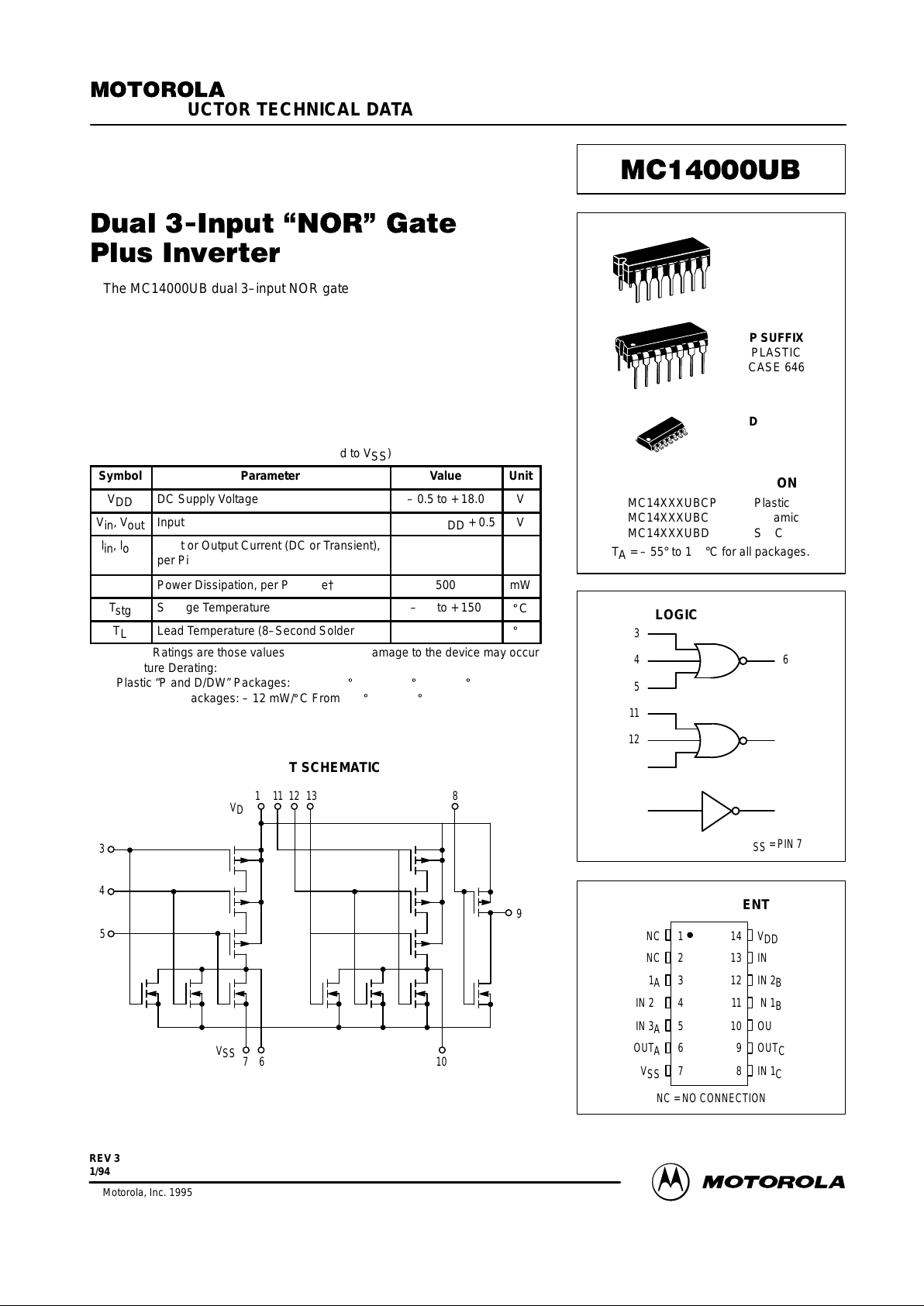
CIRCUIT SCHEMATIC
14 11 12 13 8
67 10
V
SS
9
3
4
5
V
DD
SEMICONDUCTOR TECHNICAL DATA
Motorola, Inc. 1995
REV 3
1/94
LOGIC DIAGRAM
L SUFFIX
CERAMIC
CASE 632
ORDERING INFORMATION
MC14XXXUBCP Plastic
MC14XXXUBCL Ceramic
MC14XXXUBD SOIC
TA = – 55° to 125°C for all packages.
P SUFFIX
PLASTIC
CASE 646
D SUFFIX
SOIC
CASE 751A
PIN ASSIGNMENT
11
12
13
14
8
9
105
4
3
2
1
7
6
OUT
B
IN 1
B
IN 2
B
IN 3
B
V
DD
IN 1
C
OUT
C
IN 2
A
IN 1
A
NC
NC
V
SS
OUT
A
IN 3
A
NC = NO CONNECTION
3
4
5
6
11
12
13
10
8 9
VDD = PIN 14
VSS = PIN 7
MOTOROLA CMOS LOGIC DATA
3
MC14000UB
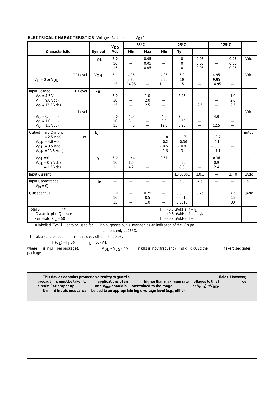
ELECTRICAL CHARACTERISTICS (Voltages Referenced to V
SS
)
V
– 55_C
25_C
+ 125_C
Characteristic
Symbol
V
DD
Vdc
Min
Max
Min
Typ #
Max
Min
ÎÎÎ
ÎÎÎ
ÎÎÎ
Max
Unit
Output Voltage “0” Level
Vin = VDD or 0
V
OL
5.0
10
15
—
—
—
0.05
0.05
0.05
—
—
—
0
0
0
0.05
0.05
0.05
—
—
—
ÎÎÎ
ÎÎÎ
ÎÎÎ
ÎÎÎ
0.05
0.05
0.05
Vdc
“1” Level
Vin = 0 or V
DD
V
OH
5.0
10
15
4.95
9.95
14.95
—
—
—
4.95
9.95
14.95
5.0
10
15
—
—
—
4.95
9.95
14.95
ÎÎÎ
ÎÎÎ
ÎÎÎ
ÎÎÎ
ÎÎÎ
—
—
—
Vdc
Input Voltage “0” Level
(VO = 4.5 Vdc)
(VO = 9.0 Vdc)
(VO = 13.5 Vdc)
V
IL
5.0
10
15
—
—
—
1.0
2.0
2.5
—
—
—
2.25
4.50
6.75
1.0
2.0
2.5
—
—
—
ÎÎÎ
ÎÎÎ
ÎÎÎ
ÎÎÎ
ÎÎÎ
1.0
2.0
2.5
Vdc
“1” Level
(VO = 0.5 Vdc)
(VO = 1.0 Vdc)
(VO = 1.5 Vdc)
V
IH
5.0
10
15
4.0
8.0
12.5
—
—
—
4.0
8.0
12.5
2.75
5.50
8.25
—
—
—
4.0
8.0
12.5
ÎÎÎ
ÎÎÎ
ÎÎÎ
ÎÎÎ
ÎÎÎ
—
—
—
Vdc
Output Drive Current
(VOH = 2.5 Vdc) Source
(VOH = 4.6 Vdc)
(VOH = 9.5 Vdc)
(VOH = 13.5 Vdc)
I
OH
5.0
5.0
10
15
– 1.2
– 0.25
– 0.62
– 1.8
—
—
—
—
– 1.0
– 0.2
– 0.5
– 1.5
– 1.7
– 0.36
– 0.9
– 3.5
—
—
—
—
– 0.7
– 0.14
– 0.35
– 1.1
ÎÎÎ
ÎÎÎ
ÎÎÎ
ÎÎÎ
ÎÎÎ
—
—
—
—
mAdc
(VOL = 0.4 Vdc) Sink
(VOL = 0.5 Vdc)
(VOL = 1.5 Vdc)
I
OL
5.0
10
15
0.64
1.6
4.2
—
—
—
0.51
1.3
3.4
0.88
2.25
8.8
—
—
—
0.36
0.9
2.4
ÎÎÎ
ÎÎÎ
ÎÎÎ
ÎÎÎ
—
—
—
mAdc
Input Current
I
in
15
—
± 0.1
—
±0.00001
± 0.1
—
ÎÎÎ
ÎÎÎ
ÎÎÎ
± 1.0
µAdc
Input Capacitance
(Vin = 0)
C
in
—
—
—
—
5.0
7.5
—
ÎÎÎ
ÎÎÎ
ÎÎÎ
ÎÎÎ
—
pF
Quiescent Current
(Per Package)
I
DD
5.0
10
15
—
—
—
0.25
0.5
1.0
—
—
—
0.0005
0.0010
0.0015
0.25
0.5
1.0
—
—
—
ÎÎÎ
ÎÎÎ
ÎÎÎ
ÎÎÎ
7.5
15
30
µAdc
Total Supply Current**†
(Dynamic plus Quiescent,
Per Gate, CL = 50 pF)
I
T
5.0
10
15
IT = (0.3 µA/kHz) f + IDD/N
IT = (0.6 µA/kHz) f + IDD/N
IT = (0.8 µA/kHz) f + IDD/N
µAdc
#Data labelled “Typ” is not to be used for design purposes but is intended as an indication of the IC’s potential performance.
**The formulas given are for the typical characteristics only at 25_C.
†To calculate total supply current at loads other than 50 pF:
IT(CL) = IT(50 pF) + (CL – 50) Vfk
where: IT is in µH (per package), CL in pF , V = (VDD – VSS) in volts, f in kHz is input frequency, and k = 0.001 x the number of exercised gates per
package.
This device contains protection circuitry to guard against damage due to high static voltages or electric fields. However,
precautions must be taken to avoid applications of any voltage higher than maximum rated voltages to this high-impedance
circuit. For proper operation, Vin and V
out
should be constrained to the range VSS ≤ (Vin or V
out
) ≤ VDD.
Unused inputs must always be tied to an appropriate logic voltage level (e.g., either VSS or VDD). Unused outputs must
be left open.
 Loading...