

Motorola MC1391P Datasheet
Device
Operating
Temperature Range
Package
SEMICONDUCTOR
TECHNICAL DATA
TV HORIZONTAL
PROCESSOR
ORDERING INFORMATION
MC1391P TA = 0° to +70°C Plastic DIP
Order this document by MC1391/D
P SUFFIX
PLASTIC PACKAGE
CASE 626
8
1
1
MOTOROLA ANALOG IC DEVICE DATA
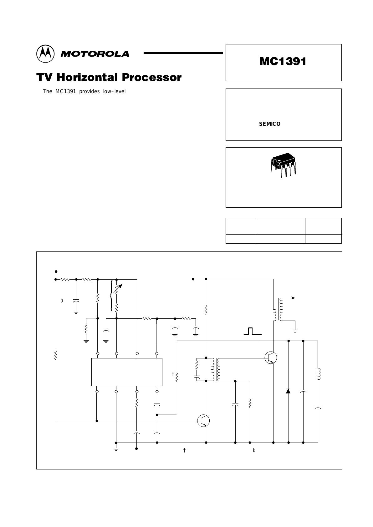
The MC1391 provides low–level horizontal sections including phase
detector, oscillator and pre–driver. This device was designed for use in all
types of television receivers.
• Internal Shunt Regulator
• Preset Hold Control Capability
• ±300 Hz Typical Pull–In
• Linear Balanced Phase Detector
• Variable Output Duty Cycle for Driving Tube or Transistor
• Low Thermal Frequency Drift
• Small Static Phase Error
• Adjustable DC Loop Gain
• Positive Flyback Inputs
Figure 1. Simplified Application
–20V Sync
MC1391P
2.2kR
F
To
High
Voltage
Tripler
Y
O
K
E
MRD
1140
or
Equiv
1.5
5.0
µ
F
MPS–U04
or Equiv
4k
10W
C
C
+
1
µ
F
150k
Ry
R
x
3.3k
C
B
15.3:1
15k
2143
39k
0.1
µ
F
R
Z
{
82k
+150V
3k
Hold
12k
R
C
R
D
2.7k
+
C
A
100
µ
F
R
E
2.4k
5768
MJ105 or Equiv
R
A
R
B
V
nonreg
+ 30V
470 470
0.0068
µ
F
0.005
µ
F
0.01
µ
F
0.2
µ
F
0.1
µ
F
0.003
µ
F
This circuit has an oscillator pull–in range of
±
300 Hz, a noise bandwidth of 320 Hz, and a damping factor of 0.8.
{
RZ = 6.8 k per 100 V of flyback amplitude.
0.001
µ
F
Motorola, Inc. 1996 Rev 2
MC1391
2
MOTOROLA ANALOG IC DEVICE DATA
MAXIMUM RATINGS
(TA = +25°C, unless otherwise noted.)
Rating
Value Unit
Supply Current 40 mAdc
Output Voltage 40 Vdc
Output Current 30 mAdc
Sync Input Voltage (Pin 3) 5.0 V
pp
Flyback Input Voltage (Pin 4) 5.0 V
pp
Power Dissipation (Package Limitation)
Plastic Package
Derate above TA = +25°C
625
5.0
mW
mW/°C
Operating T emperature Range (Ambient) 0 to +70 °C
Storage Temperature Range –65 to +150 °C
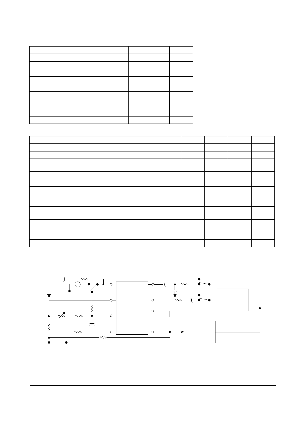
ELECTRICAL CHARACTERISTICS (T
A
= +25°C, unless otherwise noted. See Test Circuit of Figure 2, all switches in position 1.)
Characteristics
Min Typ Max Unit
Regulated Voltage (Pin 6) 8.0 8.6 9.4 Vdc
Supply Current (Pin 6) – 20 – mAdc
Collector–Emitter Saturation Voltage (Output Transistor Q1 in Figure 6)
(IC = 20 mA, Pin 1 ) Vdc
– 0.15 0.25
Vdc
Voltage (Pin 4) – 2.0 – Vdc
Oscillator Pull–in Range (Adjust RH in Figure 2) – ±300 – Hz
Oscillator Hold–in Range (Adjust RH in Figure 2) – ±900 – Hz
Static Phase Error
(∆f = 300 Hz)
– 0.5 –
µs
Free–running Frequency Supply Dependance
(S1 in position 2)
– ±3.0 –
Hz/Vdc
Phase Detector Leakage (Pin 5)
(All switches in position 2)
– – ±1.0
µA
Sync Input Voltage (Pin 3) 2.0 – 5.0 V
pp
Sawtooth Input Voltage (Pin 4) 1.0 – 3.0 V
pp
Figure 2. Test Circuit
MC1391P
Output
Pulse
+30V
1
2
3
4
39k
1
2
2
S2
S3
0.1
µ
F
5
6
7
8
S1
1
150k
3.3k
+
–
2
+4.0V
12k
3.0k
R
H
1.0k
1.0k
2.0k
6800pF
V
M
VCC +30V
Pulse Generator
Output = +50 V
12
µ
s
Pulse Generator
Sync Pulse =
–20 V , 5.0
µ
s,
fO = 15.750 Hz
1
0.1µF
0.003
µ
F
µ
A
(See Figure 5)
0.1
µ
F
+
3.3k
 Loading...